LM2596(开关电压调节器)中文版
- 格式:pdf
- 大小:864.96 KB
- 文档页数:18
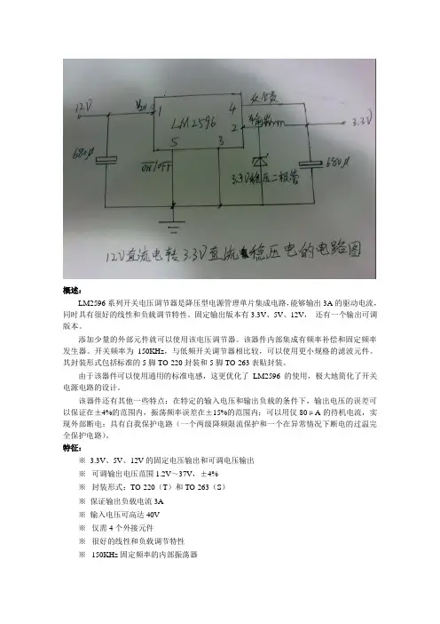
概述:LM2596系列开关电压调节器是降压型电源管理单片集成电路,能够输出3A的驱动电流,同时具有很好的线性和负载调节特性。
固定输出版本有3.3V、5V、12V,还有一个输出可调版本。
添加少量的外部元件就可以使用该电压调节器。
该器件内部集成有频率补偿和固定频率发生器。
开关频率为150KHz,与低频开关调节器相比较,可以使用更小规格的滤波元件。
其封装形式包括标准的5脚TO-220封装和5脚TO-263表贴封装。
由于该器件可以使用通用的标准电感,这更优化了LM2596的使用,极大地简化了开关电源电路的设计。
该器件还有其他一些特点:在特定的输入电压和输出负载的条件下,输出电压的误差可以保证在±4%的范围内,振荡频率误差在±15%的范围内;可以用仅80μA的待机电流,实现外部断电;具有自我保护电路(一个两级降频限流保护和一个在异常情况下断电的过温完全保护电路)。
特征:※ 3.3V、5V、12V的固定电压输出和可调电压输出※可调输出电压范围1.2V~37V,±4%※封装形式:TO-220(T)和TO-263(S)※保证输出负载电流3A※输入电压可高达40V※仅需4个外接元件※很好的线性和负载调节特性※150KHz固定频率的内部振荡器※TTL关断能力※低功耗待机模式,I Q的典型值为80μA※高转换效率※使用容易购买的标准电感※具有过热保护和限流保护功能应用:※简易高效率降压调节器※在卡上的开关电压调节器※正到负电压转换器专利号:5382918典型电路(固定输出电压版本):封装和型号:※弯曲交叉的引脚,通孔封装,5脚TO-220 (T)订货型号:LM2596T-3.3, LM2596T-5.0,LM2596T-12 or LM2596T-ADJ ※表面贴封装,5脚TO-263 (S)订货型号:LM2596S-3.3, LM2596S-5.0, LM2596S-12 or LM2596S-ADJ极限条件:最大供电电压45VON /OFF 管脚输入电压-0.3≤V≤+25V反馈脚电压-0.3≤V≤+25V输出电压到地(稳态)-1V功率消耗内部限定储存温度-65°C 到+150°CESD易感性(人体模式)2KV焊接温度T封装(锡焊, 10秒) +260°C最大结温+150°C运行条件:温度范围-40°C≤T J≤+125°C供电电压 4.5V 到40VLM2596-3.3电参数说明:标准字体对应的项目适合于TJ=25℃时,粗体字对应的项目适合于全温度范围符号意义测试条件典型值(注3)极限值(注4)单位(极限)系统参数(注5) 测试电路图 1V OUT输出电压 4.75V ≤ V IN≤ 40V,0.2A ≤ I LOAD≤ 3A 3.33.168/3.1353.432/3.465VV(min)V(max)η效率V IN = 12V,I LOAD = 3A73 %LM2596-5.0电参数说明:标准字体对应的项目适合于TJ=25℃时,粗体字对应的项目适合于全温度范围符号意义测试条件典型值(注3)极限值(注4)单位(极限)系统参数(注5) 测试电路图 1V OUT输出电压7V ≤ V IN ≤ 40V,0.2A ≤ I LOAD≤ 3A 5.04.800/4.7505.200/5.250VV(min)V(max)η效率V IN = 12V,I LOAD = 3A80 %LM2596-12电参数说明:标准字体对应的项目适合于TJ=25℃时,粗体字对应的项目适合于全温度范围符号意义测试条件典型值(注3)极限值(注4)单位(极限)系统参数(注5) 测试电路图 1V OUT输出电压15V ≤ V IN≤ 40V,0.2A ≤ I LOAD≤ 3A 12.011.52/11.4012.48/12.60VV(min)V(max)η效率V IN = 25V,I LOAD = 3A90 %LM2596-ADJ电参数说明:标准字体对应的项目适合于TJ=25℃时,粗体字对应的项目适合于全温度范围符号意义测试条件典型值(注3)极限值(注4)单位(极限)系统参数(注5) 测试电路图 1V FB反馈电压 4.5V ≤ V IN≤ 40V,0.2A ≤ I LOAD≤ 3AV OUT设计为3V,电路图 1 1.2301.193/1.1801.267/1.280VV(min)V(max)η效率V IN = 12V, V OUT =3V, I LOAD = 3A73 %所有输出电压版本电参数说明:标准字体对应的项目适合于TJ=25℃时,带下划线的粗斜体字对应的项目适合于整个温度范围。
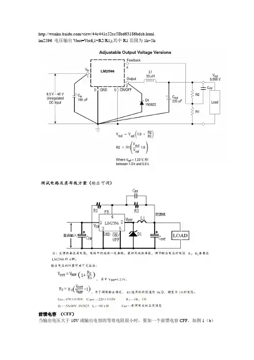
/view/44c441c52cc58bd63186bdab.html.lm2596 电压输出V out=Vref(1+R2/R1);其中R1范围为1k~5k前馈电容(CFF)当输出电压大于10V或输出电容的等效电阻很小时,要加一个前馈电容CFF,如图1(b)所示,这个电容是用来对反馈环路进行补偿和增加相位裕量以提高环路的稳定度。
对CFF 的选择,请参阅相关的设计步骤。
输出电容(COUT)这个电容是用来对输出滤波以及提高环路的稳定性,在设计开关调节器的应用中,必须使用小阻抗或低等效电阻(LOW ESR)的电解电容或固态钽电容。
在选择输出电容时,几个重要的参数是:(1)100KHz时的等效阻抗(ESR);(2)最大纹波电流均方根值;(3)耐压值;(4)标称容量。
吸纳二极管在LM2596的应用(调节器)中,需要一个吸纳二极管来为电感电流(当开关闭合时)提供通路,这必须是一个快速二极管且要靠近LM2596,管脚要短、相连接的导线也要短。
由于肖特基二极管开关速度快、正向压降小,所以,使用中其性能很好,特别是在输出电压低的应用中(5V或更低)。
超快恢复或高效整流二极管在使用中性能也很好。
但是在突然关闭时,可能会引起不稳定或电磁干扰。
电感的选择所有的调节器都有两种基本的工作方式:连续型和非连续型,两者之间的区别在于流过电感的电流的不同,或者是连续流过,或者是在一个开关周期内经过一段时间后变为0。
每一种工作模式都有可以影响调节器性能和需求的不同特点。
当负载电流很小时,许多设计中都采用非连续模式。
LM2596既可以用于连续型也可以用于非连续型。
1.电感的选择(L1)A.要根据图4、图5和图6所示的数据选择电感的适当值(分别对应输出电压为3.3V、5V 和12V),对于所有的其他输出电压的情况,请看输出可调的调节器的设计步骤。
B.在图4、图5和图6上,由最大输入电压线和最大负载电流线的交叉区域确定电感的值,每一个区域都对应一个电感值和一个电感代号(LXX)。
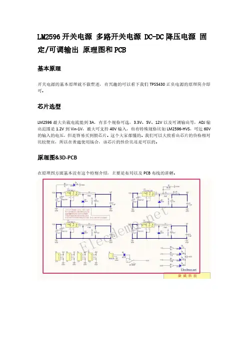
LM2596开关电源多路开关电源DC-DC降压电源固定/可调输出原理图和PCB基本原理开关电源的基本原理就不做赘述,有兴趣的可以看下我们TPS5430正负电源的原理简介即可。
芯片选型LM2596最大负载电流能到3A,有多个规格可选,3.3V、5V、12V以及可调输出等,ADJ输出范围是1.2V到Vin-1V,最大可支持40V输入,也有特殊规格比如LM2596-HVS,可达60V 的输入的电压,但是容易买到假芯片。
这个大家都懂的。
我们可以大致看出芯片的价格相对比较便宜,所以在普通使用场合,该芯片的性价比还是可以的。
原理图&3D-PCB在原理图方面基本没有这个特别介绍,主要是布局以及PCB布线的讲解。
具体讲解1、原理图需要注意电容以及二极管的方向,至于耐压、封装以及选型问题可以参考TPS5430开关电源分析。
2、这边截取了一路的布局以及走线作为示意。
首先C10和C12为电源输入滤波,应该尽量靠近芯片输入端,其次是输入的线应该尽量的粗,才能满足大电流。
3、芯片的第5脚是GND脚,需要在旁边放两个接地的过孔,这样有利于电流的释放接入背面的GND平面。
4、由于输出电流大是芯片发热就会比较厉害,所以在芯片散热焊盘的地方打了12个过孔方便散热。
5、其次是在接近输出端子的地方加一个C16电容可以进一步的减小纹波。
6、需要特别注意的是D5二极管为整流二极管,正向端接GND必须要良好接地,也就是需要过孔或者较粗的线接到输入电源的GND。
模块原理图-PDF、原理图库、PCB库下载以下为原文地址,https:///Elecdemo/article/details/103276839下载需要积分,仅供参考。
官方网址。
LM2596全中文资料随着电子技术的发展,各种电子设备越来越多,而其中一个重要的电源管理模块就是开关电源。
在电子设备中,开关电源起着将交流电转换为直流电的作用,提供稳定可靠的电力供应。
而LM2596是一种常见的开关稳压模块,它被广泛应用于各种电子设备中,提供高效、稳定的电源管理解决方案。
LM2596是一款具有高效率、低功耗和稳定性的降压型开关稳压模块。
它能够将输入电压转换为相对稳定的输出电压,通常被用于降低电源电压供应至微控制器、电路板、传感器等部件。
同时,LM2596还具备短路保护、过热保护等功能,以确保电子设备的安全运行。
LM2596采用了开关型调制控制技术,能够在不同负载情况下自动调整开关频率和占空比,以保持输出电压稳定。
它的输入电压范围广,可以适应不同的电源输入,包括交流电和直流电。
而输出电压可通过外部电阻分压调整,从而满足不同电子设备的需求。
除了稳压功能,LM2596还具备过流保护功能。
当电流超过设定值时,它会自动切断输出,避免因电流过大而损坏电子设备。
同时,LM2596还配备了过热保护功能,当温度超过一定范围时,它会自动降低工作频率或停止工作,以防止过热引起故障。
LM2596作为一种常见的开关稳压模块,其技术参数和应用案例都有详尽的中文资料可供参考。
对于初学者而言,这些资料不仅提供了LM2596的基本工作原理和使用方法,还介绍了它在各种电子设备中的具体应用场景和性能要求。
其中,电路图、元器件清单和详细的步骤说明,使得初学者能够更好地理解和使用LM2596。
此外,还有一些中文论坛和社区提供了关于LM2596的技术讨论和使用心得的帖子。
这些帖子通常包含了实际应用中遇到的问题和解决方案,对于学习和掌握LM2596的使用具有很大帮助。
在这些中文论坛中,你可以与其他电子爱好者交流经验,共同探讨LM2596的使用技巧。
综上所述,LM2596作为一种常见的开关稳压模块,提供了高效、稳定的电源管理解决方案。
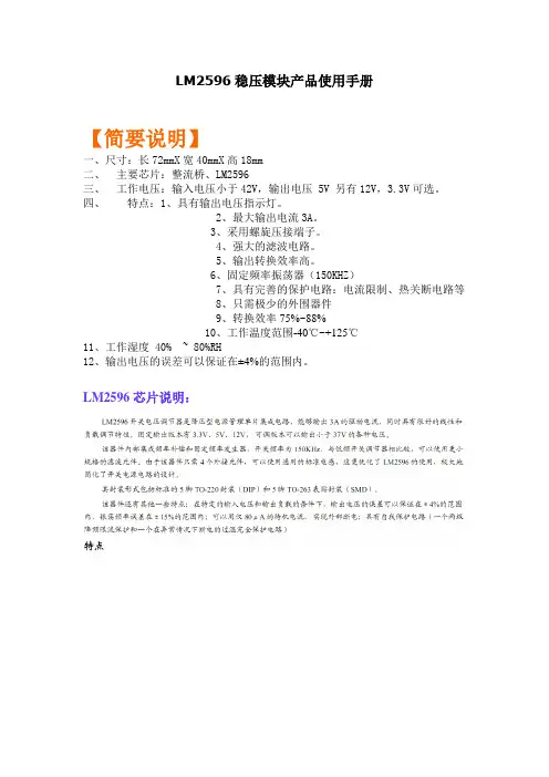
LM2596稳压模块产品使用手册
【简要说明】
一、尺寸:长72mmX宽40mmX高18mm
二、主要芯片:整流桥、LM2596
三、工作电压:输入电压小于42V,输出电压 5V 另有12V,3.3V可选。
四、特点:1、具有输出电压指示灯。
2、最大输出电流3A。
3、采用螺旋压接端子。
4、强大的滤波电路。
5、输出转换效率高。
6、固定频率振荡器(150KHZ)
7、具有完善的保护电路:电流限制、热关断电路等
8、只需极少的外围器件
9、转换效率75%~88%
10、工作温度范围-40℃~+125℃
11、工作湿度 40% ~ 80%RH
12、输出电压的误差可以保证在±4%的范围内。
LM2596芯片说明:
【标注说明】
【功能描述】
【原理图】
【PCB图】
【元件清单】
【应用举例1】
【应用举例2】
【图片展示】。
lm2596中文资料1. 概述lm2596是一款高效率开关电源稳压器芯片,广泛应用于电子设备中对直流电压进行稳定调整的场合。
本文档将详细介绍lm2596的特性、工作原理、应用场景以及使用注意事项。
2. 特性•宽输入电压范围:4V-40V•可调输出电压范围:1.23V-37V•高效率:可达到92%•最大输出电流:3A•过热保护功能3. 工作原理lm2596采用了开关稳压器的工作原理,通过周期性地开关和断开电流流通路径,将输入电压转换为稳定的输出电压。
其主要原理如下:1.输入电压通过电感和开关管传导到输出端,同时电容储存能量。
2.控制器检测输出电压,如果低于设定值,则控制开关管开启,使电流通过电感传输到输出端,提供稳定的输出电压。
3.如果输出电压高于设定值,则控制开关管关闭,切断电流流动。
这种周期性的开关和断开电路,可以通过控制开关管的开启时间和关闭时间,来调整输出电压的稳定性和精确度。
4. 应用场景lm2596广泛应用于各种需要稳定直流电压的场合,以下是lm2596常见的应用场景:4.1 电子设备稳压电源lm2596可以根据需要调整输出电压,可以在电子设备中作为稳压电源芯片使用。
它可以将输入电压调整为稳定的输出电压,以供电子设备正常运行。
4.2 LED照明由于lm2596具有高效率和可调输出电压的特性,非常适合用于LED照明应用。
lm2596可以将输入电压调整为适合LED灯的电压,提供稳定的电源以驱动LED照明。
4.3 高频电源lm2596的高效率和宽输入电压范围,使其非常适合用于高频电源应用。
lm2596可以将输入电压转换为稳定的高频输出,满足高频电源的需求。
5. 使用注意事项在使用lm2596时,请注意以下事项:1.输入电压不要超过40V,否则可能导致芯片过载损坏。
2.充分考虑散热问题,尽量避免芯片过热,建议在芯片周围预留散热空间。
3.在使用lm2596时,应按照芯片的使用说明进行正确的电路设计和连接。
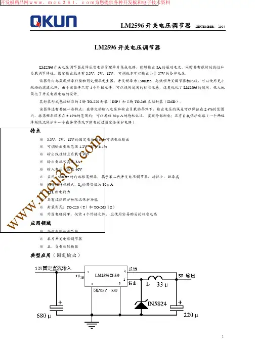
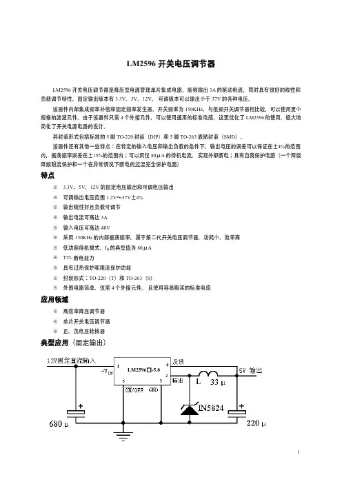
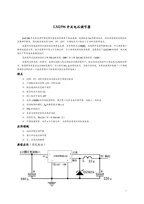
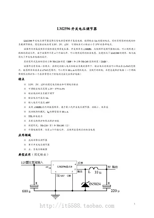
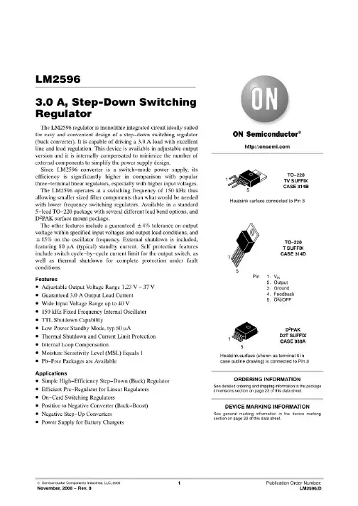
LM2596 开关电压调节器LM2596开关电压调节器是降压型电源管理单片集成电路,能够输出3A的驱动电流,同时具有很好的线性和负载调节特性。
固定输出版本有3.3V、5V、12V,可调版本可以输出小于37V的各种电压。
该器件内部集成频率补偿和固定频率发生器,开关频率为150KHz,与低频开关调节器相比较,可以使用更小规格的滤波元件。
由于该器件只需4个外接元件,可以使用通用的标准电感,这更优化了LM2596的使用,极大地简化了开关电源电路的设计。
其封装形式包括标准的5脚TO-220封装(DIP)和5脚TO-263表贴封装(SMD)。
该器件还有其他一些特点:在特定的输入电压和输出负载的条件下,输出电压的误差可以保证在±4%的范围内,振荡频率误差在±15%的范围内;可以用仅80μA的待机电流,实现外部断电;具有自我保护电路(一个两级降频限流保护和一个在异常情况下断电的过温完全保护电路)特点※ 3.3V、5V、12V的固定电压输出和可调电压输出※可调输出电压范围1.2V~37V±4%※输出线性好且负载可调节※输出电流可高达3A※输入电压可高达40V※采用150KHz的内部振荡频率,属于第二代开关电压调节器,功耗小、效率高※低功耗待机模式,I Q的典型值为80μA※TTL断电能力※具有过热保护和限流保护功能※封装形式:TO-220(T)和TO-263(S)※外围电路简单,仅需4个外接元件,且使用容易购买的标准电感应用领域※高效率降压调节器※单片开关电压调节器※正、负电压转换器典型应用(固定输出)LM2596□-5.0管脚图极限参数名称范围单位最大电源电压 45 V脚输入电压-0.3~25 V“反馈”脚电压 -0.3~25 V到地的输出电压(静态) -1 V功耗由内部限定 --储存温度 -65~150℃静电释放(人体放电1) 2000 V气流焊(60秒) 215 ℃ TO-263红外线焊接(10秒) 245 ℃ 焊接时的管脚温度TO-220 波峰焊/电烙铁焊接(10秒)260℃最高结温 150 ℃温度范围 -40~125℃工 作条 件电源电压 4.5~40 V注1:人体放电模式相当于一个100PF 的电容通过一个1.5K 的电阻向每个管脚放电。
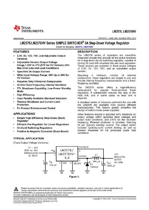
元器件交易网3.0A, 150Khz, Step-Down Switching RegulatorFEATURES3.3V, 5.0V, 12V, 15V, and Adjustable Output Versions Adjustable Version Output Voltage Range, 1.23 to 37V +/- 4%. Maximum Over Line and Load Conditions Guaranteed 3.0A Output Current Wide Input Voltage Range Requires Only 4 External Components 150Khz Fixed Frequency Internal Oscillator TTL Shutdown Capability, Low Power Standby Mode High Efficiency Uses Readily Available Standard Inductors Thermal Shutdown and Current Limit Protection Moisture Sensitivity Level(MSL) Equals1 TO-263(D2) TO-220V TO-220LM2596ApplicationsSimple High-Efficiency Step-Down(Buck) Regulator Efficient Pre-Regulator for Linear Regulators On-Card Switching Regulators Positive to Negative Converter(Buck-Boost) Negative Step-Up Converters Power Supply for Battery Chargers1. 2. 3. 4. 5. Vin Output Ground Feedback On/OffDESCRIPTIONThe LM2596 series of regulators are monolithic integrated circuits ideally suited for easy and convenient design of a step-down switching regualtor(buck converter). All circuits of this series are capable of driving a 3.0A load with excellent line and load regulation. These devices are available in fixed output voltages of 3.3V, 5.0V,12V, 15V, and an adjustable output version.ORDERING INFORMATIONDevice LM2596T-X.X LM2596TV-X.X LM2596R Marking LM2596T-X.X LM2596T-X.X LM2596R-X.X Package TO-220 TO-220V TO-263These regulatiors were designed to minimize the number of externalcomponents to simplify the power supply design. Standard series of inductors optimized for use with the LM2576 are offered by several different inductor manufacturers. Since the LM2596 converter is a switch-mode power supply, its efficiency is significantly higher in comparison with popular three-terminal limear reguators, especially with higher input voltages. In many cases, the power dissipated is so low that no heatsink is required or its size could be reduced dramatically. A standard series of inductors optimized for use with the LM2596 are available from several different manufacturers. This feature greatly simplifies the design of switch-mode power supplies. The LM2596 features include a guaranteed +/- 4% tolerance on output voltage within specified input voltages and output load conditions, and +/-15% on the oscillator frequency (+/- 2% over 0oC to 125 oC). External shutdown is included, featuring 80 uA(typical) standby current. The output switch includes cycle-bycycle current limiting, as well as thermal shutdown for full protection under fault conditions.HTC1Oct 2004 - Rev 0元器件交易网3.0A, 15V, Step-Down Switching RegulatorTypical Application (Fixed Output Voltage Versions)LM2596LM2596-5.033 uH680 uF1N5824220 uFFigure 1. Block Diagram and Typical ApplicationABSOLUTE MAXIMUM RATINGS(Absolute Maximum Ratings indicate limits beyond which damage to the device may occur.)Power DissipationTO-220, 5-LeadThermal Resistance, Junction-to-Ambient Thermal Resistance, Junction-to-caseTO-263Thermal Resistance, Junction-to-Ambient Thermal Resistance, Junction-to-caseHTC2Oct 2004 - Rev 0元器件交易网3.0A, 15V, Step-Down Switching RegulatorLM2596OPERATING RATINGS (Operating Ratings indicate conditions for which the device is intended to befunctional, but do not guarantee specific performance limits. For guaranteed specifications and test conditions, see the Electrical Characteristics.)ELECTRICAL CHARACTERISTICS / SYSTEM PARAMETERS ([Note 1] Test Circuit Figure 2) (Unless otherwise specified, Vin = 12 V for the 3.3 V, 5.0 V, and Adjustable version, Vin = 25 V for the 12 V version, and Vin = 30 V for the 15 V version. ILoad = 500 mA. For typical values TJ = 25°C, for min/max values TJ is the operating junction temperature range that applies [Note 2], unless otherwise noted.)LM2596-3.3 ([ Note 1]. Test Circuit Figure 2 )73 LM2596-5.0 ([ Note 1]. Test Circuit Figure 2 ) 180 LM2596-12 ([ Note 1]. Test Circuit Figure 2 )90 LM2596-15 ([ Note 1]. Test Circuit Figure 2 )98 LM2596-ADJ ([ Note 1]. Test Circuit Figure 2 )73HTC3Oct 2004 - Rev 0元器件交易网3.0A, 15V, Step-Down Switching RegulatorELECTRICAL CHARACTERISTICS / Device ParametersLM2596(Unless otherwise specified, Vin = 12 V for the 3.3 V, 5.0 V, and Adjustable version, Vin = 25 V for the 12 V version, and Vin = 30 V for the 15 V version. ILoad = 500 mA. For typical values Tj = 25°C, for min/max values Tj is the operating junction temperature range that applies [Note 2], unless otherwise noted.)10 0 127 110 15050 100 173 1731.16 01.4 1.53.6 3.4100 4.5 6.9 7.5 50 30 1002 5 00 2 0 2.0 2.0 2 V LOGIC = 2.5V (Regulator OFF) V LOGIC = 0.5V (Regulator ON) 5 0.02 1.3 1.32500.6 0.6 15 5.001. External components such as the catch diode, inductor, input and output capacitors can affect switching regulator system performance. When the LM2596 is used as shown in the Figure 1 test circuit, system performance will be as shown in system parameters section . 2. Tested junction temperature range for the LM2596 : TLOW = –0°C THIGH = +125°C 3. The oscillator frequency reduces to approximately 18 kHz in the event of an output short or an overload which causes the regulated output voltage to drop approximately 40% from the nominal output voltage. This self protection feature lowers the average dissipation of the IC by lowering the minimum duty cycle from 5% down to approximately 2%. 4. Output (Pin 2) sourcing current. No diode, inductor or capacitor connected to output pin. 5. Feedback (Pin 4) removed from output and connected to 0 V. 6. Feedback (Pin 4) removed from output and connected to +12 V for the Adjustable, 3.3 V, and 5.0V ersions, and +25 V for the 12 V and15 V versions, to force the output transistor “off”. 7. Vin = 40 V.HTC4Oct 2004 - Rev 0元器件交易网3.0A, 15V, Step-Down Switching RegulatorTYPICAL PERFORMANCE CHARACTERISTICS (Circuit of Figure 2)LM2596HTC5Oct 2004 - Rev 0元器件交易网3.0A, 15V, Step-Down Switching RegulatorTYPICAL PERFORMANCE CHARACTERISTICS (Circuit of Figure 2)Feedback Pin Bias CurrentLM2596HTC6Oct 2004 - Rev 0元器件交易网3.0A, 15V, Step-Down Switching RegulatorTest Circuit and Layout GuidelinesLM2596Figure 2. Typical Test Circuits and Layout GuideAs in any switching regulator, layout is very important. Rapidly switching currents associated with wiring inductance can generate voltage transients which can cause problems. For minimal inductance and ground loops, the wires indicated by heavy lines should be wide printed circuit traces and should be kept as short as possible. For best results, external components should be located as close to the switcher lC as possible using ground plane construction or single point grounding. If open core inductors are used, special care must be taken as to the location and positioning of this type of inductor. Allowing the inductor flux to intersect sensitive feedback, lC groundpath and COUT wiring can cause problems. When using the adjustable version, special care must be taken as to the location of the feedback resistors and the associated wiring. Physically locate both resistors near the IC, and route the wiring away from the inductor, especially an open core type of inductor.HTC7Oct 2004 - Rev 0元器件交易网3.0A, 15V, Step-Down Switching RegulatorLM2596PIN FUNCTION DESCRIPTION Symbol 1VinDescription This pin is the positive input supply for the LM2596 step–down switching23 45regulator.In order to minimize voltage transients and to supply the switching currents needed by the regulator, a suitable input bypass capacitor must be present .(Cin in Figure 1). Output This is the emitter of the internal switch. The saturation voltage Vsat of this output switch is typically 1.5 V. It should be kept in mind that the PCB area connected to this pin should be kept to a minimum in order to minimize coupling to sensitive circuitry. Circuit ground pin. See the information about the printed circuit board layout. Gnd Feedback This pin senses regulated output voltage to complete the feedback loop. The signal is divided by the internal resistor divider network R2, R1 and applied to the non–inverting input of the internal error amplifier. In the Adjustable version of the LM2596 switching regulator this pin is the direct input of the error amplifier and the resistor network R2, R1 is connected externally to allow programming of the output voltage. ON/OFF It allows the switching regulator circuit to be shut down using logic level signals, thus dropping the total input supply current to approximately 80 mA. The threshold voltage is typically 1.4 V. Applying a voltage above this value (up to +Vin) shuts the regulator off. If the voltage applied to this pin is lower than 1.4V or if this pin is left open, the regulator will be in the "on" conditionHTC8Oct 2004 - Rev 0元器件交易网3.0A, 15V, Step-Down Switching RegulatorLM2596PACKAGES DIMENSION : TO220-5LHTC9Oct 2004 - Rev 0元器件交易网3.0A, 15V, Step-Down Switching RegulatorPACKAGES DIMENSION : TO220V-5LLM2596HTC10Oct 2004 - Rev 0元器件交易网3.0A, 15V, Step-Down Switching RegulatorLM2596PACKAGES DIMENSION : TO263-5LHTC11Oct 2004 - Rev 0。
LM2596电源降压调整器(150KHz,3A)英文文章名:LM2596 SIMPLE SWITCHER® Power Converter 150 kHz3A Step-Down Voltage Regulator文章出处:版本号:DS012583 日期:2002年5月摘录人:黄明强摘录日期:2007年5月3日是否好买估计:生产中心正在使用价格:概述:LM2596系列开关电压调节器是降压型电源管理单片集成电路,能够输出3A的驱动电流,同时具有很好的线性和负载调节特性。
固定输出版本有3.3V、5V、12V,还有一个输出可调版本。
添加少量的外部元件就可以使用该电压调节器。
该器件内部集成有频率补偿和固定频率发生器。
开关频率为150KHz,与低频开关调节器相比较,可以使用更小规格的滤波元件。
其封装形式包括标准的5脚TO-220封装和5脚TO-263表贴封装。
由于该器件可以使用通用的标准电感,这更优化了LM2596的使用,极大地简化了开关电源电路的设计。
该器件还有其他一些特点:在特定的输入电压和输出负载的条件下,输出电压的误差可以保证在±4%的范围内,振荡频率误差在±15%的范围内;可以用仅80μA的待机电流,实现外部断电;具有自我保护电路(一个两级降频限流保护和一个在异常情况下断电的过温完全保护电路)。
特征:※ 3.3V、5V、12V的固定电压输出和可调电压输出※可调输出电压范围1.2V~37V,±4%※封装形式:TO-220(T)和TO-263(S)※保证输出负载电流3A※输入电压可高达40V※仅需4个外接元件※很好的线性和负载调节特性※150KHz固定频率的内部振荡器※TTL关断能力※低功耗待机模式,I Q的典型值为80μA※高转换效率※使用容易购买的标准电感※具有过热保护和限流保护功能应用:※简易高效率降压调节器※在卡上的开关电压调节器※正到负电压转换器专利号:5382918典型电路(固定输出电压版本):封装和型号:※弯曲交叉的引脚,通孔封装,5脚TO-220 (T)订货型号:LM2596T-3.3, LM2596T-5.0,LM2596T-12 or LM2596T-ADJ ※表面贴封装,5脚TO-263 (S)订货型号:LM2596S-3.3, LM2596S-5.0, LM2596S-12 or LM2596S-ADJ 极限条件:最大供电电压45VON /OFF 管脚输入电压-0.3≤V≤+25V反馈脚电压-0.3≤V≤+25V输出电压到地(稳态)-1V功率消耗内部限定储存温度-65°C 到+150°CESD易感性(人体模式)2KV焊接温度T封装(锡焊, 10秒) +260°C最大结温+150°C运行条件:温度范围-40°C≤T J≤+125°C供电电压 4.5V 到40VLM2596-3.3电参数说明:标准字体对应的项目适合于TJ=25℃时,粗体字对应的项目适合于全温度范围LM2596-5.0电参数说明:标准字体对应的项目适合于TJ=25℃时,粗体字对应的项目适合于全温度范围LM2596-12电参数所有输出电压版本电参数说明:标准字体对应的项目适合于TJ=25℃时,带下划线的粗斜体字对应的项目适合于整个温度范围。