FPGA可编程逻辑器件芯片XC5VLX155T-1FFG1136C中文规格书
- 格式:pdf
- 大小:383.90 KB
- 文档页数:5

© 2006–2010, 2014, 2016 Xilinx, Inc. Xilinx, the Xilinx logo, Artix, ISE, Kintex, Spartan, Virtex, Vivado, Zynq, and other designated brands included herein are trademarks of Xilinx in the United States and other countries. PowerPC is a trademark of IBM Corp. and is used under license. PCI, PCI Express, PCIe, and PCI-X are trademarks of PCI-SIG. All other trademarks are the property of their respective owners.Virtex-5 FPGA Electrical CharacteristicsVirtex®-5 FPGAs are available in -3, -2, -1 speed grades, with -3 having the highest performance. Virtex-5 FPGA DC and AC characteristics are specified for both commercial and industrial grades. Except the operating temperature range or unless otherwise noted, all the DC and ACelectrical parameters are the same for a particular speed grade (that is, the timing characteristics of a -1 speed grade industrial device are the same as for a -1 speed grade commercial device). However, only selected speed grades and/or devices might be available in the industrial range.All supply voltage and junction temperature specifications are representative of worst-case conditions. Theparameters included are common to popular designs and typical applications.This Virtex-5 FPGA data sheet, part of an overall set of documentation on the Virtex-5 family of FPGAs, is available on the Xilinx website:•Virtex-5 Family Overview •Virtex-5 FPGA User Guide•Virtex-5 FPGA Configuration Guide•Virtex-5 FPGA XtremeDSP™ Design Considerations •Virtex-5 FPGA Packaging and Pinout Specification•Embedded Processor Block in Virtex-5 FPGAs Reference Guide•Virtex-5 FPGA RocketIO™ GTP Transceiver User Guide •Virtex-5 FPGA RocketIO GTX Transceiver User Guide •Virtex-5 FPGA Embedded Tri-Mode Ethernet MAC User Guide•Virtex-5 FPGA Integrated Endpoint Block User Guide for PCI Express® Designs•Virtex-5 FPGA System Monitor User Guide •Virtex-5 FPGA PCB Designer’s GuideAll specifications are subject to change without notice.Virtex-5 FPGA DC CharacteristicsProduct SpecificationTable 1:Absolute Maximum RatingsSymbol DescriptionUnits V CCINT Internal supply voltage relative to GND –0.5 to 1.1V V CCAUX Auxiliary supply voltage relative to GND–0.5 to 3.0V V CCO Output drivers supply voltage relative to GND –0.5 to 3.75V V BATT Key memory battery backup supply –0.5 to 4.05V V REFInput reference voltage–0.5 to 3.75V V IN (3)3.3V I/O input voltage relative to GND (4) (user and dedicated I/Os)–0.75 to 4.05V 3.3V I/O input voltage relative to GND (restricted to maximum of 100 user I/Os)(5)–0.95 to 4.4(Commercial Temperature)V –0.85 to 4.3(Industrial Temperature)2.5V or below I/O input voltage relative to GND (user and dedicated I/Os)–0.75 to V CCO +0.5V I IN Current applied to an I/O pin, powered or unpowered±100mA Total current applied to all I/O pins, powered or unpowered±100mA V TS Voltage applied to 3-state 3.3V output (4) (user and dedicated I/Os)–0.75 to 4.05V Voltage applied to 3-state 2.5V or below output (user and dedicated I/Os)–0.75 to V CCO +0.5V T STG Storage temperature (ambient)–65to 150°C T SOL Maximum soldering temperature (2)+220°C T JMaximum junction temperature (2)+125°CNotes:1.Stresses beyond those listed under Absolute Maximum Ratings might cause permanent damage to the device. These are stress ratings only, andfunctional operation of the device at these or any other conditions beyond those listed under Operating Conditions is not implied. Exposure to Absolute Maximum Ratings conditions for extended periods of time might affect device reliability.2.For soldering guidelines, refer to UG112: Device Package User Guide . For thermal considerations, refer to UG195: Virtex-5 FPGA Packaging andPinout Specification on the Xilinx website.3. 3.3V I/O absolute maximum limit applied to DC and AC signals.4.For 3.3V I/O operation, refer to UG190: Virtex-5 FPGA User Guide, Chapter 6, 3.3V I/O Design Guidelines .5.For more flexibility in specific designs, a maximum of 100 user I/Os can be stressed beyond the normal specification for no more than 20% of a data period .找FPGA和CPLD可编程逻辑器件,上深圳宇航军工半导体有限公司DS202 (v5.5) June 17, 2016Table 2:Recommended Operating ConditionsSymbol DescriptionTemperature RangeMin Max Units V CCINT Internal supply voltage relative to GND, T J =0°C to +85°C Commercial 0.95 1.05V Internal supply voltage relative to GND, T J =–40°C to +100°C Industrial 0.95 1.05V V CCAUX (1)Auxiliary supply voltage relative to GND, T J =0°C to +85°C Commercial 2.375 2.625V Auxiliary supply voltage relative to GND, T J =–40°C to +100°C Industrial 2.375 2.625V V CCO (2,4,5)Supply voltage relative to GND, T J =0°C to +85°C Commercial 1.14 3.45V Supply voltage relative to GND, T J =–40°C to +100°C Industrial 1.14 3.45V V IN3.3V supply voltage relative to GND, T J =0°C to +85°C Commercial GND –0.20 3.45V 3.3V supply voltage relative to GND, T J =–40°C to +100°C Industrial GND –0.20 3.45V 2.5V and below supply voltage relative to GND, T J =0°C to +85°CCommercial GND –0.20V CCO +0.2V 2.5V and below supply voltage relative to GND, T J =–40°C to +100°CIndustrial GND –0.20V CCO +0.2V I IN (6)Maximum current through any pin in a powered or unpowered bank when forward biasing the clamp diode Commercial 10mA Industrial 10mA V BATT (3)Battery voltage relative to GND, T J =0°C to +85°C Commercial 1.0 3.6V Battery voltage relative to GND, T J =–40°C to +100°CIndustrial1.03.6VGTX_DUAL Tile SpecificationsGTX_DUAL Tile DC CharacteristicsTable 36:Absolute Maximum Ratings for GTX_DUAL TilesSymbol Description Units MGTAVCCPLL Analog supply voltage for the GTX_DUAL shared PLL relative to GND–0.5 to 1.1V MGTAVTTTX Analog supply voltage for the GTX_DUAL transmitters relative to GND–0.5 to 1.32V MGTAVTTRX Analog supply voltage for the GTX_DUAL receivers relative to GND–0.5 to 1.32V MGTAVCC Analog supply voltage for the GTX_DUAL common circuits relative to GND–0.5 to 1.1V–0.5 to 1.32V MGTAVTTRXC Analog supply voltage for the resistor calibration circuit of the GTX_DUALcolumnSystem Monitor Analog-to-Digital Converter SpecificationTable 51:Analog-to-Digital SpecificationsParameter Symbol Comments/Conditions Min Typ Max UnitsAV DD=2.5V±2%, V REFP=2.5V,V REFN=0V, ADCCLK=5.2MHz, T A=T MIN to T MAX, Typical values at T A=+25°CDC Accuracy: All external input channels such as V P/V N and V AUXP[15:0]/V AUXN[15:0], Unipolar Mode,and Common Mode = 0VResolution10Bits Integral Nonlinearity INL±2LSBsDifferential Nonlinearity DNL No missing codes (T MIN to T MAX)Guaranteed Monotonic±0.9LSBs Unipolar Offset Error(1)Uncalibrated±2±30LSBs Bipolar Offset Error(1)Uncalibrated measured in bipolar mode ±2±30LSBs Gain Error(1)Uncalibrated±0.2±2% Bipolar Gain Error(1)Uncalibrated measured in bipolar mode±0.2±2%Total Unadjusted Error (Uncalibrated)TUE Deviation from ideal transfer function.V REFP–V REFN=2.5V±10LSBsTotal Unadjusted Error (Calibrated)TUE Deviation from ideal transfer function.V REFP–V REFN=2.5V±1±2LSBsCalibrated Gain TemperatureCoefficientVariation of FS code with temperature±0.01LSB/°CDC Common-Mode Reject CMRR DC V N = V CM=0.5V± 0.5V,V P–V N=100mV70dB Conversion Rate(2)Conversion Time - Continuous t CONV Number of CLK cycles2632Conversion Time - Event t CONV Number of CLK cycles21T/H Acquisition Time t ACQ Number of CLK cycles4DRP Clock Frequency DCLK DRP clock frequency8250MHz ADC Clock Frequency ADCCLK Derived from DCLK1 5.2MHz CLK Duty cycle4060% Analog Inputs(3)Dedicated Analog Inputs Input Voltage RangeV P - V N Unipolar Operation01Volts Differential Inputs–0.25+0.25Unipolar Common Mode Range (FS input)0+0.5 Differential Common Mode Range (FS input) +0.3+0.7 Bandwidth20MHzAuxiliary Analog InputsInput Voltage RangeV AUXP[0] /V AUXN[0] to V AUXP[15] /V AUXN[15]Unipolar Operation01Volts Differential Operation–0.25+0.25Unipolar Common Mode Range (FS input)0+0.5 Differential Common Mode Range (FS input)+0.3+0.7 Bandwidth10kHzInput Leakage Current A/D not converting, ADCCLK stopped±1.0µA Input Capacitance10pFOn-chip Supply Monitor Error V CCINT and V CCAUX with calibration enabled±1.0% Reading On-chip Temperature MonitorError–40°C to +125°C with calibration enabled±4°C。

General DescriptionThe Defense-grade XQ UltraScale™ architecture-based devices extend the equivalent commercial offerings, adding unique ruggedized packages, extended operating temperature range support, and added environmental qualification testing. This XQ portfolio spans the following families, with each offering a unique mix of features. XQ Kintex® UltraScale FPGAs: High-performance FPGAs with a focus on price/performance, using both monolithic andnext-generation stacked silicon interconnect (SSI) technology. High DSP and block RAM-to-logic ratios and next-generation transceivers, combined with low-cost packaging, enable an optimum blend of capability and cost.XQ Kintex UltraScale+™ FPGAs: Increased performance and on-chip UltraRAM memory to reduce BOM cost. The ideal mix of high-performance peripherals and cost-effective system implementation. Kintex UltraScale+ FPGAs have numerous power options that deliver the optimal balance between the required system performance and the smallest power envelope.XQ Virtex® UltraScale+ FPGAs: The highest transceiver bandwidth, highest DSP count, and highest on-chip and in-package memory available in the UltraScale architecture. Virtex UltraScale+ FPGAs also provide numerous power options that deliver the optimal balance between the required system performance and the smallest power envelope.XQ Zynq® UltraScale+ MPSoCs: Combine the Arm® v8-based Cortex®-A53 high-performance energy-efficient 64-bit application processor with the Arm Cortex-R5 real-time processor and the UltraScale architecture to create the industry's first Defense-grade MPSoCs. Provide unprecedented power savings, heterogeneous processing, and programmable acceleration. XQ Zynq UltraScale+ RFSoCs: Combine RF data converter subsystem and forward error correction with industry-leading programmable logic and heterogeneous processing capability. Integrated RF-ADCs, RF-DACs, and soft-decision FECs (SD-FEC) provide the key subsystems for multiband, multi-mode cellular radios and cable infrastructure.XQ Device ComparisonsDS895 (v2.0) November 15, 2018Product Specification Table 1:Device Resources(1)XQ Kintex UltraScale FPGAXQ KintexUltraScale+FPGAXQ VirtexUltraScale+FPGAXQ ZynqUltraScale+MPSoCXQ ZynqUltraScale+RFSoCMPSoC Processing System✓✓RF-ADC/DAC and SD-FEC✓System Logic Cells (K)530–1,451475–1,143862–2,835154–1,143930 Block Memory (Mb)21.1–75.916.9–34.625.3–70.9 5.1–34.638.0 UltraRAM (Mb)18–3690–2700–3622.5 HBM DRAM (GB)0(2)DSP (Slices)1,920–5,5201,824–1,9682,280–9,216360–3,5284,272 DSP Performance (GMAC/s)(3)7,2973,05014,2845,4686,621 Transceivers16–6416–5640–960–488–16 Max. Transceiver Speed (Gb/s)16.328.228.228.228.2 Max. Serial Bandwidth (full duplex) (Gb/s)2,0862,4025,4161,950902I/O Pins312–728280–512416–83282–644152–408 Notes:1.Metrics given in this table pertain to the XQ ruggedized package devices. For non-ruggedized device variants consult Xilinx sales.2.HBM not currently offered in an XQ ruggedized Package; consult Xilinx sales for further details and options.3.Calculated based on XQ maximum DSP clock rate for a Symmetric FIR Filter, e.g. for KU040 with 1920 DSP48s, -2 speed-grade DSP48F MAX=661MHz, GMACs=2x0.661x1,920=2,538.XQ Kintex UltraScaleXQ Kintex UltraScale+XQ Virtex UltraScale+XQ Zynq UltraScale+ PLXQ Zynq UltraScale+ PSADC10-bit 200kSPS10-bit 200kSPS10-bit 1MSPS Interfaces JTAG, I2C, DRP JTAG, I2C, DRP, PMBus APB•64-bit quad-core Arm Cortex-A53 MPCores. Features associated with each core include: o Arm v8-A Architectureo Operating target frequency: up to 1.5GHzo Single and double precision floating point:4SP/2DP FLOPso NEON Advanced SIMD support with single and double precision floating point instructions o A64 instruction set in 64-bit operating mode, A32/T32 instruction set in 32-bit operating mode o Level 1 cache (separate instruction and data, 32KB each for each Cortex-A53 CPU)–2-way set-associative Instruction Cache with parity support–4-way set-associative Data Cache with ECC supporto Integrated memory management unit (MMU) per processor coreMIO OverviewThe IOP peripherals communicate to external devices through a shared pool of up to 78 dedicated multiplexed I/O (MIO) pins. Each peripheral can be assigned one of several pre-defined groups of pins, enabling a flexible assignment of multiple devices simultaneously. Although 78 pins are not enough for simultaneous use of all the I/O peripherals, most IOP interface signals are available to the PL, allowing use of standard PL I/O pins when powered up and properly configured. Extended multiplexed I/O (EMIO) allows unmapped PS peripherals to access PL I/O.Port mappings can appear in multiple locations. For example, there are up to 12 possible port mappings for CAN pins. The PS Configuration Wizard (PCW) tool aids in peripheral and static memory pin mapping. See Table 17.Transceiver (PS-GTR)The four PS-GTR transceivers, which reside in the full power domain (FPD), support data rates of up to 6.0Gb/s. All the protocols cannot be pinned out at the same time. At any given time, four differential pairs can be pinned out using the transceivers. This is user programmable via the high-speed I/O multiplexer (HS-MIO). •A Quad transceiver PS-GTR (TX/RX pair) able to support following standards simultaneouslyo x1, x2, or x4 lane of PCIe at Gen1 (2.5Gb/s) or Gen2 (5.0Gb/s) rates o 1 or 2 lanes of DisplayPort (TX only) at 1.62Gb/s, 2.7Gb/s, or 5.4Gb/s o 1 or 2 SATA channels at 1.5Gb/s, 3.0Gb/s, or 6.0Gb/s o 1 or 2 USB3.0 channels at 5.0Gb/s o1-4 Ethernet SGMII channels at 1.25Gb/sTable 17:MIO Peripheral Interface MappingPeripheral InterfaceMIOEMIOQuad-SPI NAND YesNo USB2.0: 0,1Yes: External PHY No SDIO 0,1Yes Yes SPI: 0,1I2C: 0,1CAN: 0,1GPIOYesCAN: External PHY GPIO: Up to 78 bits YesCAN: External PHY GPIO: Up to 96 bitsGigE: 0,1,2,3RGMII v2.0: External PHYSupports GMII, RGMII v2.0 (HSTL), RGMII v1.3, MII, SGMII, and 1000BASE-X in Programmable LogicUART: 0,1Simple UART:Only two pins (TX and RX)Full UART (TX, RX, DTR, DCD, DSR, RI, RTS, and CTS) requires either:•Two Processing System (PS) pins (RX and TX) through MIO and sixadditional Programmable Logic (PL) pins, or •Eight Programmable Logic (PL) pinsDebug Trace Ports Yes: Up to 16 trace bits Yes: Up to 32 trace bits Processor JTAGYesYes。
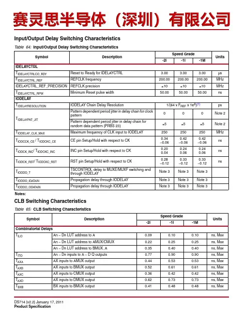
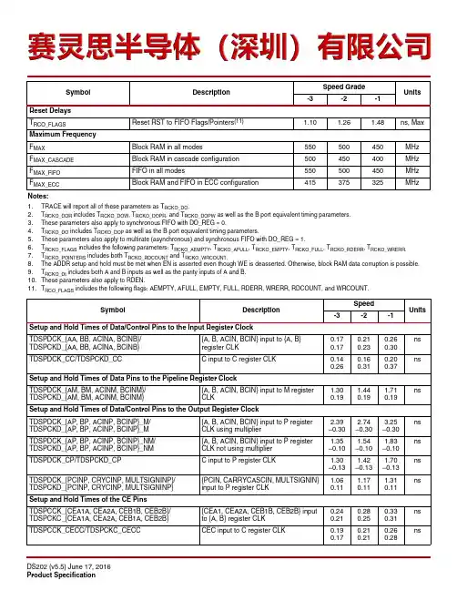
Input/Output Delay Switching CharacteristicsCLB Switching CharacteristicsTable 64:Input/Output Delay Switching CharacteristicsSymbolDescriptionSpeed Grade Units-2I-1I-1MIDELAYCTRL T IDELAYCTRLCO_RDY Reset to Ready for IDELAYCTRL 3.00 3.00 3.00µs F IDELAYCTRL_REF REFCLK frequency 200.00200.00200.00MHz IDELAYCTRL_REF_PRECISION REFCLK precision±10±10±10MHz T IDELAYCTRL_RPW Minimum Reset pulse width50.0050.0050.00nsIODELAYT IDELAYRESOLUTIONIODELAY Chain Delay Resolution1/(64x F REF x 1e 6)(1)ps T IDELAYP AT_JITPattern dependent period jitter in delay chain for clock pattern000Note 2Pattern dependent period jitter in delay chain for random data pattern (PRBS 23)±5±5±5Note 2T IODELAY_CLK_MAX Maximum frequency of CLK input to IODELAY 250250250MHz T IODCCK_CE / T IODCKC_CE CE pin Setup/Hold with respect to CK 0.34–0.060.42–0.060.42–0.06ns T IODCK_INC / T IODCKC_INC INC pin Setup/Hold with respect to CK 0.200.040.240.060.240.06ns T IODCK_RST / T IODCKC_RST RST pin Setup/Hold with respect to CK0.28–0.120.33–0.120.33–0.12nsT IODDO_T TSCONTROL delay to MUXE/MUXF switching and through IODELAYNote 3Note 3Note 3T IODDO_IDA TAIN Propagation delay through IODELAY Note 3Note 3Note 3T IODDO_ODA TAIN Propagation delay through IODELAYNote 3Note 3Note 3Notes:Table 65:CLB Switching CharacteristicsSymbol DescriptionSpeed GradeUnits-2I-1I-1MCombinatorial Delays T ILOAn –Dn LUT address to A0.090.100.10ns, Max An –Dn LUT address to AMUX/CMUX 0.220.250.25ns, Max An –Dn LUT address to BMUX_A0.350.400.40ns, Max T ITO An –Dn inputs to A –D Q outputs 0.770.900.90ns, Max T AXA AX inputs to AMUX output 0.440.530.53ns, Max T AXB AX inputs to BMUX output 0.520.610.61ns, Max T AXC AX inputs to CMUX output 0.360.420.42ns, Max T AXD AX inputs to DMUX output 0.620.730.73ns, Max T BXBBX inputs to BMUX output0.410.480.48ns, MaxCLB Distributed RAM Switching Characteristics (SLICEM Only)CLB Shift Register Switching Characteristics (SLICEM Only)Table 66:CLB Distributed RAM Switching CharacteristicsSymbol DescriptionSpeed GradeUnits-2I-1I-1MSequential Delays T SHCKO Clock to A –B outputs1.26 1.54 1.54ns, Max T SHCKO_1Clock to AMUX –BMUX outputs1.381.681.68ns, MaxSetup and Hold Times Before/After Clock CLK T DS /T DH A –D inputs to CLK 0.840.22 1.030.26 1.030.26ns, Min T AS /T AH Address An inputs to clock 0.460.220.540.270.540.27ns, Min T WS /T WH WE input to clock 0.39–0.040.46–0.020.46–0.02ns, Min T CECK /T CKCECE input to CLK0.42–0.070.51–0.060.51–0.06ns, MinClock CLK T MPW Minimum pulse width 0.82 1.00 1.00ns, Min T MCP Minimum clock period1.642.002.00ns, MinNotes:1. A Zero “0” Hold Time listing indicates no hold time or a negative hold time. Negative values cannot be guaranteed “best-case”, but if a “0” is listed, there is no positive hold time.2.T SHCKO also represents the CLK to XMUX output. Refer to TRACE report for the CLK to XMUX path.Table 67:CLB Shift Register Switching CharacteristicsSymbolDescriptionSpeed GradeUnits-2I-1I-1MSequential Delays T REG Clock to A –D outputs 1.43 1.73 1.73ns, Max T REG_MUX Clock to AMUX –DMUX output 1.55 1.87 1.87ns, Max T REG_M31Clock to DMUX output via M31 output1.151.381.38ns, MaxSetup and Hold Times Before/After Clock CLK T WS /T WH WE input 0.24–0.040.29–0.020.29–0.02ns, Min T CECK /T CKCE CE input to CLK 0.27–0.070.33–0.060.33–0.06ns, Min T DS /T DH A –D inputs to CLK0.660.090.780.110.780.11ns, MinClock CLK T MPW Minimum pulse width 0.700.850.85ns, MinNotes:1.A Zero “0” Hold Time listing indicates no hold time or a negative hold time. Negative values cannot be guaranteed “best-case”, but if a “0” is listed, there is no positive hold time.Block RAM and FIFO Switching Characteristics Table 68:Block RAM and FIFO Switching CharacteristicsSymbol DescriptionSpeed GradeUnits -2I-1I-1MBlock RAM and FIFO Clock to Out DelaysT RCKO_DO and T RCKO_DOR(1)Clock CLK to DOUT output (without output register)(2)(3) 1.92 2.19 2.19ns, MaxClock CLK to DOUT output (with output register)(4)(5)0.690.820.82ns, MaxClock CLK to DOUT output with ECC (without outputregister)(2)(3)3.03 3.61 3.61ns, MaxClock CLK to DOUT output with ECC (with outputregister)(4)(5)0.770.930.93ns, MaxClock CLK to DOUT output with Cascade (without outputregister)(2)2.44 2.94 2.94ns, MaxClock CLK to DOUT output with Cascade (with outputregister)(4)1.07 1.30 1.30ns, Max T RCKO_FLAGS Clock CLK to FIFO flags outputs(6)0.87 1.02 1.02ns, Max T RCKO_POINTERS Clock CLK to FIFO pointer outputs(7) 1.26 1.48 1.48ns, Max T RCKO_ECCR Clock CLK to BITERR (with output register)0.770.930.93ns, Max T RCKO_ECC Clock CLK to BITERR (without output register)2.853.41 3.41ns, MaxClock CLK to ECCP ARITY in standard ECC mode 1.47 1.74 1.74ns, MaxClock CLK to ECCP ARITY in ECC encode only mode0.89 1.05 1.05ns, Max Setup and Hold Times Before/After Clock CLKT RCCK_ADDR/T RCKC_ADDR ADDR inputs(8)0.400.320.480.360.480.36ns, MinT RDCK_DI/T RCKD_DI DIN inputs(9)0.300.280.350.290.350.29ns, MinT RDCK_DI_ECC/T RCKD_DI_ECC DIN inputs with ECC in standard mode(9)0.370.330.420.360.420.47ns, Min DIN inputs with ECC encode only(9)0.720.330.770.360.770.47ns, MinT RCCK_EN/T RCKC_EN Block RAM Enable (EN) input 0.360.150.420.150.420.15ns, MinT RCCK_REGCE/T RCKC_REGCE CE input of output register 0.160.240.180.270.180.27ns, MinT RCCK_SSR/T RCKC_SSR Synchronous Set/ Reset (SSR) input 0.210.250.260.280.260.28ns, MinT RCCK_WE/T RCKC_WE Write Enable (WE) input 0.510.170.630.180.630.18ns, MinT RCCK_WREN/T RCKC_WREN WREN/RDEN FIFO inputs(10)0.410.340.480.400.480.40ns, MinReset DelaysT RCO_FLAGS Reset RST to FIFO Flags/Pointers(11) 1.26 1.48 1.48ns, MaxBPI Master Flash Mode Programming Switching T BPICCO (4)ADDR[25:0], RS[1:0], FCS_B, FOE_B, FWE_B outputs valid after CCLK rising edge101010ns T BPIDCC /T BPICCD Setup/Hold on D[15:0] data input pins3.00.5 3.00.5 3.00.5ns T INITADDRMinimum period of initial ADDR[25:0] address cycles3.03.03.0CCLK cyclesSPI Master Flash Mode Programming Switching T SPIDCC /T SPIDCCD DIN Setup/Hold before/after the rising CCLK edge 4.00.0 4.00.0 5.00.0ns T SPICCM MOSI clock to out 101010ns T SPICCFC FCS_B clock to out101010ns T FSINIT /T FSINITHFS[2:0] to INIT_B rising edge Setup and Hold222µsCCLK Output (Master Modes)T MCCKL Master CCLK clock minimum Low time 3.0 3.0 3.0ns, Min T MCCKHMaster CCLK clock minimum High time3.03.03.0ns, MinCCLK Input (Slave Modes)T SCCKL Slave CCLK clock minimum Low time 2.0 2.0 2.0ns, Min T SCCKH Slave CCLK clock minimum High time2.02.02.0ns, MinDynamic Reconfiguration Port (DRP) for DCM and PLL Before and After DCLKF DCKMaximum frequency for DCLK 450400400MHz T DMCCK_DADDR /T DMCKC_DADDR DADDR Setup/Hold 1.350.0 1.560.0 1.560.0ns T DMCCK_DI /T DMCKC_DI DI Setup/Hold 1.350.0 1.560.0 1.560.0ns T DMCCK_DEN /T DMCKC_DEN DEN Setup/Hold time 1.350.0 1.560.0 1.560.0ns T DMCCK_DWE /T DMCKC_DWE DWE Setup/Hold time 1.350.0 1.560.0 1.560.0ns T DMCKO_DO CLK to out of DO (3) 1.12 1.30 1.30ns T DMCKO_DRDY CLK to out of DRDY1.121.301.30nsNotes:1.Maximum frequency and setup/hold timing parameters are for 3.3V and2.5V configuration voltages.2.T o support longer delays in configuration, use the design solutions described in the Virtex-5 FPGA User Guide .3.DO will hold until next DRP operation.4.Only during configuration, the last edge is determined by a weak pull-up/pull-down resistor in the I/O.Table 70:Configuration Switching Characteristics (Cont’d)SymbolDescriptionSpeed Grade Units-2I-1I-1MSymbolDescriptionDevicesSpeed Grade Units -2I -1I -1M T BCCCK_CE /T BCCKC_CE (1)CE pins Setup/Hold All 0.270.000.310.000.310.00ns T BCCCK_S /T BCCKC_S (1)S pins Setup/HoldAll0.270.000.310.000.310.00ns T BCCKO_O (2)BUFGCTRL delay from I0/I1 to OLX30T, LX85, LX110, LX110T, SX50T , FX70T , FX100T , and FX130T 0.220.250.25nsLX155T0.140.30N/A ns LX220T, LX330T, SX95T , SX240T, and FX200T0.220.25N/AnsMaximum FrequencyF MAXGlobal clock tree (BUFG)LX30T, LX85, LX110, LX110T, SX50T , and FX70T(I)667600N/A MHz LX155T, FX70T(M), and FX100T 600550550MHz FX130T500450N/A MHz LX220T, LX330T, SX95T , SX240T, and FX200T500450N/AMHz。
XCN11031 (v1.1) June 9, 2015 Product Discontinuation NoticeOverviewThe purpose of this notification is to inform Xilinx customers of the discontinuation of certain Virtex®-4 andVirtex®-5 FPGA devices special part numbers only; devices will continue to ship without change to form, fit, or function, but with updated part numbers.DescriptionSince the introduction of Virtex-4 and Virtex-5 FPGA products, Xilinx has qualified both product families in both Toshiba, in Oita, Japan, and UMC in Taiwan, and has been shipping the majority of devices in each product family from UMC. As part of the consolidation effort described in XCN11030, wafer fabrication for all Virtex-4 and Virtex-5 Devices described in this document will be transferred to UMC.As a result of this transfer, certain part numbers, including SCD and Stepping, will be converted into standard part numbers.For these devices, there is no change to the form, fit, or function of the devices themselves. Qualification data is available in the Xilinx reliability report UG116.Products AffectedThe products affected include all Virtex-4 and Virtex-5 part numbers associated with the following associated SCD and stepping: 0641, 0988, 4009, 4013, 4023, 4058, 4094, 4098, 4108, CS1, CS2 part numbers listed in Table 1, Table 2 and Table 3 below.*Xilinx may cross ship from Toshiba or UMC until Toshiba inventory is depletedXCN11031 (v1.1) June 9, 2015Product Discontinuation Notice For Virtex-4 and Virtex-5 FPGA SCDs from Toshiba Wafer FabricationXCN11031 (v1.1) June 9, 2015Product Discontinuation Notice For Virtex-4 and Virtex-5 FPGA SCDs from Toshiba Wafer FabricationXCN11031 (v1.1) June 9, 2015Product Discontinuation Notice For Virtex-4 and Virtex-5 FPGA SCDs from Toshiba Wafer FabricationXCN11031 (v1.1) June 9, 2015Product Discontinuation Notice For Virtex-4 and Virtex-5 FPGA SCDs from Toshiba Wafer FabricationXCN11031 (v1.1) June 9, 2015。

Chapter 10:GTX-to-Board InterfaceFully Unused ColumnTable10-13 shows the configuration for Use Case 8, where:• A GTX_DUAL tile is unused•Both transceivers are unused•Boundary-Scan is not functioningTable 10-13:Use Case 8Pin or Pin Pair Connect To FilterMGTRXP/MGTRXN GND-MGTTXP/MGTTXN Floating, no connection-MGTREFCLKP/MGTREFCLKN Floating, no connection-MGTAVTTTX GND-MGTAVTTRX GND-MGTAVTTRXC Floating, no connection-MGTAVCCPLL GND-MGTAVCC GND-MGTRREF GND-Table10-14 shows the configuration for Use Case 9, where:• A GTX_DUAL tile is unused•Both transceivers are unused•Boundary-Scan is functioningTable 10-14:Use Case 9Pin or Pin Pair Connect To FilterMGTRXP/MGTRXN GND-MGTTXP/MGTTXN Floating, no connection-MGTREFCLKP/MGTREFCLKN Floating, no connection-MGTAVTTTX GND-MGTAVTTRX GND-MGTAVTTRXC Floating, no connection-MGTAVCCPLL GND-MGTAVCC V CCINT-MGTRREF GND-RocketIO GTX Transceiver User GuideUG198 (v3.0) October 30, 2009RocketIO GTX Transceiver User Guide UG198 (v3.0) October 30, 2009Chapter 7:GTX Receiver (RX)FPGA RX InterfaceOverviewThe FPGA receives RX data from the GTX receiver through the FPGA RX interface. Data is read from the RXDATA port on the positive edge of RXUSRCLK2.The width of RXDATA can be configured to be one or two bytes wide. The actual width of the port depends on the internal data width of the GTX_DUAL tile, and whether or not the 8B/10B decoder is enabled. Ports widths of 8 bits, 10 bits, 16 bits, 20 bits, 32 bits, and 40 bits are possible.The rate of the parallel clock (RXUSRCLK2) at the interface is determined by the RX line rate, the width of the RXDATA port, and whether or not 8B/10B decoding is enabled. RXUSRCLK must be provided for the internal PCS logic in the receiver. This section shows how to drive the parallel clocks and explains the constraints on those clocks for correct operation.Ports and AttributesTable 7-43 defines the FPGA RX interface ports.Table 7-43:FPGA RX Interface Ports Port Dir Clock Domain DescriptionINT D ATAWI D TH In Async S pecifies the bit width for the TX and RX paths. The bit width of TX and RXmust be identical for both channels.0: 16-bit width1: 20-bit widthREFCLKOUT Out N/A The REFCLKOUT port from each GTX_DUAL tile provides access to thereference clock provided to the shared PMA PLL (CLKIN). It can berouted for use in the FPGA logic.RXDATA0[31:0]RXDATA1[31:0]Out RXUSRCLK2Receive data bus of the receive interface to the FPGA. The width ofRXDATA(0/1) depends on the setting of RXDATAWIDTH(0/1).RXDATAWIDTH0RXDATAWIDTH1In RXUSRCLK2Selects the width of the RXDATA(0/1) receive data connection to theFPGA.0: One-byte interface => RXDATA(0/1)[7:0]1: Two-byte interface => RXDATA(0/1)[15:0]2: Four-byte interface => RXDATA(0/1)[31:0]The clock domain depends on the selected clock (RXRECCLK(0/1),RXUSRCLK(0/1), and RXUSRCLK2(0/1)) for this interface.RXRECCLK0RXRECCLK1Out N/A Recovered clock from the CDR. Clocks the RX logic between the PMAand the RX elastic buffer. Can be used to drive RXUSRCLKsynchronously with incoming data.When RXPOWERDOWN[1:0] is set to 11, which is P2 the lowest powerstate, then RXRECCLK of this transceiver is indeterminate. RXRECCLKof this GTX transceiver is either a static 1 or a static 0.RXRESET0RXRESET1In AsyncPCS RX system reset. Resets the RX elastic buffer, 8B/10B decoder,comma detect, and other RX registers. This is a per channel subset ofGTXRESET.RocketIO GTX Transceiver User Guide UG198 (v3.0) October 30, 2009Chapter 5:Tile FeaturesClockingOverviewFor proper high-speed operation, the GTX transceiver requires a high-quality, low-jitter, reference clock. Because of the shared PMA PLL architecture inside the GTX_DUAL tile, each reference clock sources both channels. The reference clock is used to produce the PLL clock, which is divided by one, two, or four to make individual TX and RX serial clocks and parallel clocks for each GTX transceiver. See “Shared PMA PLL,” page 86 for details.The GTX_DUAL reference clock is provided through the CLKIN port. There are three ways to drive the CLKIN port (see Figure 5-3):•Using an external oscillator to drive GTX dedicated clock routing •Using a clock from a neighboring GTX_DUAL tile through GTX dedicated clock routing •Using a clock from inside the FPGA (GREFCLK)Using the dedicated clock routing provides the best possible clock to the GTX_DUAL tiles. Each GTX_DUAL tile has a pair of dedicated clock pins, represented by IBUFDS primitives, that can be used to drive the dedicated clock routing. Refer to “REFCLK Guidelines” in Chapter 10 for IBUFDS details.This section shows how to select the dedicated clocks for use by one or more GTX_DUAL tiles. Guidelines for driving these pins on the board are discussed in Chapter 10, “GTX-to-Board Interface.”When GREFCLK clocking is used for a specific GTX_DUAL tile, the dedicated clock routing is not used. Instead, the global clock resources of the FPGA are connected to the shared PMA PLL. GREFCLK clocking is not recommended for most designs because of the increased jitter introduced by the FPGA clock nets.The implementation of REFCLKPWRDNB is different between the GTP_DUAL tiles and GTX_DUAL tiles. REFCLKPWRDNB powers down the entire reference clock circuit on the GTP_DUAL tile but only powers down the part of the reference clock circuit that brings in CLKP and CLKN on the GTX_DUAL tile. All other clocks are free to flow, including NORTH, SOUTH, and REFCLK as long as power is applied to the GTX_DUAL tile.。
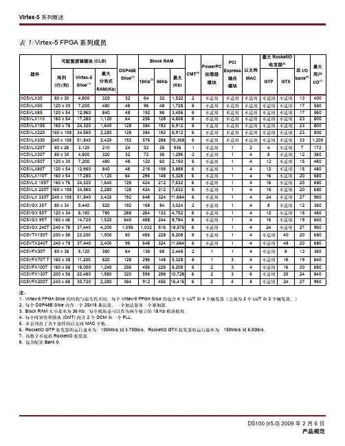
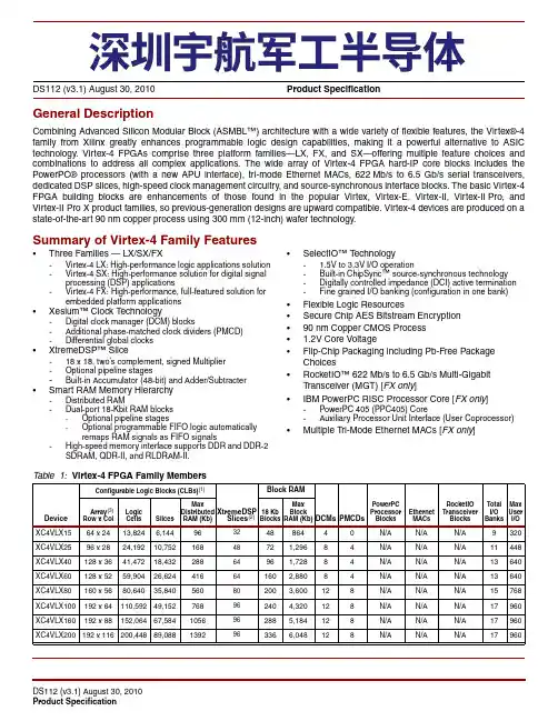
DS100 (v5.1) August 21, 2015Product Specification General DescriptionUsing the second generation ASMBL™ (Advanced Silicon Modular Block) column-based architecture, the Virtex-5 family contains five distinct platforms (sub-families), the most choice offered by any FPGA family. Each platform contains a different ratio of features to address the needs of a wide variety of advanced logic designs. In addition to the most advanced, high-performance logic fabric, Virtex-5FPGAs contain many hard-IP system level blocks, including powerful 36-Kbit block RAM/FIFOs, second generation 25x18 DSP slices, SelectIO™ technology with built-in digitally-controlled impedance, ChipSync™ source-synchronous interface blocks, system monitor functionality, enhanced clock management tiles with integrated DCM (Digital Clock Managers) and phase-locked-loop (PLL) clock generators, and advanced configuration options. Additional platform dependant features include power-optimized high-speed serial transceiver blocks for enhanced serial connectivity, PCI Express® compliant integrated Endpoint blocks, tri-mode Ethernet MACs (Media Access Controllers), and high-performance PowerPC®440 microprocessor embedded blocks. These features allow advanced logic designers to build the highest levels of performance and functionality into their FPGA-based systems. Built on a 65-nm state-of-the-art copper process technology, Virtex-5 FPGAs are a programmable alternative to custom ASIC technology. Most advanced system designs require the programmable strength of FPGAs. Virtex-5 FPGAs offer the best solution for addressing the needs of high-performance logic designers, high-performance DSP designers, and high-performance embedded systems designers with unprecedented logic, DSP, hard/soft microprocessor, and connectivity capabilities. The Virtex-5 LXT, SXT, TXT, and FXT platforms include advanced high-speed serial connectivity and link/transaction layer capability.Summary of Virtex-5 FPGA FeaturesVirtex-5 Family OverviewSystem Blocks Specific to the LXT, SXT, TXT, and FXT DevicesIntegrated Endpoint Block for PCI Express Compliance•Works in conjunction with RocketIO GTP transceivers (LXT and SXT) and GTX transceivers (TXT and FXT) to deliver full PCI Express Endpoint functionality withminimal FPGA logic utilization.•Compliant with the PCI Express Base Specification 1.1•PCI Express Endpoint block or Legacy PCI Express Endpoint block•x8, x4, or x1 lane width•Power management support•Block RAMs used for buffering•Fully buffered transmit and receive •Management interface to access PCI Express configuration space and internal configuration •Supports the full range of maximum payload sizes •Up to 6x32 bit or 3x64 bit BARs (or a combination of32 bit and 64 bit)Tri-Mode Ethernet Media Access Controller •Designed to the IEEE 802.3-2002 specification •Operates at 10, 100, and 1,000 Mb/s•Supports tri-mode auto-negotiation•Receive address filter (5 address entries)•Fully monolithic 1000Base-X solution with RocketIO GTP transceivers•Supports multiple external PHY connections (RGMII, GMII, etc.) interfaces through soft logic and SelectIOresources•Supports connection to external PHY device through SGMII using soft logic and RocketIO GTP transceivers •Receive and transmit statistics available through separate interface•Separate host and client interfaces•Support for jumbo frames•Support for VLAN•Flexible, user-configurable host interface•Supports IEEE 802.3ah-2004 unidirectional modeVirtex-5 Family OverviewRocketIO GTP Transceivers (LXT/SXT only)•Full-duplex serial transceiver capable of 100Mb/s to3.75Gb/s baud rates•8B/10B, user-defined FPGA logic, or no encoding options•Channel bonding support•CRC generation and checking •Programmable pre-emphasis or pre-equalization for the transmitter•Programmable termination and voltage swing •Programmable equalization for the receiver •Receiver signal detect and loss of signal indicator •User dynamic reconfiguration using secondary configuration bus•Out of Band (OOB) support for Serial AT A (SAT A)•Electrical idle, beaconing, receiver detection, and PCI Express and SATA spread-spectrum clocking support •Less than 100mW typical power consumption •Built-in PRBS Generators and Checkers RocketIO GTX Transceivers (TXT/FXT only)•Full-duplex serial transceiver capable of 150Mb/s to6.5Gb/s baud rates•8B/10B encoding and programmable gearbox to support 64B/66B and 64B/67B encoding, user-defined FPGA logic, or no encoding options•Channel bonding support•CRC generation and checking •Programmable pre-emphasis or pre-equalization for the transmitter•Programmable termination and voltage swing •Programmable continuous time equalization for the receiver•Programmable decision feedback equalization for the receiver•Receiver signal detect and loss of signal indicator •User dynamic reconfiguration using secondary configuration bus•OOB support (SAT A)•Electrical idle, beaconing, receiver detection, and PCI Express spread-spectrum clocking support •Low-power operation at all line rates PowerPC 440 RISC Cores (FXT only)•Embedded PowerPC 440 (PPC440) cores−Up to 550MHz operation−Greater than 1000 DMIPS per core−Seven-stage pipeline−Multiple instructions per cycle−Out-of-order execution−32Kbyte, 64-way set associative level 1 instruction cache−32Kbyte, 64-way set associative level 1 data cache−Book E compliant•Integrated crossbar for enhanced system performance −128-bit Processor Local Buses (PLBs)−Integrated scatter/gather DMA controllers−Dedicated interface for connection to DDR2 memory controller−Auto-synchronization for non-integer PLB-to-CPU clock ratios•Auxiliary Processor Unit (APU) Interface and Controller −Direct connection from PPC440 embedded block to FPGA fabric-based coprocessors−128-bit wide pipelined APU Load/Store−Support of autonomous instructions: no pipeline stalls−Programmable decode for custom instructionsArchitectural DescriptionVirtex-5 FPGA Array OverviewVirtex-5 devices are user-programmable gate arrays with various configurable elements and embedded cores optimized for high-density and high-performance system designs. Virtex-5 devices implement the following functionality:Global ClockingThe CMTs and global-clock multiplexer buffers provide a complete solution for designing high-speed clock networks. Each CMT contains two DCMs and one PLL. The DCMs and PLLs can be used independently or extensively cascaded. Up to six CMT blocks are available, providing up to eighteen total clock generator elements.Each DCM provides familiar clock generation capability. To generate deskewed internal or external clocks, each DCM can be used to eliminate clock distribution delay. The DCM also provides 90°, 180°, and 270° phase-shifted versions of the output clocks. Fine-grained phase shifting offers higher-resolution phase adjustment with fraction of the clock period increments. Flexible frequency synthesis provides a clock output frequency equal to a fractional or integer multiple of the input clock frequency.To augment the DCM capability, Virtex-5 FPGA CMTs also contain a PLL. This block provides reference clock jitter filtering and further frequency synthesis options.Virtex-5 devices have 32 global-clock MUX buffers. The clock tree is designed to be differential. Differential clocking helps reduce jitter and duty cycle distortion.DSP48E SlicesDSP48E slice resources contain a 25x18 two’s complement multiplier and a 48-bitadder/subtacter/accumulator. Each DSP48E slice also contains extensive cascade capability to efficiently implement high-speed DSP algorithms.The Virtex-5 FPGA DSP48E slice features are further discussed in Virtex-5 FPGA XtremeDSP Design Considerations.Routing ResourcesAll components in Virtex-5 devices use the same interconnect scheme and the same access to the global routing matrix. In addition, the CLB-to-CLB routing is designed to offer a complete set of connectivity in as few hops as possible. Timing models are shared, greatly improving the predictability of the performance for high-speed designs.Boundary ScanBoundary-Scan instructions and associated data registers support a standard methodology for accessing and configuring Virtex-5 devices, complying with IEEE standards1149.1 and 1532.ConfigurationVirtex-5 devices are configured by loading the bitstream into internal configuration memory using one of the following modes:•Slave-serial mode•Master-serial mode•Slave SelectMAP mode•Master SelectMAP mode•Boundary-Scan mode (IEEE-1532 and -1149)•SPI mode (Serial Peripheral Interface standard Flash)•BPI-up/BPI-down modes (Byte-wide Peripheral interface standard x8 or x16 NOR Flash)In addition, Virtex-5 devices also support the following configuration options:•256-bit AES bitstream decryption for IP protection •Multi-bitstream management (MBM) for cold/warm boot support•Parallel configuration bus width auto-detection •Parallel daisy chain•Configuration CRC and ECC support for the most robust, flexible device integrity checkingVirtex-5 device configuration is further discussed in the Virtex-5 FPGA Configuration Guide.System MonitorFPGAs are an important building block in highavailability/reliability infrastructure. Therefore, there is need to better monitor the on-chip physical environment of the FPGA and its immediate surroundings within the system. For the first time, the Virtex-5 family System Monitor facilitates easier monitoring of the FPGA and its external environment. Every member of the Virtex-5 family contains a System Monitor block. The System Monitor is built around a 10-bit 200kSPS ADC (Analog-to-Digital Converter). This ADC is used to digitize a number of on-chip sensors to provide information about the physical environment within the FPGA. On-chip sensors include a temperature sensor and power supply sensors. Access to the external environment is provided via a number of external analog input channels. These analog inputs are general purpose and can be used to digitize a wide variety of voltage signal types. Support for unipolar, bipolar, and true differential input schemes is provided. There is full access to the on-chip sensors and external channels via the JTAG T AP, allowing the existing JT AG infrastructure on the PC board to be used for analog test and advanced diagnostics during development or after deployment in the field. The System Monitor is fully operational after power up and before configuration of the FPGA. System Monitor does not require an explicit instantiation in a design to gain access to its basic functionality. This allows the System Monitor to be used even at a late stage in the design cycle.The Virtex-5 FPGA System Monitor is further discussed in the Virtex-5 FPGA System Monitor User Guide.。
Revision HistoryThe following table shows the revision history for this document.Date Version Revision03/31/08 1.0Initial Xilinx release.05/08/08 1.1•Table5-3: Corrected PCI Express Rev 2 parameter values.•Table7-14: Corrected OOB Nominal Threshold Voltage sub-table forOOBDETECT_THRESHOLD_0/1•Table7-35 and Table7-37: Corrected RXBUFSTATUS0/1 description.•Table E-1 and Table E-2: Replaced with new tables.09/04/08 1.2•Added 3G-SDI to Table1-1 and Table5-3.•Added (Pad) to all pins in Table1-2.•Revised DIV = 5 and DIV = 4 bulleted conditions under Equation5-1.•Revised descriptions of DFEEYEDACMONITOR0/1, DFETAP20/1,DFETAP2MONITOR0/1, DFETAP30/1, DFETAP3MONITOR0/1, DFETAP40/1, andDFETAP4MONITOR0/1 in Table7-5.•Revised descriptions of DFE_CAL_TIME, DFE_CFG_0/1, andRX_EN_IDLE_HOLD_DFE_0/1 in Table7-6.•Added “Channel BER Optimization Approach”, “Use Mode – Fixed Tap Mode”,“Example RX Linear Equalizer and DFE Settings for Chip-to-Chip Applications”, and“Example RX Linear Equalizer and DFE Settings for Backplane Applications” to“Decision Feedback Equalization” in Chapter7.•Corrected the 101 and 110 encodings for RXSTATUS0/1 in Table7-13.•Revised the second sentence in the Overview section of “Configurable ChannelBonding (Lane Deskew)” in Chapter7.•Added note about channel-bonded GTX transceivers being in the same column onpage227 and in Figure7-34.•Added nominal rating to RREF in footnote 3 of Table10-2 and in the note followingthe table.•Added Boundary-Scan footnote to page267.•Revised “Special Conditions: Unused GTX_DUAL Column” in Chapter10.•Added notes about BGA adjacency guidelines to “SelectIO to GTX CrosstalkGuidelines” in Chapter10.UG198 (v3.0) October 30, 2009RocketIO GTX Transceiver User GuideRocketIO GTX Transceiver User Guide UG198 (v3.0) October 30, 2009Chapter 10:GTX-to-Board InterfaceTable 10-10 shows the configuration for Use Case 5, where:•A GTX_DUAL tile is used only for forwarding resistor calibration information generated in the center tile of the column and for forwarding a reference clock •Both transceivers are unused •Boundary-Scan is always functional MGTAVTTRX GND-MGTAVTTRXC MGTAVTTRX (1)Y MGTAVCCPLL GND-MGTAVCC V CCINT-MGTRREF MGTAVTTTX with resistor (2)-Notes:1.Connect to MGTAVTTRX of a used GTX_DUAL tile. Refer to Figure 10-3, page 257.2.Connect to MGTAVTTTX of a used GTX_DUAL tile. Refer to Figure 10-1, page 256 and Figure 10-4,page 258.Table 10-10:Use Case 5Pin or Pin Pair Connect ToFilter MGTRXP/MGTRXN GND-MGTTXP/MGTTXN Floating, no connection-MGTREFCLKP/MGTREFCLKN Floating, no connection-MGTAVTTTX 1.2V dedicated supply (1)Y MGTAVTTRX GND-MGTAVTTRXC MGTAVTTRX (2)Y MGTAVCCPLL GND-MGTAVCC V CCINT-MGTRREFMGTAVTTTX with resistor (3)-Notes:1.Refer to Figure 10-5, page 262.2.Connect to MGTAVTTRX of a used GTX_DUAL tile. Refer to Figure 10-3, page 257.3.Connect to MGTAVTTTX of a used GTX_DUAL tile. Refer to Figure 10-1, page 256 and Figure 10-4,page 258.Table 10-9:Use Case 4 (Cont’d)Pin or Pin Pair Connect ToFilterRocketIO GTX Transceiver User Guide UG198 (v3.0) October 30, 2009Chapter 6:GTX Transmitter (TX)。
SelectIO™ DC Input and Output LevelsValues for V IL and V IH are recommended input voltages. Values for I OL and I OH are guaranteed over the recommended operating conditions at the V OL and V OH test points. Only selected standards are tested. These are chosen to ensure that all standards meet their specifications. The selected standards are tested at a minimum V CCO with the respective V OL and V OH voltage levels shown. Other standards are sample tested.Table 7:SelectIO DC Input and Output LevelsI/O StandardV IL V IH V OL V OH I OL I OH V, Min V, Max V, Min V, Max V, Max V, Min mA mALVTTL–0.30.8 2.0 3.450.4 2.4Note(3)Note(3) LVCMOS33,LVDCI33–0.30.8 2.0 3.450.4V CCO–0.4Note(3)Note(3)LVCMOS25,LVDCI25–0.30.7 1.7V CCO+0.30.4V CCO–0.4Note(3)Note(3)LVCMOS18,LVDCI18–0.335% V CCO65% V CCO V CCO+0.30.45V CCO–0.45Note(4)Note(4)LVCMOS15,LVDCI15–0.335% V CCO65% V CCO V CCO+0.325%V CCO75%V CCO Note(4)Note(4) LVCMOS12–0.335% V CCO65% V CCO V CCO+0.325%V CCO75%V CCO Note(6)Note(6) PCI33_3(5)–0.230% V CCO50% V CCO V CCO10%V CCO90%V CCO Note(5)Note(5) PCI66_3(5)–0.230% V CCO50% V CCO V CCO10%V CCO90%V CCO Note(5)Note(5) PCI-X(5)–0.235% V CCO50% V CCO V CCO10%V CCO90%V CCO Note(5)Note(5) GTLP–0.3V REF–0.1V REF+0.1–0.6N/A36N/A GTL–0.3V REF–0.05V REF+0.05–0.4N/A32N/A HSTL I_12–0.3V REF–0.1V REF+0.1V CCO+0.325%V CCO75%V CCO 6.3 6.3 HSTL I(2)–0.3V REF–0.1V REF+0.1V CCO+0.30.4V CCO–0.48–8 HSTL II(2)–0.3V REF–0.1V REF+0.1V CCO+0.30.4V CCO–0.416–16 HSTL III(2)–0.3V REF–0.1V REF+0.1V CCO+0.30.4V CCO–0.424–8 HSTL IV(2)–0.3V REF–0.1V REF+0.1V CCO+0.30.4V CCO–0.448–8 DIFF HSTL I(2)–0.350% V CCO–0.150% V CCO+0.1V CCO+0.3––––DIFF HSTL II(2)–0.350% V CCO–0.150% V CCO+0.1V CCO+0.3––––SSTL2I–0.3V REF–0.15V REF+0.15V CCO+0.3V TT–0.61V TT+0.618.1–8.1 SSTL2II–0.3V REF–0.15V REF+0.15V CCO+0.3V TT–0.81V TT+0.8116.2–16.2DIFF SSTL2I–0.350% V CCO–0.1550%V CCO+0.15V CCO+0.3––––DIFF SSTL2II–0.350% V CCO–0.1550%V CCO+0.15V CCO+0.3––––SSTL18I–0.3V REF–0.125V REF+0.125V CCO+0.3V TT–0.47V TT+0.47 6.7–6.7 SSTL18II–0.3V REF–0.125V REF+0.125V CCO+0.3V TT–0.60V TT+0.6013.4–13.4DIFF SSTL18I–0.350% V CCO–0.12550%V CCO+0.125V CCO+0.3––––DIFF SSTL18II–0.350% V CCO–0.12550%V CCO+0.125V CCO+0.3––––Notes:1.Tested according to relevant specifications.2.Applies to both 1.5V and 1.8V HSTL.ing drive strengths of 2, 4, 6, 8, 12, 16, or 24mA.ing drive strengths of 2, 4, 6, 8, 12, or 16mA.5.For more information on PCI33_3, PCI66_3, and PCI-X, refer to UG190: Virtex-5 FPGA User Guide, Chapter 6, 3.3V I/O Design Guidelines.6.Supported drive strengths of 2, 4, 6, or 8mA.Symbol DC Parameter Conditions Min Typ Max Units V CCO Supply Voltage 2.38 2.5 2.63V V OD Differential Output Voltage R T = 100Ω across Q and Q signals495600715mV ΔV OD Change in V OD Magnitude–1515mV V OCM Output Common Mode Voltage R T = 100Ω across Q and Q signals495600715mV ΔV OCM Change in V OCM Magnitude–1515mV V ID Input Differential Voltage2006001000mV ΔV ID Change in V ID Magnitude–1515mV V ICM Input Common Mode Voltage440600780mV ΔV ICM Change in V ICM Magnitude–1515mVTable 27:GTP_DUAL Tile Quiescent Supply CurrentSymbol Description Typ(1)Max UnitsI AVTTTXQ Quiescent MGTAVTTTX (transmitter termination) supply current8.518mAI AVCCPLLQ Quiescent MGTAVCCPLL (PLL) supply current818mAI AVTTRXQ Quiescent MGTAVTTRX (receiver termination) supply current. Includes0.10.8mAMGTAVTTRXCQ.I AVCCQ Quiescent MGTAVCC (analog) supply current 2.511mA Notes:1.Typical values are specified at nominal voltage, 25°C.2.Device powered and unconfigured.3.Currents for conditions other than values specified in this table can be obtained by using the XPOWER Estimator (XPE) or XPOWERAnalyzer (XPA) tools.4.GTP_DUAL tile quiescent supply current for an entire device can be calculated by multiplying the values in this table by the number ofavailable GTP_DUAL tiles in the target LXT or SXT device.GTX_DUAL Tile Switching CharacteristicsConsult UG198:Virtex-5 FPGA RocketIO GTX Transceiver User Guide for further information.Table 42:GTX_DUAL Tile PerformanceSymbol DescriptionSpeed Grade Units -3-2-1F GTXMAX Maximum GTX transceiver data rate 6.5 6.5 4.25Gb/s F GPLLMAX Maximum PLL frequency 3.25 3.25 3.25GHz F GPLLMINMinimum PLL frequency1.481.481.48GHzTable 43:Dynamic Reconfiguration Port (DRP) in the GTX_DUAL Tile Switching CharacteristicsSymbol DescriptionSpeed Grade Units -3-2-1F GTXDRPCLKGTX DCLK (DRP clock) maximum frequency200175150MHzTable 44:GTX_DUAL Tile Reference Clock Switching CharacteristicsSymbol DescriptionConditionsAll Speed Grades Units Min Typ Max F GCLK Reference clock frequency range (1)CLK60650MHz T RCLK Reference clock rise time 20%–80%200ps T FCLK Reference clock fall time 80%–20%200ps T DCREF Reference clock duty cycle CLK 405060%T GJTT Reference clock total jitter (2, 3)At 100KHz –145dBc/Hz At 1MHz –150dBc/Hz T LOCK Clock recovery frequency acquisition timeInitial PLL lock0.251ms T PHASE Clock recovery phase acquisition timeLock to data after PLL has locked to the reference clock200µsNotes:1.GREFCLK can be used for serial bit rates up to 1Gb/s; however, Jitter Specifications are not guaranteed when using GREFCLK.2.GTX_DUAL jitter characteristics measured using a clock with specification T GJTT . A reference clock with higher phase noise can be used with link margin trade off.3.The selection of the reference clock is application dependent. This parameter describes the quality of the reference clock used during transceiver jitter characterization - see Table 46 and Table 47.Figure 10:Reference Clock Timing Parameters。
Chapter 4:LPDDR2 SDRAM Memory Interface Solution overall electrical propagation delay. Different die in the same package might have different delays for the same package pin. If this is expected, the values should be averaged appropriately to decrease the maximum possible performance for the target device. These rules indicate the maximum electrical delays between LPDDR2 SDRAM signals:•The maximum electrical delay between any DQ or DM and its associated DQS/DQS# must be ≤ ±15ps.•The maximum electrical delay between any address and control signals and the corresponding CK/CK# must be ≤ ±25ps, with 15 ps being the optimum target.•The maximum electrical delay between any DQS/DQS# and CK/CK# must be < ±25 ps. ClockingThe 7 series FPGA MIG LPDDR2 SDRAM design has two clock inputs, the reference clock and the system clock. The reference clock drives the IODELAYCTRL components in the design, while the system clock input is used to create all MIG design clocks that are used to clock the internal logic, the frequency reference clocks to the phasers, and a synchronization pulse required for keeping PHY control blocks synchronized in multi-I/O bank implementations. For more information on clocking architecture, see Clocking Architecture, page585.The MIG tool allows you to input the Memory Clock Period and then lists available Input Clock Periods that follow the supported clocking guidelines. Based on these two clock periods selections, the generated MIG core appropriately sets the MMCM parameters. The MIG tool enables automatic generation of all supported clocking structures. For information on how to use the MIG tool to set up the desired clocking structure including input clock placement, input clock frequency, and IDELAYCTRL ref_clk generation, see Creating 7 Series FPGA LPDDR2 SDRAM Memory Controller Block Design, page529.Input Clock Guidelines•MMCM Guidelines°CLKFBOUT_MULT_F (M) must be between 1 and 16 inclusive.°DIVCLK_DIVIDE (D, Input Divider) can be any value supported by the MMCME2 parameter.°CLKOUT_DIVIDE (O, Output Divider) must be 2 for 400 MHz and up operation and 4 for below 400 MHz operation.For QDR II+ SRAM interfaces that have the memory system input clock(sys_clk_p/sys_clk_n) placed on CCIO pins within one of the memory banks, MIG assigns the DIFF_HSTL_I I/O standard (VCCO = 1.5V) to the CCIO pins. Because the same differential input receiver is used for both DIFF_HSTL_I and LVDS inputs, an LVDS clock source can be connected directly to the DIFF_HSTL_I CCIO pins. For more details on usage and required circuitry for LVDS and LVDS_25 I/O Standards, see the 7Series FPGAs SelectIO™ Resources User Guide (UG471) [Ref2].TerminationThese recommendations apply to termination for QDR II+ SRAM:•Simulation (using IBIS or other) is highly recommended. The loading of command and address signals depends on various factors, such as speed requirements andtermination topology. Loading can be a limiting factor in reaching a performancetarget.•Command and Address signals should be terminated to V TT through a 50Ω resistor.•Write Clock (K_P/N) does not require an external termination if ODT is available. If ODT is not available, each line should be terminated to V TT through a 50Ω resistor.•Write Data lines (D) do not require an external termination if ODT is available. If ODT is not available, each line should be terminated to V TT through a 50Ω resistor.•Read Clock (CQ) does not require an external termination and should use DCI. Set the DCI termination for each single-ended line to 50Ω.•Read Data lines (Q, QVLD) do not require an external termination and should use DCI.Set the DCI termination to 50Ω.I/O StandardsThe MIG tool generates the appropriate XDC for the core with SelectIO™ interface standards based on the type of input or output to the 7series FPGAs. These standards should not be changed. Table2-14 contains a list of the ports together with the I/O standard used.Table 2-14:I/O StandardsSignal(1)Direction I/O Standardqdr_bw_n Output HSTL_Iqdr_cq_p, qdr_cq_n Input HSTL_I_DCIqdr_d Output HSTL_Iqdr_k_p, qdr_k_n InOut DIFF_HSTL_IIqdr_q Input HSTL_I_DCIqdr_r_n Output HSTL_I。
IntroductionThe Spartan®-3 family of Field-Programmable Gate Arrays is specifically designed to meet the needs of high volume, cost-sensitive consumer electronic applications. Theeight-member family offers densities ranging from 50,000 to 5,000,000 system gates, as shown in Table 1.The Spartan-3 family builds on the success of the earlier Spartan-IIE family by increasing the amount of logicresources, the capacity of internal RAM, the total number of I/Os, and the overall level of performance as well as by improving clock management functions. Numerous enhancements derive from the Virtex®-II platform technology. These Spartan-3 FPGA enhancements,combined with advanced process technology, deliver more functionality and bandwidth per dollar than was previously possible, setting new standards in the programmable logic industry.Because of their exceptionally low cost, Spartan-3 FPGAs are ideally suited to a wide range of consumer electronics applications, including broadband access, home networking, display/projection and digital television equipment.The Spartan-3 family is a superior alternative to mask programmed ASICs. FPGAs avoid the high initial cost, the lengthy development cycles, and the inherent inflexibility of conventional ASICs. Also, FPGA programmability permits design upgrades in the field with no hardware replacement necessary, an impossibility with ASICs.Features•Low-cost, high-performance logic solution for high-volume,consumer-oriented applications •Densities up to 74,880 logic cells •SelectIO™ interface signaling •Up to 633 I/O pins •622+ Mb/s data transfer rate per I/O •18 single-ended signal standards •8 differential I/O standards including LVDS, RSDS •Termination by Digitally Controlled Impedance •Signal swing ranging from 1.14V to 3.465V •Double Data Rate (DDR) support •DDR, DDR2 SDRAM support up to 333Mb/s •Logic resources •Abundant logic cells with shift register capability •Wide, fast multiplexers •Fast look-ahead carry logic •Dedicated 18 x 18 multipliers •JT AG logic compatible with IEEE 1149.1/1532•SelectRAM™ hierarchical memory •Up to 1,872 Kbits of total block RAM •Up to 520 Kbits of total distributed RAM •Digital Clock Manager (up to four DCMs)•Clock skew elimination •Frequency synthesis •High resolution phase shifting•Eight global clock lines and abundant routing•Fully supported by Xilinx ISE ® and WebP ACK ™ software development systems•MicroBlaze ™ and PicoBlaze ™ processor, PCI ®,PCI Express® PIPE Endpoint , and other IP cores •Pb-free packaging options•Automotive Spartan-3 XA Family variantDS099 (v3.1) June 27, 2013Product SpecificationTable 1:Summary of Spartan-3 FPGA AttributesDeviceSystem Gates EquivalentLogic Cells (1)CLB Array(One CLB = Four Slices)Distributed RAM Bits (K=1024)BlockRAM Bits (K=1024)DedicatedMultipliersDCMsMax.User I/OMaximumDifferentialI/O Pairs Rows ColumnsTotalCLBs XC3S50(2)50K 1,728161219212K 72K 4212456XC3S200(2)200K 4,320242048030K 216K 12417376XC3S400(2)400K 8,064322889656K 288K 164264116XC3S1000(2)1M 17,28048401,920120K 432K 244391175XC3S1500 1.5M 29,95264523,328208K 576K 324487221XC3S20002M 46,08080645,120320K 720K 404565270XC3S40004M 62,20896726,912432K 1,728K 964633300XC3S50005M74,880104808,320520K1,872K1044633300Notes:1.Logic Cell = 4-input Look-Up T able (LUT) plus a ‘D’ flip-flop. "Equivalent Logic Cells" equals "T otal CLBs" x 8 Logic Cells/CLB x 1.125 effectiveness.2.These devices are available in Xilinx Automotive versions as described in DS314: Spartan-3 Automotive XA FPGA Family .Revision HistoryTable 4:Example Ordering InformationDeviceSpeed GradePackage Type/Number of PinsTemperature Range (T j )XC3S50-4Standard Performance VQ(G)100100-pin Very Thin Quad Flat Pack (VQFP)C Commercial (0°C to 85°C)XC3S200-5High Performance (1)CP(G)132(2)132-pin Chip-Scale Package (CSP)IIndustrial (–40°C to 100°C)XC3S400TQ(G)144144-pin Thin Quad Flat Pack (TQFP)XC3S1000PQ(G)208208-pin Plastic Quad Flat Pack (PQFP)XC3S1500FT(G)256256-ball Fine-Pitch Thin Ball Grid Array (FTBGA)XC3S2000FG(G)320320-ball Fine-Pitch Ball Grid Array (FBGA)XC3S4000FG(G)456456-ball Fine-Pitch Ball Grid Array (FBGA)XC3S5000FG(G)676676-ball Fine-Pitch Ball Grid Array (FBGA)FG(G)900900-ball Fine-Pitch Ball Grid Array (FBGA)FG(G)1156(2)1156-ball Fine-Pitch Ball Grid Array (FBGA)Notes:Date Version Description04/11/2003 1.0Initial Xilinx release.04/24/2003 1.1Updated block RAM, DCM, and multiplier counts for the XC3S50.12/24/2003 1.2Added the FG320 package.07/13/2004 1.3Added information on Pb-free packaging options.01/17/20051.4Referenced Spartan-3 XA Automotive FPGA families in Table 1. Added XC3S50CP132,XC3S2000FG456, XC3S4000FG676 options to T able 3. Updated Package Marking to show mask revision code, fabrication facility code, and process technology code.08/19/2005 1.5Added package markings for BGA packages (Figure 3) and CP132/CPG132 packages (Figure 4). Added differential (complementary single-ended) HSTL and SSTL I/O standards.04/03/2006 2.0Increased number of supported single-ended and differential I/O standards.04/26/2006 2.1Updated document links.05/25/2007 2.2Updated Package Marking to allow for dual-marking.11/30/2007 2.3Added XC3S5000 FG(G)676 to Table 3. Noted that FG(G)1156 package is being discontinued and updated max I/O count.06/25/2008 2.4Updated max I/O counts based on FG1156 discontinuation. Clarified dual mark in Package Marking . Updated formatting and links.12/04/2009 2.5CP132 and CPG132 packages are being discontinued. Added link to Spartan-3 FPGA customer notices. Updated Table 3 with package footprint dimensions.10/29/20123.0Added Notice of Disclaimer section. Per XCN07022, updated the discontinued FG1156 and FGG1156 package discussion throughout document. Per XCN08011, updated the discontinued CP132 and CPG132 package discussion throughout document. Although the package is discontinued, updated the marking on Figure 4. This product is not recommended for new designs.06/27/2013 3.1Removed banner. This product IS recommended for new designs.Figure 7:Simplified IOB DiagramAccording to Figure 7, the clock line OTCLK1 connects the CK inputs of the upper registers on the output and three-state paths. Similarly, OTCLK2 connects the CK inputs for the lower registers on the output and three-state paths. The upper and lower registers on the input path have independent clock lines: ICLK1 and ICLK2. The enable line OCE connects the CE inputs of the upper and lower registers on the output path. Similarly, TCE connects the CE inputs for the register pair on the three-state path and ICE does the same for the register pair on the input path. The Set/Reset (SR) line entering the IOB is common to all six registers, as is the Reverse (REV) line.Each storage element supports numerous options in addition to the control over signal polarity described in the IOB Overview section. These are described in Table 6.Double-Data-Rate TransmissionDouble-Data-Rate (DDR) transmission describes the technique of synchronizing signals to both the rising and falling edges of the clock signal. Spartan-3 devices use register-pairs in all three IOB paths to perform DDR operations.The pair of storage elements on the IOB’s Output path (OFF1 and OFF2), used as registers, combine with a special multiplexer to form a DDR D-type flip-flop (FDDR). This primitive permits DDR transmission where output data bits are synchronized to both the rising and falling edges of a clock. It is possible to access this function by placing either an FDDRRSE or an FDDRCPE component or symbol into the design. DDR operation requires two clock signals (50% duty cycle), one the inverted form of the other. These signals trigger the two registers in alternating fashion, as shown in Figure 8. Commonly, the Digital Clock Manager (DCM) generates the two clock signals by mirroring an incoming signal, then shifting it 180 degrees. This approach ensures minimal skew between the two signals.The storage-element-pair on the Three-State path (TFF1 and TFF2) can also be combined with a local multiplexer to form an FDDR primitive. This permits synchronizing the output enable to both the rising and falling edges of a clock. This DDR operation is realized in the same way as for the output path.The storage-element-pair on the input path (IFF1 and IFF2) allows an I/O to receive a DDR signal. An incoming DDR clock signal triggers one register and the inverted clock signal triggers the other register. In this way, the registers take turns capturing bits of the incoming DDR data signal.Table 6:Storage Element OptionsOption Switch FunctionSpecificityFF/Latch Chooses between an edge-sensitive flip-flop or a level-sensitive latchIndependent for each storage element.SYNC/ASYNC Determines whether SR is synchronous or asynchronousIndependent for each storage element.SRHIGH/SRLOWDetermines whether SR acts as a Set, which forces the storage element to a logic “1" (SRHIGH) or a Reset, which forces a logic “0” (SRLOW).Independent for each storage element, except when using FDDR. In the latter case, the selection for the upper element (OFF1 or TFF2) applies to both elements.INIT1/INIT0In the event of a Global Set/Reset, after configuration or upon activation of the GSR net, this switch decides whether to set or reset a storage element. By default, choosing SRLOW also selects INIT0; choosing SRHIGH also selects INIT1.Independent for each storage element, except when using FDDR. In the latter case, selecting INIT0 for one element applies to both elements (even though INIT1 is selected for the other).。
Thermal SpecificationsSummaryThis chapter provides thermal data associated with Virtex®-5 FPGA packages. Thefollowing topics are discussed:•Introduction•Power Management Strategy•Some Thermal Management Options•Support for Compact Thermal Models (CTM)•ReferencesIntroductionVirtex-5 devices are offered exclusively in thermally efficient flip-chip BGA packages.These 1.0 mm flip-chip packages range in pin-count from the smaller 19x19mm FF324 tothe 42.5x42.5mm FF1760. The suite of packages is used to address the various powerrequirements of the Virtex-5devices. All Virtex-5 devices are implemented in the 65nmprocess technologySimilar to Virtex-4 FPGAs, all Virtex-5 devices feature versatile SelectIO™ resources thatsupport a variety of I/O standards. They also include Digital Clock Managers (DCMs),DSPs, and other traditional features and blocks (such as block RAM) contained in earlierVirtex products.In line with Moore's law, the transistor count in this family of devices has been increasedsubstantially. Though several innovative features at the silicon level have been deployed tominimize power dissipation, including leakage at the 65nm node, these products havemore densely packed transistors and embedded blocks with the capability to run fasterthan before. Thus, a fully configured Virtex-5 design that exploits the fabric speed andincorporates several embedded circuits and systems can present power consumptionchallenges that must be managed.Unlike features in an ASIC or a microprocessor, the combination of FPGA features used inan user application are not known to the component supplier. Therefore, it remains achallenge for Xilinx to predict the power requirements of a given FPGA when it leaves thefactory. Accurate estimates are obtained when the board design takes shape. For thispurpose, Xilinx offers and supports a suite of integrated device power analysis tools tohelp users quickly and accurately estimate their design power requirements. Virtex-5devices are supported similarly to previous FPGA products. The uncertainty of designpower requirements makes it difficult to apply canned thermal solutions to fit all users.Therefore, Xilinx devices do not come with preset thermal solutions. The user’s operatingconditions dictate the appropriate solution.Power Management Strategy•Heat Sinking Solutions at the System LevelDepending on the system's physical as well as mechanical constraints, the expectation is that the thermal budget is maintained with custom or OEM heat sink solutions,providing the third prong in the thermal management strategy. At this point, Xilinx has left the heat sink solution to the system-level designers who can tailor the design and solution to the constraints of their systems, being fully aware that the part has certain inherent capabilities for delivering the heat to the surface.Heat sink solutions do exist and can be effective on these low θJB flip-chip platforms.Table 6-3 below illustrates a finned heat sink solution matrix in Network environment (1U and 2U) arrangement for 35mm packages and up for power ranging from 15W to 40W. The AAVID standard finned heat sink offerings are used to illustrate the coverage given thermal budgets of ΔT =35°C and ΔT =45°C scenarios. Other heat sink configurations can be explored similarly.The Virtex-5 FPGA packages can be grouped into medium- and high-performancepackages based on their power handling capabilities. All Virtex-5 FPGA packages can use thermal enhancements, ranging from simple airflow to schemes that can include passive as well as active heat sinks. This is particularly true for the bigger flip-chip BGA packages where system designers have the option to further enhance the packages with bigger and more elaborate heat sinks to handle excesses of 25W with arrangements that consider system –physical constraints as illustrated in Table 6-3.Table 6-3:Finned Heat Sink Solution Matrix for Large Flip-chip BGA in Network Package Power(W)35 x 35 mmFF1136/FF1153/FF115642.5 x 42.5 mmFF1738/FF1759/FF1760ΔT=35°CΔT=45°CΔT=35°CΔT=45°C15W1U (5)Note 1Note 12U (6)Note 1Note 125W1U (5)Note 4Note 2Note 4Note 22U (6)Note 2Note 1Note 2Note 135W1U (5)Note 4Note 3Note 4Note 32U (6)Note 4Note 2Note 4Note 240W1U (5)––Note 4Note 32U (6)Note 3Note 2Notes:1.Solution available at 200 LFM, for example, AAVID finned part number 68520, 72390, 72415.2.Solution available at 400 LFM, for example, AAVID finned part number 68520, 69920.3.Solution available at 600 LFM, for example, AAVID finned part number 72390, 69920, 74590.4.No standard. AAVID finned solution below 600 LFM—custom finned might be required.5.For 1U Height—(max heat sink height = 26mm)6.For 2U Height—(max heat sink height = 64mmChapter 6:Thermal SpecificationsThe flip-chip thermal management chart in Figure6-2 illustrates simple but incrementalpower management schemes that can be applied on a flip-chip BGA package.FF665, FFG665, EF665, FFV665 Flip-Chip Fine-PitchBGA Package Specifications (1.00mm Pitch)Figure 4-3: FF665, FFG665, EF665, FFV665 Flip-Chip Fine-Pitch BGA Package SpecificationsEF1738 Flip-Chip Fine-Pitch BGA Package Specifications (1.00mm Pitch)Figure 4-9:EF1738 Flip-Chip Fine-Pitch BGA Package Specifications。
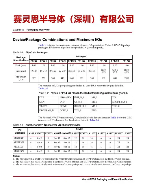
Chapter 1:Packaging OverviewPin DefinitionsTable1-7 lists the pin definitions used in Virtex-5 FPGA packages. Table 1-7:Virtex-5 FPGA Pin DefinitionsPin Name Direction DescriptionUser I/O PinsIO_LXXY_#Input/OutputAll user I/O pins are capable of differential signaling and can implement pairs.Each user I/O is labeled “IO_LXXY_#”, where:IO indicates a user I/O pin.LXXY indicates a differential pair, with XX a unique pair in the bank and Y =[P|N] for the positive/negative sides of the differential pair.Multi-Function PinsIO_LXXY_ZZZ_#Multi-function pins are labelled “IO_LXXY_ZZZ_#”, where ZZZ represents one or more of the following functions in addition to being general purpose user I/O. If not used for their special function, these pins can be user I/O.DnInput In SelectMAP mode, D0 through D31 are configuration data pins. These pins become user I/Os after configuration, unless the SelectMAP port is retained.ADDRnOutput ADDR0–ADDR25 BPI address output. These pins become user I/O after configuration.RSn Output RS0 and RS1 revision select output. FCS_B Output BPI and SPI flash chip select.FOE_B Output BPI flash output enable.FWE_B Output BPI flash write enable.MOSI Output SPI flash data output enable.CSO_B Output Parallel daisy chain chip select. FSn Input FS0–FS2 SPI Flash vendor selection.CCInput These clock pins connect to Clock Capable I/Os. These pins become regular user I/Os when not needed for clocks. If a single-ended clock is connected to the differential CC pair of pins, it must be connected to the positive (P) side of the pair. Clock capable I/Os in the center column can not drive BUFRs.GCInput These clock pins connect to Global Clock Buffers. These pins become regular user I/Os when not needed for clocks. If a single-ended clock is connected to the differential GC pair of pins, it must be connected to the positive (P) side of the pair.SMnP/SMnN Input System Monitor analog inputs.VREFN/A These are input threshold voltage pins. They become user I/Os when an external threshold voltage is not needed (per bank).VRNN/A This pin is for the DCI voltage reference resistor of N transistor (per bank, to be pulled High with reference resistor).VRPN/A This pin is for the DCI voltage reference resistor of P transistor (per bank, to be pulled Low with reference resistor).Pin DefinitionsDedicated Configuration Pins (1)CCLK_0Input/OutputConfiguration clock. Output and input in Master mode or Input in Slave mode.CS_B_0Input In SelectMAP mode, this is the active-low Chip Select signal. D_IN_0Input In bit-serial modes, D_IN is the single-data input.DONE_0Input/OutputDONE is a bidirectional signal with an optional internal pull-up resistor. As an output, this pin indicates completion of the configuration process. As an input, a Low level on DONE can be configured to delay the start-up sequence.D_OUT_BUSY_0OutputIn SelectMAP mode, BUSY controls the rate at which configuration data is loaded.In bit-serial modes, DOUT gives preamble and configuration data to down-stream devices in a daisy chain.Table 1-7:Virtex-5 FPGA Pin Definitions (Continued)Pin NameDirectionDescriptionFF324 Package—LX30 and LX50Table 2-2:FF324 Package—LX30 and LX50 (Continued)Bank Pin Description Pin Number No Connect (NC) 12IO_L8P_CC_12 H612IO_L8N_CC_12(2)H512IO_L9P_CC_12 D212IO_L9N_CC_12(2)C212IO_L10P_CC_12 A112IO_L10N_CC_12(2)A212IO_L11P_CC_12 G412IO_L11N_CC_12(2)F412IO_L12P_VRN_12 C112IO_L12N_VRP_12 B112IO_L13P_12 G312IO_L13N_12 F312IO_L14P_12 F112IO_L14N_VREF_12 E112IO_L15P_12 J512IO_L15N_12 J412IO_L16P_12 H312IO_L16N_12 J312IO_L17P_12 H212IO_L17N_12 J212IO_L18P_12 E212IO_L18N_12 F212IO_L19P_12 G112IO_L19N_12 H113IO_L0P_SM8P_13 K1513IO_L0N_SM8N_13 L1613IO_L1P_SM7P_13 L1713IO_L1N_SM7N_13 K1613IO_L2P_SM6P_13 K1413IO_L2N_SM6N_13 L1413IO_L3P_SM5P_13 M1813IO_L3N_SM5N_13 L1813IO_L4P_13 L1313IO_L4N_VREF_13 M1313IO_L5P_SM4P_13 P1813IO_L5N_SM4N_13 N1813IO_L6P_SM3P_13 M1413IO_L6N_SM3N_13 N1513IO_L7P_SM2P_13P17Table 2-2:FF324 Package—LX30 and LX50 (Continued)Bank Pin DescriptionPin NumberNo Connect (NC)NA MGTAVTTRX_125AM29NA MGTRXN0_125AP29NA MGTAVCCPLL_125AM26NA MGTRXN1_125AP28NA MGTREFCLKN_125AM28NA MGTRXP1_125AP27NA MGTREFCLKP_125AL28NA MGTTXN1_125AN27NA MGTTXP1_125AN26NAMGTTXP0_126AN4Table 2-7:FF1156 Package—TX150T (Continued)Bank Pin DescriptionPin NumberNo Connect (NC)。
Virtex-5 FPGA Electrical CharacteristicsVirtex®-5 FPGAs are available in -3, -2, -1 speed grades, with -3 having the highest performance. Virtex-5 FPGA DC and AC characteristics are specified for both commercial and industrial grades. Except the operating temperature range or unless otherwise noted, all the DC and ACelectrical parameters are the same for a particular speed grade (that is, the timing characteristics of a -1 speed grade industrial device are the same as for a -1 speed grade commercial device). However, only selected speed grades and/or devices might be available in the industrial range.All supply voltage and junction temperature specifications are representative of worst-case conditions. Theparameters included are common to popular designs and typical applications.This Virtex-5 FPGA data sheet, part of an overall set of documentation on the Virtex-5 family of FPGAs, is available on the Xilinx website:•Virtex-5 Family Overview •Virtex-5 FPGA User Guide•Virtex-5 FPGA Configuration Guide•Virtex-5 FPGA XtremeDSP™ Design Considerations •Virtex-5 FPGA Packaging and Pinout Specification•Embedded Processor Block in Virtex-5 FPGAs Reference Guide•Virtex-5 FPGA RocketIO™ GTP Transceiver User Guide •Virtex-5 FPGA RocketIO GTX Transceiver User Guide •Virtex-5 FPGA Embedded Tri-Mode Ethernet MAC User Guide•Virtex-5 FPGA Integrated Endpoint Block User Guide for PCI Express® Designs•Virtex-5 FPGA System Monitor User Guide •Virtex-5 FPGA PCB Designer’s GuideAll specifications are subject to change without notice.Virtex-5 FPGA DC CharacteristicsDS202 (v5.5) June 17, 2016Product SpecificationTable 1:Absolute Maximum RatingsSymbolDescriptionUnits V CCINT Internal supply voltage relative to GND –0.5 to 1.1V V CCAUX Auxiliary supply voltage relative to GND–0.5 to 3.0V V CCO Output drivers supply voltage relative to GND –0.5 to 3.75V V BATT Key memory battery backup supply –0.5 to 4.05V V REFInput reference voltage–0.5 to 3.75V V IN (3)3.3V I/O input voltage relative to GND (4) (user and dedicated I/Os)–0.75 to 4.05V 3.3V I/O input voltage relative to GND (restricted to maximum of 100 user I/Os)(5)–0.95 to 4.4(Commercial Temperature)V –0.85 to 4.3(Industrial Temperature)2.5V or below I/O input voltage relative to GND (user and dedicated I/Os)–0.75 to V CCO +0.5V I IN Current applied to an I/O pin, powered or unpowered±100mA Total current applied to all I/O pins, powered or unpowered±100mA V TS Voltage applied to 3-state 3.3V output (4) (user and dedicated I/Os)–0.75 to 4.05V Voltage applied to 3-state 2.5V or below output (user and dedicated I/Os)–0.75 to V CCO +0.5V T STG Storage temperature (ambient)–65to 150°C T SOL Maximum soldering temperature (2)+220°C T JMaximum junction temperature (2)+125°CNotes:1.Stresses beyond those listed under Absolute Maximum Ratings might cause permanent damage to the device. These are stress ratings only, andfunctional operation of the device at these or any other conditions beyond those listed under Operating Conditions is not implied. Exposure to Absolute Maximum Ratings conditions for extended periods of time might affect device reliability.2.For soldering guidelines, refer to UG112: Device Package User Guide . For thermal considerations, refer to UG195: Virtex-5 FPGA Packaging andPinout Specification on the Xilinx website.3. 3.3V I/O absolute maximum limit applied to DC and AC signals.4.For 3.3V I/O operation, refer to UG190: Virtex-5 FPGA User Guide, Chapter 6, 3.3V I/O Design Guidelines .5.For more flexibility in specific designs, a maximum of 100 user I/Os can be stressed beyond the normal specification for no more than 20% of a data period .Clock Name Description Reference ClockSpeed GradeUnits -3-2-1Clock-to-out and setup relative to clockT CK_CONTROL CPMMCCLK 1.146 1.247 1.463ps T CK_ADDRESS CPMMCCLK 1.017 1.136 1.38ps T CK_DATA CPMMCCLK 1.076 1.172 1.38ps T CONTROL_CK CPMMCCLK0.7360.8440.941ps T DATA_CK CPMMCCLK0.8340.95 1.058psTable 33:GTP_DUAL Tile User Clock Switching Characteristics(1)Symbol Description ConditionsSpeed GradeUnits -3-2-1F TXOUT TXOUTCLK maximum frequency375375320MHz F RXREC RXRECCLK maximum frequency375375320MHzT RX RXUSRCLK maximum frequency375375320MHz T RX2RXUSRCLK2 maximum frequency RXDATAWIDTH=0350350320MHzRXDATAWIDTH=1187.5187.5160MHz T TX TXUSRCLK maximum frequency375375320MHz T TX2TXUSRCLK2 maximum frequency TXDATAWIDTH=0350350320MHzTXDATAWIDTH=1187.5187.5160MHzNotes:1.Clocking must be implemented as described in UG196: Virtex-5 FPGA RocketIO GTP Transceiver User GuideTable 34:GTP_DUAL Tile Transmitter Switching CharacteristicsSymbol Description Min Typ Max UnitsF GTPTX Serial data rate range0.1F GTPMAX Gb/sT RTX TX Rise time140psT FTX TX Fall time120psT LLSKEW TX lane-to-lane skew(1)855psV TXOOBVDPP Electrical idle amplitude20mVT TXOOBTRANS Electrical idle transition time40nsT J3.75Total Jitter(2) 3.75Gb/s0.35UID J3.75Deterministic Jitter(2)0.19UIT J3.2Total Jitter(2) 3.20Gb/s0.35UID J3.2Deterministic Jitter(2)0.19UIT J2.5Total Jitter(2) 2.50Gb/s0.30UID J2.5Deterministic Jitter(2)0.14UIT J2.0Total Jitter(2) 2.00Gb/s0.30UID J2.0Deterministic Jitter(2)0.14UIT J1.25Total Jitter(2) 1.25Gb/s0.20UID J1.25Deterministic Jitter(2)0.10UIT J1.00Total Jitter(2) 1.00Gb/s0.20UID J1.00Deterministic Jitter(2)0.10UIT J500Total Jitter(2)500Mb/s0.10UID J500Deterministic Jitter(2)0.04UIT J100Total Jitter(2)100Mb/s0.02UID J100Deterministic Jitter(2)0.01UINotes:ing same REFCLK input with TXENPMAPHASEALIGN enabled for up to four consecutive GTP_DUAL sites.ing PLL_DIVSEL_FB=2, INTDATAWIDTH=1.3.All jitter values are based on a Bit-Error Ratio of 1e–12.。