
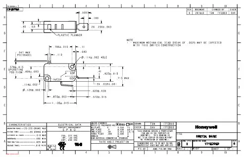
V7-1Z29E9;中文规格书,Datasheet资料
- 格式:pdf
- 大小:110.68 KB
- 文档页数:2
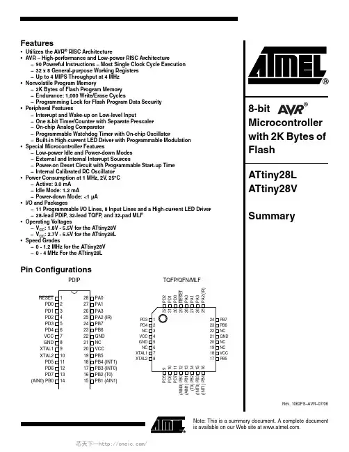
1Features•Utilizes the AVR ® RISC Architecture•AVR – High-performance and Low-power RISC Architecture–90 Powerful Instructions – Most Single Clock Cycle Execution –32 x 8 General-purpose Working Registers –Up to 4 MIPS Throughput at 4 MHz •Nonvolatile Program Memory–2K Bytes of Flash Program Memory –Endurance: 1,000 Write/Erase Cycles–Programming Lock for Flash Program Data Security •Peripheral Features–Interrupt and Wake-up on Low-level Input–One 8-bit Timer/Counter with Separate Prescaler –On-chip Analog Comparator–Programmable Watchdog Timer with On-chip Oscillator–Built-in High-current LED Driver with Programmable Modulation •Special Microcontroller Features–Low-power Idle and Power-down Modes –External and Internal Interrupt Sources–Power-on Reset Circuit with Programmable Start-up Time –Internal Calibrated RC Oscillator •Power Consumption at 1 MHz, 2V , 25°C –Active: 3.0 mA –Idle Mode: 1.2 mA–Power-down Mode: <1 µA •I/O and Packages–11 Programmable I/O Lines, 8 Input Lines and a High-current LED Driver –28-lead PDIP , 32-lead TQFP , and 32-pad MLF •Operating Voltages–V CC : 1.8V - 5.5V for the ATtiny28V –V CC : 2.7V - 5.5V for the ATtiny28L •Speed Grades–0 - 1.2 MHz for the ATtiny28V –0 - 4 MHz For the ATtiny28LPin ConfigurationsPDIPTQFP/QFN/MLF8-bit Microcontroller with 2K Bytes of ATtiny28L ATtiny28V SummaryNote: This is a summary document. A complete documentis available on our Web site at .2ATtiny28L/V1062FS–AVR–07/06DescriptionThe ATtiny28 is a low-power CMOS 8-bit microcontroller based on the AVR RISC archi-tecture. By executing powerful instructions in a single clock cycle, the ATtiny28 achieves throughputs approaching 1 MIPS per MHz, allowing the system designer to optimize power consumption versus processing speed. The AVR core combines a rich instruction set with 32 general-purpose working registers. All the 32 registers are directly con-nected to the Arithmetic Logic Unit (ALU), allowing two independent registers to be accessed in one single instruction executed in one clock cycle. The resulting architec-ture is more code efficient while achieving throughputs up to ten times faster than conventional CISC microcontrollers.Block DiagramFigure 1. The ATtiny28 Block DiagramThe ATtiny28 provides the following features: 2K bytes of Flash, 11 general-purpose I/O lines, 8 input lines, a high-current LED driver, 32 general-purpose working registers, an 8-bit timer/counter, internal and external interrupts, programmable Watchdog Timer with internal oscillator and 2 software-selectable power-saving modes. The Idle Mode stops the CPU while allowing the timer/counter and interrupt system to continue functioning.The Power-down mode saves the register contents but freezes the oscillator, disabling all other chip functions until the next interrupt or hardware reset. The wake-up or inter-3ATtiny28L/V1062FS–AVR–07/06rupt on low-level input feature enables the ATtiny28 to be highly responsive to external events, still featuring the lowest power consumption while in the power-down modes.The device is manufactured using Atmel’s high-density, nonvolatile memory technology.By combining an enhanced RISC 8-bit CPU with Flash on a monolithic chip, the Atmel ATtiny28 is a powerful microcontroller that provides a highly flexible and cost-effective solution to many embedded control applications. The ATtiny28 AVR is supported with a full suite of program and system development tools including: macro assemblers, pro-gram debugger/simulators, in-circuit emulators and evaluation kits.Pin DescriptionsVCC Supply voltage pin.GNDGround pin.Port A (PA3..PA0)Port A is a 4-bit I/O port. PA2 is output-only and can be used as a high-current LED driver. At V CC = 2.0V, the PA2 output buffer can sink 25 mA. PA3, PA1 and PA0 are bi-directional I/O pins with internal pull-ups (selected for each bit). The port pins are tri-stated when a reset condition becomes active, even if the clock is not running.Port B (PB7..PB0)Port B is an 8-bit input port with internal pull-ups (selected for all Port B pins). Port B pins that are externally pulled low will source current if the pull-ups are activated.Port B also serves the functions of various special features of the ATtiny28 as listed on page 27. If any of the special features are enabled, the pull-up(s) on the corresponding pin(s) is automatically disabled. The port pins are tri-stated when a reset condition becomes active, even if the clock is not running.Port D (PD7..PD0)Port D is an 8-bit I/O port. Port pins can provide internal pull-up resistors (selected for each bit). The port pins are tri-stated when a reset condition becomes active, even if the clock is not running.XTAL1Input to the inverting oscillator amplifier and input to the internal clock operating circuit.XTAL2Output from the inverting oscillator amplifier.pulses longer than 50 ns will generate a reset, even if the clock is not running. Shorter pulses are not guaranteed to generate a reset.4ATtiny28L/V1062FS–AVR–07/06Notes:1.For compatibility with future devices, reserved bits should be written to zero if accessed. Reserved I/O memory addressesshould never be written.2.Some of the status flags are cleared by writing a logical “1” to them. Note that the CBI and SBI instructions will operate on allbits in the I/O register, writing a one back into any flag read as set, thus clearing the flag. The CBI and SBI instructions work with registers $00 to $1F only.Register SummaryAddressNameBit 7Bit 6Bit 5Bit 4Bit 3Bit 2Bit 1Bit 0Page$3F SREG ITHSVNZCpage 6$3E Reserved ...Reserved $20Reserved $1F Reserved $1E Reserved $1D Reserved $1C Reserved $1B PORTA ----PORTA3PORTA2PORTA1PORTA0page 32$1A PACR ----DDA3PA2HCDDA1DDA0page 32$19PINA ----PINA3-PINA1PINA0page 32$18Reserved $17Reserved $16PINB PINB7PINB6PINB5PINB4PINB3PINB2PINB1PINB0page 32$15Reserved $14Reserved $13Reserved $12PORTD PORTD7PORTD6PORTD5PORTD4PORTD3PORTD2PORTD1PORTD0page 33$11DDRD DDD7DDD6DDD5DDD4DDD3DDD2DDD1DDD0page 33$10PIND PIND7PIND6PIND5PIND4PIND3PIND2PIND1PIND0page 33$0F Reserved $0E Reserved $0D Reserved $0C Reserved $0B Reserved $0A Reserved $09Reserved $08ACSR ACD -ACO ACI ACIE -ACIS1ACIS0page 44$07MCUCS PLUPB -SE SM WDRF -EXTRF PORF page 19$06ICR INT1INT0LLIE TOIE0ISC11ISC10ISC01ISC00page 22$05IFR INTF1INTF0-TOV0----page 23$04TCCR0FOV0--OOM01OOM00CS02CS01CS00page 35$03TCNT0Timer/Counter0 (8-bit)page 36$02MODCR ONTIM4ONTIM3ONTIM2ONTIM1 ONTIM0MCONF2MCONF1MCONF0page 43$01WDTCR ---WDTOEWDEWDP2WDP1WDP0page 37$00OSCCALOscillator Calibration Registerpage 95ATtiny28L/V1062FS–AVR–07/06Instruction Set SummaryMnemonicOperandsDescriptionOperationFlags# ClocksARITHMETIC AND LOGIC INSTRUCTIONSADD Rd, Rr Add Two RegistersRd ← Rd + Rr Z,C,N,V,H 1ADC Rd, Rr Add with Carry Two Registers Rd ← Rd + Rr + C Z,C,N,V,H 1SUB Rd, Rr Subtract Two Registers Rd ← Rd - Rr Z,C,N,V,H 1SUBI Rd, K Subtract Constant from Register Rd ← Rd - K Z,C,N,V,H 1SBC Rd, Rr Subtract with Carry Two Registers Rd ← Rd - Rr - C Z,C,N,V,H 1SBCI Rd, K Subtract with Carry Constant from Reg.Rd ← Rd - K - C Z,C,N,V,H 1AND Rd, Rr Logical AND RegistersRd ← Rd • Rr Z,N,V 1ANDI Rd, K Logical AND Register and Constant Rd ← Rd • K Z,N,V 1OR Rd, Rr Logical OR RegistersRd ← Rd v Rr Z,N,V 1ORI Rd, K Logical OR Register and Constant Rd ← Rd v K Z,N,V 1EOR Rd, Rr Exclusive OR Registers Rd ← Rd ⊕ Rr Z,N,V 1COM Rd One’s Complement Rd ← $FF - Rd Z,C,N,V 1NEG Rd Two’s Complement Rd ← $00 - Rd Z,C,N,V,H 1SBR Rd, K Set Bit(s) in Register Rd ← Rd v K Z,N,V 1CBR Rd, K Clear Bit(s) in Register Rd ← Rd • (FFh - K)Z,N,V 1INC Rd Increment Rd ← Rd + 1Z,N,V 1DEC Rd DecrementRd ← Rd - 1 Z,N,V 1TST Rd Test for Zero or Minus Rd ← Rd • Rd Z,N,V1CLR Rd Clear Register Rd ← Rd ⊕ Rd Z,N,V 1SER Rd Set Register Rd ← $FF None 1BRANCH INSTRUCTIONSRJMP k Relative JumpPC ← PC + k + 1None 2RCALL kRelative Subroutine Call PC ← PC + k + 1None 3RET Subroutine Return PC ← STACK None 4RETI Interrupt Return PC ← STACKI 4CPSE Rd, Rr Compare, Skip if Equal if (Rd = Rr) PC ← PC + 2 or 3None 1/2CP Rd, Rr CompareRd - Rr Z,N,V,C,H 1CPC Rd, Rr Compare with CarryRd - Rr - C Z,N,V,C,H 1CPI Rd, K Compare Register with Immediate Rd - KZ N,V,C,H 1SBRC Rr, b Skip if Bit in Register Cleared if (Rr(b) = 0) PC ← PC + 2 or 3None 1/2SBRS Rr, b Skip if Bit in Register is Set if (Rr(b) = 1) PC ← PC + 2 or 3None 1/2SBIC P, b Skip if Bit in I/O Register Cleared if (P(b) = 0) PC ← PC + 2 or 3None 1/2SBIS P, b Skip if Bit in I/O Register is Set if (P(b) = 1) PC ← PC + 2 or 3None 1/2BRBS s, k Branch if Status Flag Set if (SREG(s) = 1) then PC ← PC + k + 1None 1/2BRBC s, k Branch if Status Flag Cleared if (SREG(s) = 0) then PC ← PC + k + 1None 1/2BREQ k Branch if Equal if (Z = 1) then PC ← PC + k + 1None 1/2BRNE k Branch if Not Equal if (Z = 0) then PC ← PC + k + 1None 1/2BRCS k Branch if Carry Set if (C = 1) then PC ← PC + k + 1None 1/2BRCC k Branch if Carry Cleared if (C = 0) then PC ← PC + k + 1None 1/2BRSH k Branch if Same or Higher if (C = 0) then PC ← PC + k + 1None 1/2BRLO k Branch if Lower if (C = 1) then PC ← PC + k + 1None 1/2BRMI k Branch if Minus if (N = 1) then PC ← PC + k + 1None 1/2BRPL k Branch if Plusif (N = 0) then PC ← PC + k + 1None 1/2BRGE k Branch if Greater or Equal, Signed if (N ⊕ V = 0) then PC ← PC + k + 1None 1/2BRLT k Branch if Less than Zero, Signed if (N ⊕ V = 1) then PC ← PC + k + 1None 1/2BRHS k Branch if Half-carry Flag Set if (H = 1) then PC ← PC + k + 1None 1/2BRHC k Branch if Half-carry Flag Cleared if (H = 0) then PC ← PC + k + 1None 1/2BRTS k Branch if T-flag Set if (T = 1) then PC ← PC + k + 1None 1/2BRTC k Branch if T-flag Cleared if (T = 0) then PC ← PC + k + 1None 1/2BRVS k Branch if Overflow Flag is Set if (V = 1) then PC ← PC + k + 1None 1/2BRVC k Branch if Overflow Flag is Cleared if (V = 0) then PC ← PC + k + 1None 1/2BRIE k Branch if Interrupt Enabled if (I = 1) then PC ← PC + k + 1None 1/2BRIDkBranch if Interrupt Disabledif (I = 0) then PC ← PC + k + 1None1/26ATtiny28L/V1062FS–AVR–07/06DATA TRANSFER INSTRUCTIONSLD Rd, Z Load Register Indirect Rd ← (Z)None 2ST Z, Rr Store Register Indirect (Z) ← Rr None 2MOV Rd, Rr Move between Registers Rd ← Rr None 1LDI Rd, K Load Immediate Rd ←K None 1IN Rd, P In Port Rd ← P None 1OUT P, RrOut PortP ← Rr None 1LPMLoad Program MemoryR0 ← (Z)None3BIT AND BIT-TEST INSTRUCTIONS SBI P, b Set Bit in I/O Register I/O(P,b) ← 1None 2CBI P, b Clear Bit in I/O Register I/O(P,b) ←None 2LSL Rd Logical Shift LeftRd(n+1) ← Rd(n), Rd(0) ← 0Z,C,N,V 1LSR Rd Logical Shift Right Rd(n) ← Rd(n+1), Rd(7) ← 0Z,C,N,V 1ROL Rd Rotate Left through Carry Rd(0) ← C, Rd(n+1) ← Rd(n), C ← Rd(7)Z,C,N,V 1ROR Rd Rotate Right through Carry Rd(7) ← C, Rd(n) ← Rd(n+1), C ← Rd(0)Z,C,N,V 1ASR Rd Arithmetic Shift Right Rd(n) ← Rd(n+1), n = 0..6Z,C,N,V 1SWAP Rd Swap Nibbles Rd(3..0) ← Rd(7..4), Rd(7..4) ← Rd(3..0)None 1BSET s Flag Set SREG(s) ← 1SREG(s)1BCLR s Flag Clear SREG(s) ← 0SREG(s)1BST Rr, b Bit Store from Register to T T ← Rr(b)T 1BLD Rd, bBit Load from T to Register Rd(b) ← T None 1SEC Set Carry C ← 1C 1CLC Clear Carry C ←0C 1SEN Set Negative Flag N ← 1N 1CLN Clear Negative Flag N ← 0N 1SEZ Set Zero Flag Z ←1Z 1CLZ Clear Zero Flag Z ← 0Z1SEI Global Interrupt Enable I ← 1I 1CLI Global Interrupt Disable I ←I 1SES Set Signed Test FlagS ← 1S 1CLS Clear Signed Test Flag S ←0S 1SEV Set Two’s Complement OverflowV ←1V 1CLV Clear Two’s Complement Overflow V ← 0V 1SET Set T in SREG T ← 1T 1CLT Clear T in SREG T ← 0T 1SEH Set Half-carry Flag in SREG H ← 1H 1CLH Clear Half-carry Flag in SREG H ←H 1NOP No Operation None 1SLEEP Sleep(see specific descr. for Sleep function)None 1WDRWatchdog Reset(see specific descr. for WDR/timer)None1Instruction Set Summary (Continued)MnemonicOperandsDescriptionOperationFlags# Clocks7ATtiny28L/V1062FS–AVR–07/06Notes:1.This device can also be supplied in wafer form. Please contact your local Atmel sales office for detailed ordering informationand minimum quantities.2.Pb-free packaging alternative, complies to the European Directive for Restriction of Hazardous Substances (RoHS direc-tive).Also Halide free and fully Green.Ordering InformationSpeed (MHz)Power Supply (Volts)Ordering Code Package (1)Operation Range 42.7 - 5.5A Ttiny28L-4AC A Ttiny28L-4PC A Ttiny28L-4MC32A 28P332M1-A Commercial (0°C to 70°C)A Ttiny28L-4AI A Ttiny28L-4AU (2)A Ttiny28L-4PI A Ttiny28L-4PU (2)A Ttiny28L-4MI A Ttiny28L-4MU (2)32A 32A 28P328P332M1-A 32M1-A Industrial (-40°C to 85°C)1.21.8 - 5.5A Ttiny28V-1AC A Ttiny28V-1PC A Ttiny28V-1MC32A 28P332M1-A Commercial (0°C to 70°C)A Ttiny28V-1AI A Ttiny28V-1AU (2)A Ttiny28V-1PI A Ttiny28V-1PU (2)A Ttiny28V-1MI A Ttiny28V-1MU (2)32A 32A 28P328P332M1-A 32M1-AIndustrial (-40°C to 85°C)Package Type32A 32-lead, Thin (1.0 mm) Plastic Quad Flat Package (TQFP)28P328-lead, 0.300" Wide, Plastic Dual Inline Package (PDIP)32M1-A32-pad, 5x5x1.0 body, Lead Pitch 0.50mm, Quad Flat No-lead/Micro Lead Frame Package (QFN/MLF)8ATtiny28L/V1062FS–AVR–07/06Packaging Information32A9ATtiny28L/V1062FS–AVR–07/0628P310ATtiny28L/V1062FS–AVR–07/0632M1-A11ATtiny28L/V1062FS–AVR–07/06ErrataAll revisionsNo known errata.12ATtiny28L/V1062FS–AVR–07/06Datasheet Revision HistoryPlease note that the referring page numbers in this section are referred to this docu-ment. The referring revision in this section are referring to the document revision.Rev – 01/06G 1.Updated chapter layout.2.Updated “Ordering Information” on page 7.Rev – 01/06G1.Updated description for “Port A” on page 25.2.Added note 6 in “DC Characteristics” on page 54.3.Updated “Ordering Information” on page 7.4.Added “Errata” on page 11.Rev – 03/05F1.Updated “Electrical Characteristics” on page 54.2.MLF-package alternative changed to “Quad Flat No-Lead/Micro Lead Frame PackageQFN/MLF”.3.Updated “Ordering Information” on page 7.1062FS–AVR–07/06© 2006 Atmel Corporation . All rights reserved. ATMEL ®, logo and combinations thereof, Everywhere You Are ®, AVR ®, AVR Studio ®, and oth-ers, are registered trademarks or trademarks of Atmel Corporation or its subsidiaries. Other terms and product names may be trademarks of oth-ers.Disclaimer: The information in this document is provided in connection with Atmel products. No license, express or implied, by estoppel or otherwise,to any intellectual property right is granted by this document or in connection with the sale of Atmel products. EXCEPT AS SET FORTH IN ATMEL’S TERMS AND CONDI-TIONS OF SALE LOCATED ON ATMEL’S WEB SITE, ATMEL ASSUMES NO LIABILITY WHATSOEVER AND DISCLAIMS ANY EXPRESS, IMPLIED OR STATUTORY WARRANTY RELATING TO ITS PRODUCTS INCLUDING, BUT NOT LIMITED TO, THE IMPLIED WARRANTY OF MERCHANTABILITY, FITNESS FOR A PARTICULAR PURPOSE, OR NON-INFRINGEMENT. IN NO EVENT SHALL ATMEL BE LIABLE FOR ANY DIRECT, INDIRECT, CONSEQUENTIAL, PUNITIVE, SPECIAL OR INCIDEN-TAL DAMAGES (INCLUDING, WITHOUT LIMITATION, DAMAGES FOR LOSS OF PROFITS, BUSINESS INTERRUPTION, OR LOSS OF INFORMATION) ARISING OUT OF THE USE OR INABIL ITY TO USE THIS DOCUMENT, EVEN IF ATMEL HAS BEEN ADVISED OF THE POSSIBIL ITY OF SUCH DAMAGES. Atmel makes no representations or warranties with respect to the accuracy or completeness of the contents of this document and reserves the right to make changes to specifications and product descriptions at any time without notice. Atmel does not make any commitment to update the information contained herein. Unless specifically provided otherwise, Atmel products are not suitable for, and shall not be used in, automotive applications. Atmel’s products are not intended, authorized, or warranted for use as components in applications intended to support or sustain life.Atmel CorporationAtmel Operations2325 Orchard Parkway San Jose, CA 95131, USA Tel: 1(408) 441-0311Fax: 1(408) 487-2600Regional HeadquartersEuropeAtmel SarlRoute des Arsenaux 41Case Postale 80CH-1705 Fribourg SwitzerlandTel: (41) 26-426-5555Fax: (41) 26-426-5500AsiaRoom 1219Chinachem Golden Plaza 77 Mody Road Tsimshatsui East Kowloon Hong KongTel: (852) 2721-9778Fax: (852) 2722-1369Japan9F, Tonetsu Shinkawa Bldg.1-24-8 ShinkawaChuo-ku, Tokyo 104-0033JapanTel: (81) 3-3523-3551Fax: (81) 3-3523-7581Memory2325 Orchard Parkway San Jose, CA 95131, USA Tel: 1(408) 441-0311Fax: 1(408) 436-4314Microcontrollers2325 Orchard Parkway San Jose, CA 95131, USA Tel: 1(408) 441-0311Fax: 1(408) 436-4314La Chantrerie BP 7060244306 Nantes Cedex 3, France Tel: (33) 2-40-18-18-18Fax: (33) 2-40-18-19-60ASIC/ASSP/Smart CardsZone Industrielle13106 Rousset Cedex, France Tel: (33) 4-42-53-60-00Fax: (33) 4-42-53-60-011150 East Cheyenne Mtn. Blvd.Colorado Springs, CO 80906, USA Tel: 1(719) 576-3300Fax: 1(719) 540-1759Scottish Enterprise Technology Park Maxwell BuildingEast Kilbride G75 0QR, Scotland Tel: (44) 1355-803-000Fax: (44) 1355-242-743RF/AutomotiveTheresienstrasse 2Postfach 353574025 Heilbronn, Germany Tel: (49) 71-31-67-0Fax: (49) 71-31-67-23401150 East Cheyenne Mtn. Blvd.Colorado Springs, CO 80906, USA Tel: 1(719) 576-3300Fax: 1(719) 540-1759Biometrics/Imaging/Hi-Rel MPU/High Speed Converters/RF DatacomAvenue de Rochepleine BP 12338521 Saint-Egreve Cedex, France Tel: (33) 4-76-58-30-00Fax: (33) 4-76-58-34-80Literature Requests/literature。


RF Power Field Effect TransistorN--Channel Enhancement--Mode Lateral MOSFETDesigned for pulsed wideband applications operating at frequencies between 3100and 3500MHz.•Typical Pulsed Performance:V DD =32Volts,I DQ =50mA,P out =15Watts Peak (3Watts Avg.),Pulsed Signal,f =3500MHz,Pulse Width =100μsec,Duty Cycle =20%Power Gain —16dB Drain Efficiency —41%•Typical WiMAX Performance:V DD =32Volts,I DQ =150mA,P out =1.8Watts Avg.,f =3500MHz,802.16d,64QAM 3/4,4Bursts,10MHz Channel Bandwidth,Input Signal PAR =9.5dB @0.01%Probability on CCDF Power Gain —18dB Drain Efficiency —16%RCE —--33dB (EVM —2.2%rms)•Capable of Handling 10:1VSWR,@32Vdc,3300MHz,15Watts Peak Power•Capable of Handling 3dB Overdrive @32Vdc Features•Characterized with Series Equivalent Large--Signal Impedance Parameters •Internally Matched for Ease of Use •Integrated ESD Protection•Greater Negative Gate--Source Voltage Range for Improved Class C Operation•RoHS Compliant•In Tape and Reel.R3Suffix =250Units,32mm Tape Width,13inch Reel.Table 1.Maximum RatingsRatingSymbol Value Unit Drain--Source Voltage V DSS --0.5,+65Vdc Gate--Source Voltage V GS --6.0,+10Vdc Operating VoltageV DD 32,+0Vdc Storage Temperature Range T stg --65to +150°C Case Operating Temperature T C 150°C Operating Junction Temperature (1,2)T J225°CTable 2.Thermal CharacteristicsCharacteristicSymbol Value (2,3)Unit Thermal Resistance,Junction to CaseCase Temperature 80°C,15W Pulsed,100μsec Pulse Width,20%Duty Cycle Case Temperature 81°C,15W Pulsed,500μsec Pulse Width,10%Duty CycleR θJC0.600.73°C/W1.Continuous use at maximum temperature will affect MTTF.2.MTTF calculator available at /rf.Select Software &Tools/Development Tools/Calculators to access MTTF calculators by product.3.Refer to AN1955,Thermal Measurement Methodology of RF Power Amplifiers.Go to /rf.Select Documentation/Application Notes --AN1955.Document Number:MRF7S35015HSRev.2,4/2011Freescale Semiconductor Technical DataMRF7S35015HSR3Table 3.ESD Protection CharacteristicsTest MethodologyClass Human Body Model (per JESD22--A114)1B (Minimum)Machine Model (per EIA/JESD22--A115)A (Minimum)Charge Device Model (per JESD22--C101)IV (Minimum)Table 4.Electrical Characteristics (T C =25°C unless otherwise noted)CharacteristicSymbolMinTypMaxUnitOff CharacteristicsGate--Source Leakage Current (V GS =5Vdc,V DS =0Vdc)I GSS ——1μAdc Zero Gate Voltage Drain Leakage Current (V DS =32Vdc,V GS =0Vdc)I DSS ——2μAdc Zero Gate Voltage Drain Leakage Current (V DS =65Vdc,V GS =0Vdc)I DSS——10μAdcOn CharacteristicsGate Threshold Voltage(V DS =10Vdc,I D =33.5μAdc)V GS(th) 1.22 2.7Vdc Gate Quiescent Voltage(V DD =32Vdc,I D =50mAdc,Measured in Functional Test)V GS(Q) 1.8 2.5 3.3Vdc Drain--Source On--Voltage(V GS =10Vdc,I D =300mAdc)V DS(on)0.11.70.3VdcDynamic Characteristics (1)Reverse Transfer Capacitance(V DS =32Vdc ±30mV(rms)ac @1MHz,V GS =0Vdc)C rss —0.12—pF Output Capacitance(V DS =32Vdc ±30mV(rms)ac @1MHz,V GS =0Vdc)C oss —92—pF Input Capacitance(V DS =32Vdc,V GS =0Vdc ±30mV(rms)ac @1MHz)C iss—46—pFFunctional Tests (In Freescale Test Fixture,50ohm system)V DD =32Vdc,I DQ =50mA,P out =15W Peak (3W Avg.),f =3100MHz and f =3500MHz,Pulsed,100μsec Pulse Width,20%Duty Cycle,25ns Input Rise Time Power Gain G ps 131619dB Drain Efficiency ηD 3841—%Input Return LossIRL—--12--7dBPulsed RF Performance (In Freescale Application Test Fixture,50ohm system)V DD =32Vdc,I DQ =50mA,P out =15W Peak (3W Avg.),f =3100MHz and f =3500MHz,Pulsed,100μsec Pulse Width,20%Duty Cycle,25ns Input Rise Time Output Pulse Droop(500μsec Pulse Width,10%Duty Cycle)DRP out —0.2—dBLoad Mismatch Tolerance(VSWR =10:1at all Phase Angles)VSWR--TNo Degradation in Output Power1.Part internally matched both on input and output.MRF7S35015HSR3Z180.078″x 0.454″Microstrip Z190.055″x 0.244″Microstrip Z200.630″x 0.073″Microstrip Z210.218″x 0.038″Microstrip Z220.060″x 0.552″Microstrip Z230.079″x 0.038″Microstrip Z240.062″x 0.526″Microstrip Z250.032″x 0.070″Microstrip Z260.110″x 0.526″Microstrip Z270.053″x 0.072″Microstrip Z280.028″x 0.070″Microstrip Z290.098″x 0.148″Microstrip Z300.062″x 0.526″Microstrip Z310.529″x 0.070″MicrostripPCBArlon CuClad 250GX--0300--55--22,0.030″,εr =2.55*Line length includes microstrip bendsZ10.375″x 0.071″Microstrip Z20.126″x 0.524″Microstrip Z30.079″x 0.016″Microstrip Z40.153″x 0.071″Microstrip Z50.076”x 0.520″Microstrip Z60.037″x 0.252″Microstrip Z70.322″x 0.073″Microstrip Z80.123″x 0.440″Microstrip Z90.048″x 0.073″Microstrip Z100.081″x 0.184″Microstrip Z110.030″x 0.262″Microstrip Z120.525″x 0.336″Microstrip Z130.182″x 0.466″Microstrip Z140.077″x 0.466″Microstrip Z15*0.603″x 0.048″Microstrip Z160.063″x 0.618″Microstrip Z17*0.534″x 0.040″MicrostripFigure 1.MRF7S35015HSR3Test Circuit SchematicTable 5.MRF7S35015HSR3Test Circuit Component Designations and ValuesPartDescriptionPart NumberManufacturer B1*Long Ferrite Bead 2743021447Fair--Rite B2,B3Short Ferrite Beads2743019447Fair--Rite C1470μF,63V Electrolytic Capacitor 477KXM063M Illinois Cap C247μF,50V Electrolytic Capacitor 476KXM050M Illinois Cap C3,C922μF,35V Tantalum Capacitors T491X226K035AT Kemet C4,C5,C10 2.7pF Chip Capacitors ATC100B2R7BT500XT ATC C60.8pF Chip Capacitor ATC100B0R8BT500XT ATC C70.1μF Chip CapacitorCDR33BX104AKYS AVX C822μF,25V Tantalum CapacitorT491D226K025ATKemet*B1is removed for WiMAX circuit performance.MRF7S35015HSR3Figure2.MRF7S35015HSR3Test Circuit ComponentLayoutMRF7S35015HSR3TYPICAL CHARACTERISTICS0.11000C ,C A P A C I T A N C E (p F )101100G p s ,P O W E R G A I N (d B )132011716P out ,OUTPUT POWER (WATTS)PULSEDFigure 7.Pulsed Power Gain versusOutput Power G p s ,P O W E R G A I N (d B )101530Figure 8.Pulsed Power Gain versusOutput PowerP out ,OUTPUT POWER (WATTS)PULSED11030141819MRF7S35015HSR3TYPICAL CHARACTERISTICS0302015P o u t ,O U T P U T P O W E R (W A T T S )P U L S E D251050605030ηD ,D R A I N E F F I C I E N C Y (%)4020101P out ,OUTPUT POWER (WATTS)PULSEDFigure 12.Pulsed Power Gain and Drain Efficiencyversus Output Power —3500MHz3010MRF7S35015HSR3TYPICAL CHARACTERISTICS15.2517.25--36444341G p s ,P O W E R G A I N (d B )ηD ,D R A I N E F F I C I E N C Y (%)174216.251615.7515.5--2716.7516.5--18--9I R L ,I N P U T R E T U R N L O S S (d B )18G A I N (d B )28P out ,OUTPUT POWER (dBm)Figure 14.Single--Channel OFDM Relative Constellation Error,Drain Efficiency and Gain versus Output Power17.918.318.218.1--45--25--27--294242220181412108ηD ,D R A I N E F F I C I E N C Y (%)R C E (R E L A T I V E C O N S T E L L A T I O N E R R O R (d B )--31--33--37--39--41--4329303132333616617.8--35343525010890T J ,JUNCTION TEMPERATURE (°C)Figure 15.MTTF versus Junction TemperatureThis above graph displays calculated MTTF in hours when the device is operated at V DD =32Vdc,P out =15W Peak,Pulse Width =100μsec,Duty Cycle =20%,and ηD =41%.MTTF calculator available at /rf.Select Software &Tools/Development Tools/Calculators to access MTTF calculators by product.107106105110130150170190M T T F (H O U R S )210230MRF7S35015HSR3Z o=50ΩZ loadf=3500MHzf=3100MHzZ sourcef=3100MHzf=3500MHzV DD=32Vdc,I DQ=50mA,P out=15W PeakfMHzZ sourceΩZ loadΩ310048.6+j16.1 5.6--j5.2330011.8+j3.15 6.36--j6.833500 6.43--j6.797.41--j15.5Z source=Test circuit impedance as measured fromgate to ground.Z load=Test circuit impedance as measuredfrom drain to ground.Figure16.Series Equivalent Source and Load ImpedanceZ source Z loadOutputMatchingNetworkMRF7S35015HSR3PACKAGEDIMENSIONSMRF7S35015HSR3分销商库存信息:FREESCALEMRF7S35015HSR3MRF7S35015HSR5。
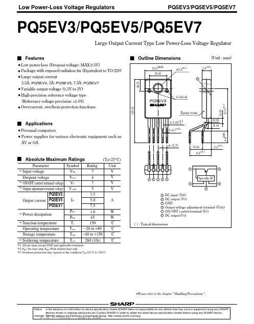
Low Power-Loss Voltage Regulators PQ5EV3/PQ5EV5/PQ5EV7PQ5EV3/PQ5EV5/PQ5EV7Large Output Current Type Low Power-Loss Voltage Regulators Outline Dimensions(Unit : mm)s Featuresq Low power-loss (Dropout voltage: MAX.0.5V)q Package with exposed radiation fin (Equivalent to TO-220) q Large output current3.5A: PQ5EV3, 5A: PQ5EV5, 7.5A: PQ5EV7 q Variable output voltage (1.5V to 5V) q High-precision reference voltage type (Reference voltage precision: ±1.0%)q Overcurrent, overheat protection functionss Applicationsq Personal computersq Power supplies for various electronic equipment such as AV or OAs Absolute Maximum Ratings•Please refer to the chapter " Handling Precautions ".ParameterSymbol Rating UnitInput voltage7V 5.0A 7.5475V V V 3.5Output current 1.6W 45W 150˚C Power dissipationDropout voltageON/OFF control terminal voltageOutput adjustment terminal voltage V IN V I-O V C V ADJI O P D2P D1(Ta =25°C)Junction temperature Operating temperature Storage temperature Soldering temperature T j −20 to +80˚C T opr −40 to +150˚C T stg 260 (10s)˚CT sol ❇1❇1❇1❇3❇4❇2❇1 All are open except GND and applicable terminals ❇2 P D1:No heat sink, P D2:With infinite heat sink❇3 Overheat protection may operate at the condition T j =125˚C to 150˚CPQ5EV3PQ5EV5PQ5EV72.35−71.51.2276−1.24−0.10.5−0.050.1−60−−−−−±170−−−ParameterMIN.TYP.MAX.Conditions (Unless otherwise specified, V IN =5V, ❇4,V O =3V (R 1=2k Ω) , Ta=25˚C)−−I O =5mA to rating V IN =4 to 7V, I O =5mA Refer to Fig.2−V C =2.7V−−T j =0 to 125˚C ❇5❇6V C =0.4VI O =0A2−51.2524−−0.5−200.8−0.4Input voltage Load regulation Line regulationReference voltage temperature coefficient Ripple Rejection Dropout voltageON-state voltage for control OFF-state voltage for control OFF-state current for control Quiescent currentON-state current for control Output voltage Reference voltage 10V IN V O V ref R eg L R eg I T C V ref RR V C (ON)V I-O I C (ON)V C (OFF)I C (OFF)Symbol I qV V V %%dB %VV mA VµA UnitmA −15❇4 PQ5EV3:I O =1.75A, PQ5EV5:I O =2.5A, PQ5EV7:I O =3.75A❇5 PQ5EV3:I O =3.5A, PQ5EV5:I O =5A, PQ5EV7:I O =7.5A. Input voltage shall be the value when output voltage is 95% in comparison with the initial value ❇6 In case of opening control terminal ➄, output voltage turns on.V O =V ref × (1+R 2/R 1)[R 1=2k Ω, V ref .=. 1.24V]V eif =120Hz (sine wave)ei(rms)=0.5V V O =3V (R 1=2k Ω)V IN =5V I O =0.5ARR =20log (ei(rms)/eo(rms))1.6102030405045P o w e r d i s s i p a t i o n P D (W )Ambient temperature T a (˚C)Note) Oblique line portion:Overheat protection may operate in this area20406080100R e l a t i v e o u t p u t v o l t a g e (%)Output current I O (A)Low Power-Loss Voltage RegulatorsPQ5EV3/PQ5EV5/PQ5EV7Fig.5Overcurrent ProtectionCharacteristics (PQ5EV5)Fig.6Overcurrent ProtectionCharacteristics (PQ5EV7)Fig.7Reference Voltage Fluctuation vs.Junction TemperatureFig.8Output Voltage vs. Input Voltage(PQ5EV3)Fig.9Output Voltage vs. Input Voltage(PQ5EV5)Fig.10Output Voltage vs. Input Voltage(PQ5EV7)20406080100R e l a t i v e o u t p u t v o l t a g e (%)Output current I O (A)20406080100R e l a t i v e o u t p u t v o l t a g e (%)Output current I O (A)–10–8–6–4–20246810R e f e r e n c e v o l t a g e f l u c t u a t i o n ∆V r e f (m V )Junction temperature T j (˚C)01234O u t p u t v o l t a g e V O (V )Input voltage VIN (V)1234O u t p u t v o l t a g e V O (V )Input voltage VIN (V)01234O u t p u t v o l t a g e V O (V )Input voltage V IN (V)020406080100120140160C i r c u i t o p e r a t i n g c u r r e n t I B I A S (m A )Input voltage V IN (V)020406080100120140160C i r c u i t o p e r a t i n g c u r r e n t I B I A S (m A )Input voltage V IN (V)200406080100120140160C i r c u i t o p e r a t i n g c u r r e n t I B I A S (m A )Input voltage V IN (V)00.050.10.150.20.250.30.350.40.450.5D r o p o u t v o l t a g e V I -O (V )Junction temperature T j (˚C)0.20.40.60.811.21.41.61.82O N /O F F t h r e s h o l d v o l t a g e (V )Junction temperature T j (˚C)0.511.522.533.544.550Q u i e s c e n t c u r r e n t I q (m A )Junction temperature T j (˚C)Low Power-Loss Voltage RegulatorsPQ5EV3/PQ5EV5/PQ5EV7Fig.17Ripple Rejection vs. Input RippleFrequencyFig.18Output Voltage AdjustmentCharacteristicsFig.19External Connections Setting of Output VoltageOutput voltage is able to set (1.5V to 5V) when resistors R 1, R 2 are attached to ➁, ➂, ➃ terminals. As for the external resistors toset output voltage, refer to the following figure and Fig.18.01020304050607080 R i p p l er e j e c t i o n R R (d B )Input ripple frequency f (kHz)00.511.522.533.544.55O u t p u t v o l t a g e V O (V )R 2 (Ω)LoadONOTICEq The circuit application examples in this publication are provided to explain representative applications of SHARP devices and are not intended to guarantee any circuit design or license any intellectual property rights. SHARP takes no responsibility for any problems related to any intellectual property right of a third party resulting from the use of SHARP's devices.q Contact SHARP in order to obtain the latest device specification sheets before using any SHARP device. SHARP reserves the right to make changes in the specifications, characteristics, data, materials, structure, and other contents described herein at any time without notice in order to improve design or reliability. Manufacturing locations are also subject to change without notice.q Observe the following points when using any devices in this publication. SHARP takes no responsibility for damage caused by improper use of the devices which does not meet the conditions and absolute maximum ratings to be used specified in the relevant specification sheet nor meet the following conditions:(i)The devices in this publication are designed for use in general electronic equipment designs such as:--- Personal computers--- Office automation equipment--- Telecommunication equipment [terminal]--- Test and measurement equipment--- Industrial control--- Audio visual equipment--- Consumer electronics(ii)Measures such as fail-safe function and redundant design should be taken to ensure reliability and safety when SHARP devices are used for or in connection with equipment that requires higher reliability such as:--- Transportation control and safety equipment (i.e., aircraft, trains, automobiles, etc.)--- Traffic signals--- Gas leakage sensor breakers--- Alarm equipment--- Various safety devices, etc.(iii)SHARP devices shall not be used for or in connection with equipment that requires an extremely high level of reliability and safety such as:--- Space applications--- Telecommunication equipment [trunk lines]--- Nuclear power control equipment--- Medical and other life support equipment (e.g., scuba).q Contact a SHARP representative in advance when intending to use SHARP devices for any "specific" applications other than those recommended by SHARP or when it is unclear which category mentioned above controls the intended use.q If the SHARP devices listed in this publication fall within the scope of strategic products described in the Foreign Exchange and Foreign Trade Control Law of Japan, it is necessary to obtain approval to export such SHARP devices. q This publication is the proprietary product of SHARP and is copyrighted, with all rights reserved. Under the copyright laws, no part of this publication may be reproduced or transmitted in any form or by any means, electronic or mechanical, for any purpose, in whole or in part, without the express written permission of SHARP. Express written permission is also required before any use of this publication may be made by a third party.q Contact and consult with a SHARP representative if there are any questions about the contents of this publication.。