逻辑与计算机设计基础答案
- 格式:pdf
- 大小:40.10 KB
- 文档页数:3

数字逻辑习题1.仅用NOR门来构造下面函数的逻辑网络:H=(XY)’Z’
2.仅用NAND门来构造下面的函数的逻辑网络:D=(A+B)B’
3.求出由下面逻辑网络产生的函数G的最简单形式
4.卡诺图化简:G(A,B,C,D)=Σm(2,3,4,7,8,14,15)
5. 卡诺图化简:G(A,B,C,D)=Σm(0,1,3,4,6,7,12,13,14)
6.卡诺图化简:G(A,B,C,D)=Σm(0,4,5,6,7,8,13,14,15)
7.卡诺图化简:G(A,B,C,D)=Σm(1,2,3,4,6,7,9,12,13)
8.采用一个组合电路来控制一个十进制的七段显示,此电路有4个输入,并提供用压缩十进制数表示的4位代码(0(d)=0000,……8(d)=1000,9(d)=1001)。
7个输出用来定义哪段激活,以显示给定的十进制数
(1)写出这个电路的真值表
(2)用sop形式表示真值表
(3)用pos形式表示真值表
(4)写出各段化简的表达式
7.时序电路分析
补充:。


CHAPTER 6© 2008 Pearson Education, Inc.6-1.*6-2.6-3.6-4.*6-5.a) F = (A + B) C Db) G = (A + B) (C + D)a) 3-input NAND gate 6 inputs 16 inputs 16 inputsThe longest path is from input C or D.0.073 ns + 0.073 ns + 0.048 ns + 0.073 ns = 0.267 nsa)b)c)4.03.02.01.06.05.08.07.09.0 ns6-6.6-7. 6-8.+If the rejection time for inertial delays is greater than the propagation delay, then an output change can occur before it can be predicted whether or not it is to occur due to the rejection time.For example, with a delay of 2 ns and a rejection time of 3 ns, for a 2.5 ns pulse, the initialedge will have already appeared at the output before the 3 ns has elapsed at which whether to reject or not is to be determined.a) The propagation delay is t pd = max(t PHL = 0.05, t PLH = 0.10) = 0.10 ns.Assuming that the gate is an inverter, for a positive output pulse, the following actually occurs:If the input pulse is narrower than 0.05 ns, no output pulse occurs so the rejection time is 0.05 ns. The resulting model predicts the following results, which differ from the actual delay behavior, but models the rejection behavior: :0.10 ns0.05 ns0.10 ns0.10 ns6-9. 6-10.*b) For a negative output pulse, the following actually occurs:The model predicts the following results, which differs from the actual delay behavior andthe actual rejection behavior:Overall, the model is inaccurate for both cases a and b, and provides a faulty rejectionmodel for case b. Using an average of t PHL and t PLH for t pd would improve the delayaccuracy of the model for circuit applications, but the rejection model still fails.0.10 ns0.05 ns0.15 ns0.10 ns0.10 nsa)There is a setup time violation at 28 ns. There is an inputb)There is a setup time violation just before 24 ns, There is an inputc)There is a setup time violation at 28ns.d)There is a hold time violation at 16ns and a setup time violation at 24ns.combination violation around 24 ns.combination violation around 24 ns.a) The longest direct path delay is from input X through the two XOR gates to the output Y.t delay = t pdXOR + t pdXOR = 0.20 + 0.20 = 0.40 nsb) The longest path from an external input to a positive clock edge is from input X through the XOR gate and the inverter to the B Flip-flop.t delay = t pdXOR + t pd INV + t sFF = 0.20 + 0.05 + 0.1 = 0.35 nsc) The longest path delay from the positive clock edge is from Flip-flop A through the two XOR gates to the output Y.t delay = t pdFF + 2 t pdXOR = 0.40 + 2(0.20) = 0.80 nsd) The longest path delay from positive clock edge to positive clock edge is from clock on Flip-flop A through t delay-clock edge to clock edge = t pdFF + t pdXOR + t pdINV + t sFF = 0.40 + 0.20 + 0.05 + 0.10 = 0.75 nse) The maximum frequency is 1/t delay- clock edge to clock edge. For this circuit, t delay-clock edge to clock edgeis 0.75 ns, so the maximum frequency is 1/0.75 ns = 1.33 GHz.the XOR gate and inverter to clock on Flip-flop B.into its environment. Calculation of this frequency cannot be performed in this case since data for paths through the environment is not provided.Comment: The clock frequency may need to be lower due to other delay paths that pass outside of the circuit6-11.6-12.a) The longest direct path delay is from input X through the four XOR gates to the output Y.t delay = 4 t pdXOR = 4(0.20) = 0.80 nsb) The longest path from an external input to a positive clock edge is from input X through three XOR gates and the inverter to the clock of the second B Flip-flop.t delay = 3 t pdXOR + t pd INV + t sFF = 3(0.20) + 0.5 + 0.1 = 0.75 nsc) The longest path delay from the positive clock edge is from the first Flip-flop A through the four XOR gates to the output Y.t delay = t pdFF + 4 t pdXORR = 0.40 + 4(0.20) = 1.2 nsd) The longest path delay from positive clock edge to positive clock edge is from the first Flip-flop A through three XOR gates and one inverter to the clock of the second Flip-flop B.t delay-clock edge to clock edge = t pdFF + 3 t pdXOR + t pdINV + t sFF = 0.40+ 3(0.20) + 0.5 + 0.1 = 1.15 nse) The maximum frequency is 1/t delay-clock edge to clock edge. For this circuit, the delay is 1.15 nsso the maximum frequency is 1/1.15 ns = 870 MHz.Comment: The clock frequency may need to be lower due to other delay paths that pass outside of the circuit into its environment. Calculation of this frequency cannot be performed in this case since data for paths through the environment is not provided.AA6-13.*(Errata: Change "32 X 8" to "64 X 8" ROM)6-14. 6-15.6-16.IN OUT IN OUT IN OUT IN OUT 0000000000 00000100000001 01101000000011 00101100000100 1000 0000010000 00010100010001 01111000010011 00111100010100 1001 0000100000 00100100100001 10001000100011 01001100100101 0000 0000110000 00110100110001 10011000110011 01011100110101 0001 0001000000 01000101000010 00001001000011 01101101000101 0010 0001010000 01010101010010 00011001010011 01111101010101 0011 0001100000 01100101100010 00101001100011 10001101100101 0100 0001110000 01110101110010 00111001110011 10011101110101 0101 0010000000 10000110000010 01001010000100 00001110000101 0110 0010010000 10010110010010 01011010010100 00011110010101 0111 0010100001 00000110100010 01101010100100 00101110100101 1000 0010110001 00010110110010 01111010110100 00111110110101 1001 0011000001 00100111000010 10001011000100 01001111000110 0000 0011010001 00110111010010 10011011010100 01011111010110 0001 0011100001 01000111100011 00001011100100 01101111100110 0010 0011110001 01010111110011 00011011110100 01111111110110 0011a)16 + 16 + 1 = 33 address bits and 16 + 1 = 17 output bits, 8G × 17b)8 + 8 + 1 + 1 = 18 address bits and 8 + 1 = 9 output bitsc) 4 × 4 = 16 address bits and 14 output bits are needed, 64K × 14XYZXYZXYZXYZA B C D1111111111111111B = XY + XY + YZC = YZ C = YZ + Z A = XY + XY + YZBy using A instead of A and YZ instead of Y in D, YZ can be shared by all four functions. Further, since A is the complement of B, terms XY and XY can be shared between A and B. Thus, only four product terms YZ, XY, XY, and Z are required.An inversion must be programmed for A.6-17.6-18.6-19.*XY ZXYZ X YZ XY Z XYZ111111111X YZ 11AB CDEF11A = XYB = X + YZC = XY + X Y + ZD = YZE = 0F = ZImplementation of A, D, and E requires only two terms, XY and YZ. Straightforward implementation of B, C, and F requires four terms, XY , XYZ, XYZ, and Z. By implementing B, C, and F, only three additional termsX, X Y , and Z are required. So we form the solution using five product terms: XY , YZ, X Y, X, and Z. The solution is described by the equations given with the six K-maps.ABC D A BC D A BC D A BC D W X Y Z The values given in the four K-maps come from Table 3-1 on page 99.100110001100001111110000110011001111100d d d d dd d d d d dd d d d ddd d d d d dd W = A B + BC DX = BC D + BC + BD Y = CD + C D Z = D In this case, shared terms are limited. One such term B C D is generated in W.Assume 3-input OR gates.ABC DABC D ABCD ABC D W 100110001100001111110000110011001111100d d d d dd d d d ddd d d d ddd d d d d dd W = A + BC + BDX = BC D + BC + BD Y= CD + C D Z = D Each of the equations above is implemented using one 3-input OR gate. Four gates are used.6-20.6-21.X Y ZXYZX YZX Y Z11111111A B CD1A = XZ + YZ + X YZ B = XY + YZ + X YC = A + XYD = XY + Z1111111111Figure 6-23 uses 3-input OR gates.A, B, and D each require three or fewer product terms so can be implemented with 3-input OR gates.C requires four terms so cannot be implemented with a 3-input OR gate. But because the first PAL device outputcan used as an input to implement other functions it can be assigned to A and A can then be used to implement C using just two inputs of a 3-input OR gate.A ABCDABCD F111111111111111111GFigure 6-23 uses 3-input OR gates.Straightforward implementation of F requires five prime implicants and of G requires four prime implicants, but only 3 inputs are available on the PAL OR gates. So sum-of-products that can be factored from F and G or both and implemented by the other PAL cells are needed. A single sum of products that will work is H = ABC + BCD + BCD. The terms of H are shown with dotted lines on the K-maps. Using H:F = H + CD + ABG =H + AB There are other possible functions for H and corresponding results for F and H.。

逻辑与计算机设计基础第五版逻辑与计算机设计是现代计算机科学的基础课程之一,它包含了逻辑学和计算机设计的基本原理与方法。
本文将介绍《逻辑与计算机设计基础第五版》这本教材的内容和意义。
逻辑学是研究思维规律和推理方法的学科,它对于计算机科学的发展具有重要的理论基础作用。
《逻辑与计算机设计基础第五版》从逻辑学的基本概念和原理入手,介绍了命题逻辑、谓词逻辑、命题演算与谓词演算等内容。
通过学习这些内容,读者可以了解逻辑学的基本知识,掌握逻辑推理的方法和技巧,从而提高自己的思维能力和解决问题的能力。
计算机设计是指设计和构造计算机硬件和软件的过程。
《逻辑与计算机设计基础第五版》以计算机硬件设计为主线,介绍了数字电路的基本原理和设计方法。
它从二进制系统、布尔代数和逻辑门开始,逐步讲解了组合逻辑电路和时序逻辑电路的设计与分析。
通过学习这些内容,读者可以了解计算机硬件的工作原理,掌握数字电路的设计和分析方法,从而能够设计和构造简单的计算机硬件系统。
除了逻辑学和计算机设计的基本原理和方法,本书还介绍了一些与计算机科学密切相关的内容,如数据表示与运算、存储器和输入输出设备、指令系统和汇编语言、计算机组成与体系结构等。
这些内容为读者进一步学习和研究计算机科学的相关领域奠定了坚实的基础。
《逻辑与计算机设计基础第五版》在编写过程中遵循了逻辑与计算机设计的基本原理,确保了内容的准确性和严谨性。
本书采用了简洁明了的语言,避免了晦涩难懂的数学公式和计算公式,使读者更好地理解和掌握相关知识。
此外,本书还配有丰富的例题和习题,供读者练习和巩固所学知识。
《逻辑与计算机设计基础第五版》是一本理论与实践相结合的教材,它既介绍了逻辑学和计算机设计的基本原理和方法,又通过实例和习题的方式帮助读者掌握相关技能。
对于计算机科学专业的学生和从事计算机相关工作的人员来说,它是一本必不可少的参考书。
阅读本书可以帮助读者建立起扎实的逻辑思维和计算机设计的基础,为进一步学习和研究计算机科学奠定坚实的基础。
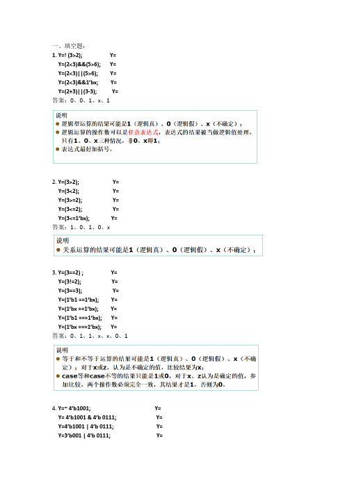
一、填空题:1. Y=! (3>2); Y=Y=(2<3)&&(5>6); Y=Y=(2<3)||(5>6); Y=Y=(2<3)&&1’bx; Y=Y=(2+3)||(3-3); Y=答案:0、0、1、x、12. Y=(3>2); Y=Y=(3<2); Y=Y=(3>=2); Y=Y=(3<=2); Y=Y=(3<=1’bx); Y=答案:1、0、1、0、x3. Y=(3==2) ; Y=Y=(3!=2); Y=Y=(3==3); Y=Y=(1’b1 ==1’bx); Y=Y=(1’bx ==1’bx); Y=Y=(1’b1 ===1’bx); Y=Y=(1’bx ===1’bx); Y=答案:0、1、1、x、x、0、14. Y=~ 4’b1001; Y= Y= 4’b1001 & 4’b 0111; Y= Y=4’b1001 | 4’b 0111; Y= Y=3’b001 | 4’b 0111; Y=Y=3’b001 | 4’b 0111 & 3’b101; Y=答案:0110、0001、1111、0111、01015. A=5’b11001&A=(((1&0)&0)&1)&1=?|A=?^A=(((1^0)^0)^1)^1=?答案:0、1、16. Y= 4’b1001 >> 1; Y=Y= 4’sb1001 >>> 1; Y=答案:0100、11007. Y= {4’b1001, 2’b11}; Y=Y= {4{2’b01}}; Y=Y= {{4{2’b01}}, 2’b11}; Y=答案:100111、01010101、010*******8. 例:二选一多路选择器module mux2_1(out,a,b,sel);output out;input a,b,sel;assign out=sel?b:aendmodule若sel为0则out =?;若sel为1则out = ?。

数字电路与逻辑设计习题答案数字电路与逻辑设计习题答案数字电路与逻辑设计是计算机科学与工程领域中的重要基础课程,它涉及到数字信号的处理和转换,以及逻辑门电路的设计和分析。
学习这门课程时,习题是巩固知识和提高能力的重要途径。
下面将给出一些常见的数字电路与逻辑设计习题的答案,希望对大家的学习有所帮助。
1. 设计一个4位二进制加法器电路,实现两个4位二进制数的相加。
答案:一个4位二进制加法器电路可以由四个全加器电路组成。
每个全加器电路有三个输入:两个被加数和一个进位输入,以及两个输出:和位和进位输出。
将四个全加器电路按位级联,将进位输出连接到下一位的进位输入,最后一个全加器的进位输出作为最高位的进位输出。
和位的输出即为两个4位二进制数的和。
2. 给定一个3输入的逻辑电路,输出为1的条件是至少有两个输入为1。
请设计一个电路,实现这个逻辑功能。
答案:可以使用与门和或门组合的方式来实现这个逻辑功能。
首先,将三个输入分别与一个与门的三个输入相连,将输出连接到一个或门的输入。
然后,将三个输入分别与一个或门的三个输入相连,将输出连接到与门的输入。
这样,当至少有两个输入为1时,与门的输出为1,或门的输出也为1。
3. 给定一个4输入的逻辑电路,输出为1的条件是输入中有奇数个1。
请设计一个电路,实现这个逻辑功能。
答案:可以使用异或门实现这个逻辑功能。
首先,将四个输入两两分组,然后将每组的输出与另一组的输出进行异或操作。
最后,将四个异或门的输出连接到一个或门的输入。
这样,当输入中有奇数个1时,异或门的输出为1,或门的输出也为1。
4. 设计一个4位比较器电路,实现两个4位二进制数的大小比较。
答案:一个4位比较器电路可以由四个比较器组成。
每个比较器有两个输入:两个被比较的位,以及一个输出:比较结果。
将四个比较器电路按位级联,将每个比较器的输出连接到下一位比较器的输入。
最后一个比较器的输出即为两个4位二进制数的大小比较结果。
5. 给定一个3输入的逻辑电路,输出为1的条件是输入中的1的个数大于等于2。
逻辑设计考试题库及答案一、单项选择题(每题2分,共20分)1. 在逻辑设计中,以下哪个选项不是布尔代数的基本运算?A. 与运算B. 或运算C. 非运算D. 模运算答案:D2. 逻辑门电路中的“与门”输出为高电平的条件是什么?A. 所有输入都为高电平B. 至少一个输入为高电平C. 所有输入都为低电平D. 至少一个输入为低电平答案:A3. 以下哪个逻辑门电路可以实现“异或”功能?A. 与非门B. 或非门C. 非门D. 与或非门答案:A4. 在数字电路中,若要实现一个二进制计数器,至少需要几个触发器?A. 1B. 2C. 3D. 4答案:B5. 逻辑设计中,使用卡诺图化简逻辑表达式的主要目的是什么?A. 增加电路复杂度B. 减少逻辑门数量C. 提高电路速度D. 增加电路功耗答案:B6. 一个完整的逻辑设计流程通常包括哪些步骤?A. 问题定义、逻辑表达式、电路实现B. 问题定义、电路实现、逻辑表达式C. 逻辑表达式、问题定义、电路实现D. 电路实现、逻辑表达式、问题定义答案:A7. 在布尔代数中,德摩根定律描述了哪两种运算之间的关系?A. 与和或B. 与和非C. 或和非D. 与和异或答案:C8. 逻辑门电路中的“或门”输出为低电平的条件是什么?A. 所有输入都为低电平B. 至少一个输入为低电平C. 所有输入都为高电平D. 至少一个输入为高电平答案:A9. 在逻辑设计中,若要实现一个三输入的“与”逻辑功能,需要使用多少个二输入的“与”门?A. 1B. 2C. 3D. 4答案:B10. 逻辑设计中,使用布尔代数化简逻辑表达式的主要目的是什么?A. 增加电路复杂度B. 减少逻辑门数量C. 提高电路速度D. 增加电路功耗答案:B二、多项选择题(每题3分,共15分)1. 以下哪些是逻辑设计中常用的逻辑门?A. 与门B. 或门C. 非门D. 异或门答案:ABCD2. 在逻辑设计中,以下哪些因素会影响电路的性能?A. 逻辑门的数量B. 电路的功耗C. 电路的复杂度D. 电路的布局答案:ABCD3. 以下哪些是逻辑设计中常用的化简方法?A. 卡诺图B. 奎因-麦克拉斯基方法C. 代数法D. 真值表法答案:ABCD4. 在逻辑设计中,以下哪些是实现二进制计数器的常用触发器?A. RS触发器B. JK触发器C. D触发器D. T触发器答案:BCD5. 在逻辑设计中,以下哪些是布尔代数的基本规则?A. 幂等律B. 交换律C. 德摩根定律D. 吸收律答案:ABCD三、填空题(每题2分,共20分)1. 在逻辑设计中,一个三输入的“或”逻辑门可以用______个二输入的“或”门实现。
1CHAPTER 1© 2016 Pearson Education, Inc.1-1.(a)(1) Calm:(2) 10 mph(3) 100 mphor(b) The microcomputer requires a table or equation for converting from rotations/second to miles/hour. The pulses produced by the rotating disk must be counted over a known period of time, and the table or equation used to convert the binary count to miles per hour.1-2.–34° quantizes to –30° => 1 V => 0001+31° quantizes to +30° => 7 V => 0111 +77° quantizes to +80° => 12 V => 1100 +108° quantizes to +110° => 15 V => 11111-3.*Decimal, Binary, Octal and Hexadecimal Numbers from (16)to (31)1-4.1020301281282131,0723232233,554,4328828,589,934,592=⨯==⨯==⨯=K Bits M Bits G Bits21-5.220 = (1,000,00010 + d ) where d = 48,576 1Tb = 240 = (220)2 = (1,000,000 + d )2= (1,000,000)2 + 2(1,000,000) d + d 2 = 1,000,000,000,000 + 97,152,000,000 + 2,359,627,776 = 1,099,511,627,7761-6.112511212047252133,554,4311 Bits 1 Bits ⇒-=⇒-=1-7.*63202641013275321142(1001101)222277(1010011.101)22222283.625(10101110.1001)2222222174.5625----=+++==+++++==++++++=1-8.1 1 0 0 0 0 0 0 0 0 0 1 0 11-9.*1-10.*a)0.45 × 8 = 3.6 =>0.60 × 8 = 4.8 =>0.80 × 8 = 6.4 =>0.20 × 8 = 3.2 =>10= (16612.3463)8b) (1938.257)10 = (792.41CB)16c) (175.175)10 = (10101111.001011)21-11.*a) (673.6)8= (110 111 011.110)2= (1BB.C)16b) (E7C.B)16= (1110 0111 1100.1011)2= (7174.54)8c) (310.2)4= (11 01 00.10)2= (64.4)81-12.a) 1010 b) 0110 c) 1111001×1100 ×1001 ×0111010000 0110 11110010000 0000 0000001010 0000 11110011010 0110 11110011111000 0110110 11110010000000110110110101341-13.+1000110110101101010000000010000110001101011-----Quotient = 10001R emainder = 1 1-14.(a) 6 × 123 + 8 × 122 + 7 × 121 + 4 = 11608 (b)12 1-15.a)0 1 2 3 4 5 6 7 8 9 A BCDEFGHIJb) 20c) 21012010(.)1120122018201620(4658.8)BCI G -=⨯+⨯+⨯+⨯=1-16.*a) (BEE)r = (2699)1021021114142699111426850r r r r r ⨯+⨯+⨯=⨯+⨯-=By the quadratic equation: r = 15 or ≈ –16.27 ANSWER: r = 15 b) (365)r = (194)102102365194361890r r r r r ⨯+⨯+⨯=⨯+⨯-=By the quadratic equation: r = – 9 or 7 ANSWER: r = 751-17.Errata: The text has an error: 1480 should be 1460. This will be corrected in future printings.Noting the order of operations, first add (34)r and (24)r101010(34)34(24)24(34)(24)58r r r r r r r r r r =⨯+⨯=⨯+⨯+=⨯+⨯Now, multiply the result by (21)r101021(21)(58)10218⨯+⨯⨯⨯+⨯=⨯+⨯+r r r r r r Next, set the result equal to (1480)r and reorganize.21321321010218146161580⨯+⨯+=⨯+⨯+⨯⨯-⨯-⨯-⨯=r r r r r r r r r Finally, find the roots of this cubic polynomial. Solutions are: r = 8, – 1, – 1ANSWER: The chicken has 4 toes on each foot (half of 8).1-18.*a) (0100 1000 0110 0111)BCD = (4867)10= (1001100000011)2 b) (0011 0111 1000.0111 0101)BCD= (378.75)10=(101111010.11)21-19.*(694)10 = (0110 1001 0100)BCD (835)10=(1000 0011 0101)BCD1001 0100 +0011 +0101 1100 1001 +0110 +00001 001010011-20.*(a)101 1000111 1000Move R 011 1100 0 100 column > 0111Subtract 3 −0011011 1001 0Subtract 3 −001101 1001Move R 0 1100 110 100 column > 0111Subtract 3 −00110 1001 110Move R 0100 1110Move R 010 01110Move R 01 001110Move R 0 1001110 Leftmost 1 in BCD numbershifted out: Finished(b) 102101 1000011 1001 0111Move R 001 1100 1011 1 101 and 100 columns > 0111Subtract 3 −0011 -0011001 1001 1000 1Move R 00 1100 1100 01 101 and 100 columns > 0111Subtract 3 −0011 −001100 1001 1001 01Move R 0 0100 1100 101 100 column > 0111Subtract 3 −00110 0100 1001Move R 0010 0100 1101Move R 001 0010 01101Move R 00 1001 001101 100 column > 0111Subtract 3 −001100 0110 001101Move R 0 0011 0001101Move R 0001 10001101Move R 000 110001101 Leftmost 1 in BCDnumber shifted out: Finished 1-21.(a) 10210110011110001st Move L 1 1110002nd Move L 11 110003rd Move L 111 1000 100 column > 100Add 3 00111010 10004th Move L 1 0101 000 100 column > 100Add 3 00111 1000 0005th Move L 11 0000 006th Move L 110 00000 101 column > 100Add 3 00111001 0000 07th Move L 1 0001 00000 Least significant bit in binary number moved in:Finished(b) 103102101100011100101111st Move L 0 11100101112nd Move L 01 1100101113rd Move L 011 100101114th Move L 0111 0010111 100 column > 100Add 3 001161010 00101115th Move L 1 0100 0101116th Move L 10 1000 10111 100 column > 100Add 3 001110 1011 101117th Move L 101 0111 0111 101 & 100 columns > 100Add 3 0011 00111000 1010 01118th Move L 1 0001 0100 1119th Move L 10 0010 1001 11 100 column > 100Add 3 001110 0010 1100 1110th Move L 100 0101 1001 1 101 &100 columns > 100Add 3 0011 0011100 1000 1100 111th Move L 1001 0001 1001 Least significant bit in binary number moved in: Finished1-22.From Table 1-5, complementing the bit B6 will switch an uppercase letter to a lower case letter and vice versa.1-23.a) The name used is Brent M. Ledvina. An alternative answer: use both upper and lower case letters.0100 0010 B 0101 0010 R 0100 0101 E0100 1110 N 0101 0100 T 0010 0000 (SP)0100 1101 M 0010 1110 . 0010 0000 (SP)0100 1100 L 0100 0101 E 0100 0100 D0101 0110 V 0100 1001 I 0100 1110 N0100 0001 Ab) 0100 0010 1101 0010 1100 01010100 1110 1101 0100 1010 00000100 1101 0010 1110 1010 00001100 1100 1100 0101 0100 01000101 0110 1100 1001 0100 11100100 00011-24.1000111 G1101111 o01000001000011 C1100001 a1110010 r1100100 d1101001 i1101110 n1100001 a (Errata: This number appears as 110001, which would be “1”)1101100 l1110011 s0100001 !781-25.*a) (11111111)2b) (0010 0101 0101)BCD c) 011 0010 011 0101 011 0101ASCIId)0011 00101011 01011011 0101ASCII with Odd Parity1-26.a) U+0040 = 01000000b) U+00A2 = 11000010 10100010c) U+20AC = 11100010 10000010 10101100d)U+1F6B2 = 11110000 10011111 10011010 101100101-27.Binary Numbers from (32)to (47) with Odd and Even Parity1-28.Gray Code for Hexadecimal Digits1-29.(a) Wind Direction Gray CodeDirectionCode WordN 000 S 110 E 011 W 101 NW 100 NE 001 SW 111 SE0109(b) Wind Direction Gray Code (directions in adjacent order)DirectionCode WordN 000 NE 001 E 011 SE 010 S 110 SW 111 W 101 NW100As the wind direction changes, the codes change in the order of the rows of this table, as suming that the bottom row is “next to” the top row. From the table, the codes that result due to a wind direction change always change in a single bit.1-30.+The percentage of power consumed by the Gray code counter compared to a binary code counter equals:Number of bit changes using Gray code Number of bit changes using binary codeAs shown in Table 1-6, and by definition, the number of bit changes per cycle of an n-bit Gray code counter is 1 per count = 2n .Number of bit changes using Gray code = 2nFor a binary counter, notice that the least significant bit changes on every increment. The second least significant bit changes on every other increment. The third digit changes on every fourth increment of the counter, and so on. As shown in Table 1-6, the most significant digit changes twice per cycle of the binary counter.Number of bit changes using binary code 11222n n -+++(1)110221(21)122nni i n n i i ++==⎡⎤==-=--=-⎢⎥⎣⎦∑∑ % Power (1)210022n n +=⨯-。