逻辑与计算机设计基础课后答案及分析和实验
- 格式:pdf
- 大小:169.43 KB
- 文档页数:6

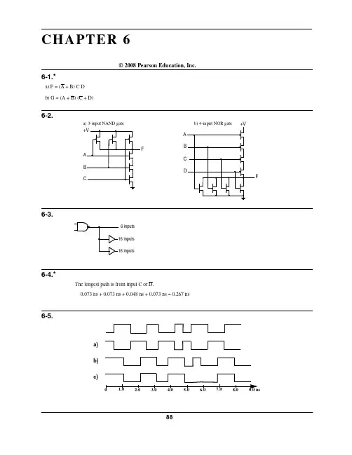
CHAPTER 6© 2008 Pearson Education, Inc.6-1.*6-2.6-3.6-4.*6-5.a) F = (A + B) C Db) G = (A + B) (C + D)a) 3-input NAND gate 6 inputs 16 inputs 16 inputsThe longest path is from input C or D.0.073 ns + 0.073 ns + 0.048 ns + 0.073 ns = 0.267 nsa)b)c)4.03.02.01.06.05.08.07.09.0 ns6-6.6-7. 6-8.+If the rejection time for inertial delays is greater than the propagation delay, then an output change can occur before it can be predicted whether or not it is to occur due to the rejection time.For example, with a delay of 2 ns and a rejection time of 3 ns, for a 2.5 ns pulse, the initialedge will have already appeared at the output before the 3 ns has elapsed at which whether to reject or not is to be determined.a) The propagation delay is t pd = max(t PHL = 0.05, t PLH = 0.10) = 0.10 ns.Assuming that the gate is an inverter, for a positive output pulse, the following actually occurs:If the input pulse is narrower than 0.05 ns, no output pulse occurs so the rejection time is 0.05 ns. The resulting model predicts the following results, which differ from the actual delay behavior, but models the rejection behavior: :0.10 ns0.05 ns0.10 ns0.10 ns6-9. 6-10.*b) For a negative output pulse, the following actually occurs:The model predicts the following results, which differs from the actual delay behavior andthe actual rejection behavior:Overall, the model is inaccurate for both cases a and b, and provides a faulty rejectionmodel for case b. Using an average of t PHL and t PLH for t pd would improve the delayaccuracy of the model for circuit applications, but the rejection model still fails.0.10 ns0.05 ns0.15 ns0.10 ns0.10 nsa)There is a setup time violation at 28 ns. There is an inputb)There is a setup time violation just before 24 ns, There is an inputc)There is a setup time violation at 28ns.d)There is a hold time violation at 16ns and a setup time violation at 24ns.combination violation around 24 ns.combination violation around 24 ns.a) The longest direct path delay is from input X through the two XOR gates to the output Y.t delay = t pdXOR + t pdXOR = 0.20 + 0.20 = 0.40 nsb) The longest path from an external input to a positive clock edge is from input X through the XOR gate and the inverter to the B Flip-flop.t delay = t pdXOR + t pd INV + t sFF = 0.20 + 0.05 + 0.1 = 0.35 nsc) The longest path delay from the positive clock edge is from Flip-flop A through the two XOR gates to the output Y.t delay = t pdFF + 2 t pdXOR = 0.40 + 2(0.20) = 0.80 nsd) The longest path delay from positive clock edge to positive clock edge is from clock on Flip-flop A through t delay-clock edge to clock edge = t pdFF + t pdXOR + t pdINV + t sFF = 0.40 + 0.20 + 0.05 + 0.10 = 0.75 nse) The maximum frequency is 1/t delay- clock edge to clock edge. For this circuit, t delay-clock edge to clock edgeis 0.75 ns, so the maximum frequency is 1/0.75 ns = 1.33 GHz.the XOR gate and inverter to clock on Flip-flop B.into its environment. Calculation of this frequency cannot be performed in this case since data for paths through the environment is not provided.Comment: The clock frequency may need to be lower due to other delay paths that pass outside of the circuit6-11.6-12.a) The longest direct path delay is from input X through the four XOR gates to the output Y.t delay = 4 t pdXOR = 4(0.20) = 0.80 nsb) The longest path from an external input to a positive clock edge is from input X through three XOR gates and the inverter to the clock of the second B Flip-flop.t delay = 3 t pdXOR + t pd INV + t sFF = 3(0.20) + 0.5 + 0.1 = 0.75 nsc) The longest path delay from the positive clock edge is from the first Flip-flop A through the four XOR gates to the output Y.t delay = t pdFF + 4 t pdXORR = 0.40 + 4(0.20) = 1.2 nsd) The longest path delay from positive clock edge to positive clock edge is from the first Flip-flop A through three XOR gates and one inverter to the clock of the second Flip-flop B.t delay-clock edge to clock edge = t pdFF + 3 t pdXOR + t pdINV + t sFF = 0.40+ 3(0.20) + 0.5 + 0.1 = 1.15 nse) The maximum frequency is 1/t delay-clock edge to clock edge. For this circuit, the delay is 1.15 nsso the maximum frequency is 1/1.15 ns = 870 MHz.Comment: The clock frequency may need to be lower due to other delay paths that pass outside of the circuit into its environment. Calculation of this frequency cannot be performed in this case since data for paths through the environment is not provided.AA6-13.*(Errata: Change "32 X 8" to "64 X 8" ROM)6-14. 6-15.6-16.IN OUT IN OUT IN OUT IN OUT 0000000000 00000100000001 01101000000011 00101100000100 1000 0000010000 00010100010001 01111000010011 00111100010100 1001 0000100000 00100100100001 10001000100011 01001100100101 0000 0000110000 00110100110001 10011000110011 01011100110101 0001 0001000000 01000101000010 00001001000011 01101101000101 0010 0001010000 01010101010010 00011001010011 01111101010101 0011 0001100000 01100101100010 00101001100011 10001101100101 0100 0001110000 01110101110010 00111001110011 10011101110101 0101 0010000000 10000110000010 01001010000100 00001110000101 0110 0010010000 10010110010010 01011010010100 00011110010101 0111 0010100001 00000110100010 01101010100100 00101110100101 1000 0010110001 00010110110010 01111010110100 00111110110101 1001 0011000001 00100111000010 10001011000100 01001111000110 0000 0011010001 00110111010010 10011011010100 01011111010110 0001 0011100001 01000111100011 00001011100100 01101111100110 0010 0011110001 01010111110011 00011011110100 01111111110110 0011a)16 + 16 + 1 = 33 address bits and 16 + 1 = 17 output bits, 8G × 17b)8 + 8 + 1 + 1 = 18 address bits and 8 + 1 = 9 output bitsc) 4 × 4 = 16 address bits and 14 output bits are needed, 64K × 14XYZXYZXYZXYZA B C D1111111111111111B = XY + XY + YZC = YZ C = YZ + Z A = XY + XY + YZBy using A instead of A and YZ instead of Y in D, YZ can be shared by all four functions. Further, since A is the complement of B, terms XY and XY can be shared between A and B. Thus, only four product terms YZ, XY, XY, and Z are required.An inversion must be programmed for A.6-17.6-18.6-19.*XY ZXYZ X YZ XY Z XYZ111111111X YZ 11AB CDEF11A = XYB = X + YZC = XY + X Y + ZD = YZE = 0F = ZImplementation of A, D, and E requires only two terms, XY and YZ. Straightforward implementation of B, C, and F requires four terms, XY , XYZ, XYZ, and Z. By implementing B, C, and F, only three additional termsX, X Y , and Z are required. So we form the solution using five product terms: XY , YZ, X Y, X, and Z. The solution is described by the equations given with the six K-maps.ABC D A BC D A BC D A BC D W X Y Z The values given in the four K-maps come from Table 3-1 on page 99.100110001100001111110000110011001111100d d d d dd d d d d dd d d d ddd d d d d dd W = A B + BC DX = BC D + BC + BD Y = CD + C D Z = D In this case, shared terms are limited. One such term B C D is generated in W.Assume 3-input OR gates.ABC DABC D ABCD ABC D W 100110001100001111110000110011001111100d d d d dd d d d ddd d d d ddd d d d d dd W = A + BC + BDX = BC D + BC + BD Y= CD + C D Z = D Each of the equations above is implemented using one 3-input OR gate. Four gates are used.6-20.6-21.X Y ZXYZX YZX Y Z11111111A B CD1A = XZ + YZ + X YZ B = XY + YZ + X YC = A + XYD = XY + Z1111111111Figure 6-23 uses 3-input OR gates.A, B, and D each require three or fewer product terms so can be implemented with 3-input OR gates.C requires four terms so cannot be implemented with a 3-input OR gate. But because the first PAL device outputcan used as an input to implement other functions it can be assigned to A and A can then be used to implement C using just two inputs of a 3-input OR gate.A ABCDABCD F111111111111111111GFigure 6-23 uses 3-input OR gates.Straightforward implementation of F requires five prime implicants and of G requires four prime implicants, but only 3 inputs are available on the PAL OR gates. So sum-of-products that can be factored from F and G or both and implemented by the other PAL cells are needed. A single sum of products that will work is H = ABC + BCD + BCD. The terms of H are shown with dotted lines on the K-maps. Using H:F = H + CD + ABG =H + AB There are other possible functions for H and corresponding results for F and H.。

数字电路与逻辑设计习题答案数字电路与逻辑设计习题答案数字电路与逻辑设计是计算机科学与工程领域中的重要基础课程,它涉及到数字信号的处理和转换,以及逻辑门电路的设计和分析。
学习这门课程时,习题是巩固知识和提高能力的重要途径。
下面将给出一些常见的数字电路与逻辑设计习题的答案,希望对大家的学习有所帮助。
1. 设计一个4位二进制加法器电路,实现两个4位二进制数的相加。
答案:一个4位二进制加法器电路可以由四个全加器电路组成。
每个全加器电路有三个输入:两个被加数和一个进位输入,以及两个输出:和位和进位输出。
将四个全加器电路按位级联,将进位输出连接到下一位的进位输入,最后一个全加器的进位输出作为最高位的进位输出。
和位的输出即为两个4位二进制数的和。
2. 给定一个3输入的逻辑电路,输出为1的条件是至少有两个输入为1。
请设计一个电路,实现这个逻辑功能。
答案:可以使用与门和或门组合的方式来实现这个逻辑功能。
首先,将三个输入分别与一个与门的三个输入相连,将输出连接到一个或门的输入。
然后,将三个输入分别与一个或门的三个输入相连,将输出连接到与门的输入。
这样,当至少有两个输入为1时,与门的输出为1,或门的输出也为1。
3. 给定一个4输入的逻辑电路,输出为1的条件是输入中有奇数个1。
请设计一个电路,实现这个逻辑功能。
答案:可以使用异或门实现这个逻辑功能。
首先,将四个输入两两分组,然后将每组的输出与另一组的输出进行异或操作。
最后,将四个异或门的输出连接到一个或门的输入。
这样,当输入中有奇数个1时,异或门的输出为1,或门的输出也为1。
4. 设计一个4位比较器电路,实现两个4位二进制数的大小比较。
答案:一个4位比较器电路可以由四个比较器组成。
每个比较器有两个输入:两个被比较的位,以及一个输出:比较结果。
将四个比较器电路按位级联,将每个比较器的输出连接到下一位比较器的输入。
最后一个比较器的输出即为两个4位二进制数的大小比较结果。
5. 给定一个3输入的逻辑电路,输出为1的条件是输入中的1的个数大于等于2。
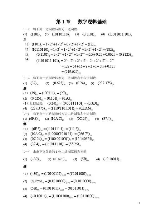
第1章 数字逻辑基础1-1 将下列二进制数转换为十进制数。
(1) 2(1101) (2) 2(10110110) (3) 2(0.1101) (4) 2(11011011.101) 解(1)3210210(1101)12120212(13)=⨯+⨯+⨯+⨯=(2)75421210(10110110)1212121212(182)=⨯+⨯+⨯+⨯+⨯= (3) 124210(0.1101)1212120.50.250.0625(0.8125)---=⨯+⨯+⨯=++=(4)76431013210(11011011.101)22222222 12864168210.50.125 (219.625)--=+++++++=+++++++= 1-2 将下列十进制数转换为二进制数和十六进制数(1) 10(39) (2) 10(0.625) (3) 10(0.24) (4) 10(237.375) 解(1)10216(39)(100111)(27)== (2) 10216(0.625)(0.101)(0.A)==(3)近似结果: 16210)3.0()00111101.0()24.0(D =≈ (4) 10216(237.375)(1110'1101.011)(0ED.6)== 1-3 将下列十六进制数转换为二进制数和十进制数(1) 16(6F.8) (2) 16(10A.C) (3) 16(0C.24) (4) 16(37.4) 解(1) 16210(6F.8)(1101111.1)(111.5)== (2) 16210(10A.C)(1'0000'1010.11)(266.75)== (3) 16210(0C.24)(1100.0010'01)(12.140625)== (4) 16210(37.4)(11'0111.01)(55.25)== 1-4 求出下列各数的8位二进制原码和补码(1) 10(39)- (2) 10(0.625) (3) 16(5B) (4) 2(0.10011)- 解(1)10(39)(1'0100111)(1'1011001)-==原码补码 (2) (0.1010000)(0.1010000)==10原码补码(0.625) (3) 16(5B)(01011011)(01011011)==原码补码(4) 2(0.10011)(1.1001100)(1.0110100)-==原码补码1-5 已知10X (92)=-,10Y (42)=,利用补码计算X +Y 和X -Y 的数值。

第1章计算机概述一、术语解释ENIAC: Electronic Numerical Integrator And ComputerALU: Arithmetic Logic UnitCU: Control UnitIC:Integrated CircuitULSI:Ultra Large Scale Integrated CircuitCPU: Central Processing UnitASCII: American Standard Code for Information InterchangeCAD:Computer-Aided DesignAI:Artificial Intelligence二、选择题1-5 ABACB 6-10 BBDDA 11-15 CADBD三、简答题1.计算机的特点是什么?(1)记忆能力强;(2)计算精度高与逻辑判断准确;(3)高速的处理能力;(4)能自动完成各种操作.2.计算机的发展经历了哪几代?各以什么器件为其主要特征?(1)电子管计算机(1946-1957)(2)晶体管计算机(1958-1964)(3)集成电路计算机(1965-1971)(4)大规模集成电路计算机(1972-现在)3.计算机有哪些方面的应用?请举例说明。
(1) 科学计算(2) 过程检测与控制(3) 信息管理(4) 计算机辅助系统(5) 人工智能4.什么是冯·诺依曼原理?(1)计算机应由运算器、控制器、存储器、输入设备和输出设备五个基本部件组成。
(2)内部以二进制表示指令和数据。
每条指令由操作码和地址码两部分组成。
操作码指出操作类型,地址码指出操作数的地址。
由一串指令组成程序。
(3)采用“存储程序”工作方式。
5.简述计算机的五大部件及其功能。
存储器不仅能存放数据,而且也能存放指令,形式上两者没有区别,但计算机应能区分数据还是指令;控制器应能自动执行指令;运算器应能进行加、减、乘、除四种基本算术运算,并且也能进行一些逻辑运算和附加运算;操作人员可以通过输入设备、输出设备和主机进行通信。
()7. short,int都是C++语言的关键字。
()8. C++编译系统对源程序编译时,可以检查出注释语句中的语法错误。
()9. 将一个字符常量放到一个字符变量中,并不是把该字符本身放到内存变量中去,而是将该字符相应的ASCII代码放到存储单元中。
()10. 语句int answer=3+2 9/(10-6);执行完毕后,变量answer的值是7.5。
三、单项选择题1. C++源程序文件的扩展名为()。
(A).CPP(B).OBJ(C).C(D).EXE2. 下列变量名中,()是合法的。
(A)double(B)A+a(C)CHINA(D)5s3. 下列符号能用作C++标识符的是()(A)xyz/2 (B)2xsale (C)x-sale (D)x_sale4. 下列各运算符中,()只能用于整型数据的运算。
(A)+(B)/(C) (D)%5.()不是C++的基本数据类型。
(A)字符类型(B)数组类型(C)整数类型(D)布尔类型6. 下列运算符中,优先级最高的是()。
(A)%(B)!(C)>=(D)/7. 字符串常量“ME”的字符个数是()。
(A)4(B)3(C)2(D)18. 在C++语言中,080是()。
(A)八进制数(B)十进制数(C)十六进制数(D)非法数9. 整型变量i定义后赋初值的结果是()。
int i=2.8 6;(A)12(B)16(C)17(D)1810.如有int m=31;则表达式(m++*1/2)的值是()。
(A)0 (B)15 (C)15.5 (D)1611.每个C++程序都必须有且仅有一个()。
(A)预处理命令(B)主函数(C)函数(D)语句12.在C++语言中,自定义的标志符()。
(A)能使用关键字并且不区分大小写(B)不能使用关键字并且不区分大小写(C)能使用关键字并且区分大小写(D)不能使用关键字并且区分大小写13.下列C++标点符号中表示一条语句结束的是()。
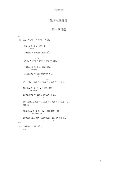
数字电路答案2210 = 2*81+ 6*8 0 = 268268 = 2 6 = 1011Q010110101102 = 00010110= 1^62 1 010810 = 1*8 + 5*8 + 4*8 = 15481548 = 1 5 4 = 11011002001101100110110Q = 0110(100= 6C 166 C1 0 - 113.12510 = 1*8 1 + 5*8 0 + 1*8 1 = 15.1815.18= 1 5. 1 = 1101.0012001 101 0011101.001 = 1101.0010= D.216D2131.62510 = 2*8 2 + 0*8 1 + 3*8 0 + 5*8 "1 =203.58203.58 = 2 0 3. 5= 10000011.101010 000 011 10110000011.10!= 10000011.1010= 83.A 1683A1-1数字电路答案 第一章习题(1) 1-2 (1)1011012= 101101= 5581011012= 0010(10仁2D558= 5*8 1 + 5*8 0 = 451011100101= 011{0010仁3451110010!= {1100101= E^6E 53458 = 3*8 2 + 4*8 1 + 5*8 0 = 22910(1)168 = 1*8 1+ 6*8 0= 1410168= 16= 1110200111011102= 1110= E 161728 二 1*8 2+ 7*8 1+ 2*8 01728 = 1 7 2 = 11110102001111 01011110102 01111010 7A 167 A61.538 = 6*8 1 + 1*8 0 + 5*8 1 + 3*8 2 = 49.6721。
61.538 = 6 1.5 3 = 110001.101011110 001 101 011110001.101011 = 00110001.10101100= 31.AC 1631A C2 10 1126.748 = 1*8 + 2*8 + 6*8 + 7*8 " 126.748 = 1 2 6. 7 4 = 1010110.1111001 010110 1111001010110.1111= 01010110.1111= 56.F 165 6 F1-41-3 101.0011= 101.001100= 5.148101.001!= 0101.0011= 5.3165.148 = 5*8 0 + 1*8"1+ 4*8 ■2 = 5.187510100111.101 = 100{11.{01=47.4100111.101 = 00100111.{010= 27.A 16 47.58 4*81 7*80 5*8 139.625i 0(1)-2+ 4*8 = 86.9375102A= 2 A = 101010,16001010101010102 = 101010= 528I 5 I 21 0528= 5*8 + 2*8 = 4210(1)(2)B2F16 = B 2 F = 1011001011111011 00101111101100101111 = 101100{l01f1仁545785 4 5 754578 = 5*8 3 + 4*8 2 + 5*8 1 + 7*8 0 = 2863。
3-1 分析题图3-1所示电路,写出电路输出Y 1和Y 2的逻辑函数表达式,列出真值表,说明它的逻辑功能。
解:由题图3-1从输入信号出发,写出输出Y 1和Y 2的逻辑函数表达式为1Y A B C =⊕⊕ ; 2()()Y A B C AB A B C A =⊕⋅⋅=⊕⋅+B将上式中的A 、 B 、C 取值000~111,分别求出Y 1和Y 2,可得出真值表如题解 表3-1所示。
题解 表3-1ABCA B ⊕()A B C ⊕⋅AB1Y2Y0 0 0 0 0 0 0 0 0 0 1 0 0 0 1 0 0 1 0 1 0 0 1 0 0 1 1 1 1 0 0 1 1 0 0 1 0 0 1 0 1 0 1 1 1 0 0 1 1 1 0 0 0 1 0 1 111111综上,由题解 表3-1可以看出,该电路实现了一位全加器的功能。
其中,A 和B 分别是被加数及加数,C 为相邻低位来的进位数;Y1为本位和数,Y 2为相邻高位的进位数。
3-2 分析题图3-2所示电路,要求:写出输出逻辑函数表达式,列出真值表,画出卡诺图,并总结电路功能。
解:由题图3-2从输入信号出发,写出输出F 的逻辑函数表达式为()()F A B C D =:::将上式中的A 、 B 、C 、D 取值0000~1111,求出F ,可得真值表和卡诺图分别如题解 表3-2和题解 图3-1所示。
题解 表3-2A B C DA B : C D :F0 0 0 0 1 1 1 0 0 0 1 1 0 0 0 0 1 0 1 0 0 0 0 1 1 1 1 1 0 1 0 0 0 1 0 0 1 0 1 0 0 1 0 1 1 0 0 0 1 0 1 1 1 0 1 0 1 0 0 0 0 1 0 1 0 0 1 0 0 11 0 1 0 0 0 1 1 0 1 1 0 1 0 1 1 0 0 1 1 1 1 1 0 1 1 0 0 1 1 1 0 1 0 0 1 1 1 1 1 1 1综上,由题解 表3-2可以看出,当输入A 、 B 、C 、D 中含有偶数个“1”时,输出;否则,当输入A 、 B 、C 、D 中含有奇数个“1”时,输出。
数字逻辑参考答案数字逻辑参考答案数字逻辑是计算机科学中的一个重要分支,它研究的是数字信号和数字电路的设计与实现。
在数字逻辑中,我们常常需要解决各种逻辑问题,包括逻辑运算、逻辑门电路的设计和分析等。
本文将为大家提供一些常见数字逻辑问题的参考答案,希望能对大家的学习和研究有所帮助。
1. 逻辑运算逻辑运算是数字逻辑中最基础的概念之一。
常见的逻辑运算包括与运算、或运算、非运算等。
下面是一些逻辑运算的参考答案:- 与运算(AND):输入A和B,输出为A与B的逻辑与结果。
逻辑表达式为:C = A AND B。
- 或运算(OR):输入A和B,输出为A与B的逻辑或结果。
逻辑表达式为:C = A OR B。
- 非运算(NOT):输入A,输出为A的逻辑非结果。
逻辑表达式为:B = NOT A。
2. 逻辑门电路逻辑门电路是数字逻辑中常见的电路实现方式,可以用于实现各种逻辑功能。
常见的逻辑门包括与门、或门、非门等。
下面是一些逻辑门电路的参考答案:- 与门(AND Gate):输入A和B,输出为A与B的逻辑与结果。
逻辑表达式为:C = A AND B。
可以使用两个晶体管和一个电阻来实现与门电路。
- 或门(OR Gate):输入A和B,输出为A与B的逻辑或结果。
逻辑表达式为:C = A OR B。
可以使用两个晶体管和一个电阻来实现或门电路。
- 非门(NOT Gate):输入A,输出为A的逻辑非结果。
逻辑表达式为:B = NOT A。
可以使用一个晶体管和一个电阻来实现非门电路。
3. 布尔代数布尔代数是数字逻辑中的一种代数系统,它由三个基本运算符(与、或、非)和一些基本规则组成。
布尔代数可以用来描述和分析逻辑运算和逻辑门电路。
下面是一些布尔代数的参考答案:- 分配律:对于任意的A、B和C,有A AND (B OR C) = (A AND B) OR (A AND C) 和 A OR (B AND C) = (A OR B) AND (A OR C)。
1CHAPTER 1© 2016 Pearson Education, Inc.1-1.(a)(1) Calm:(2) 10 mph(3) 100 mphor(b) The microcomputer requires a table or equation for converting from rotations/second to miles/hour. The pulses produced by the rotating disk must be counted over a known period of time, and the table or equation used to convert the binary count to miles per hour.1-2.–34° quantizes to –30° => 1 V => 0001+31° quantizes to +30° => 7 V => 0111 +77° quantizes to +80° => 12 V => 1100 +108° quantizes to +110° => 15 V => 11111-3.*Decimal, Binary, Octal and Hexadecimal Numbers from (16)to (31)1-4.1020301281282131,0723232233,554,4328828,589,934,592=⨯==⨯==⨯=K Bits M Bits G Bits21-5.220 = (1,000,00010 + d ) where d = 48,576 1Tb = 240 = (220)2 = (1,000,000 + d )2= (1,000,000)2 + 2(1,000,000) d + d 2 = 1,000,000,000,000 + 97,152,000,000 + 2,359,627,776 = 1,099,511,627,7761-6.112511212047252133,554,4311 Bits 1 Bits ⇒-=⇒-=1-7.*63202641013275321142(1001101)222277(1010011.101)22222283.625(10101110.1001)2222222174.5625----=+++==+++++==++++++=1-8.1 1 0 0 0 0 0 0 0 0 0 1 0 11-9.*1-10.*a)0.45 × 8 = 3.6 =>0.60 × 8 = 4.8 =>0.80 × 8 = 6.4 =>0.20 × 8 = 3.2 =>10= (16612.3463)8b) (1938.257)10 = (792.41CB)16c) (175.175)10 = (10101111.001011)21-11.*a) (673.6)8= (110 111 011.110)2= (1BB.C)16b) (E7C.B)16= (1110 0111 1100.1011)2= (7174.54)8c) (310.2)4= (11 01 00.10)2= (64.4)81-12.a) 1010 b) 0110 c) 1111001×1100 ×1001 ×0111010000 0110 11110010000 0000 0000001010 0000 11110011010 0110 11110011111000 0110110 11110010000000110110110101341-13.+1000110110101101010000000010000110001101011-----Quotient = 10001R emainder = 1 1-14.(a) 6 × 123 + 8 × 122 + 7 × 121 + 4 = 11608 (b)12 1-15.a)0 1 2 3 4 5 6 7 8 9 A BCDEFGHIJb) 20c) 21012010(.)1120122018201620(4658.8)BCI G -=⨯+⨯+⨯+⨯=1-16.*a) (BEE)r = (2699)1021021114142699111426850r r r r r ⨯+⨯+⨯=⨯+⨯-=By the quadratic equation: r = 15 or ≈ –16.27 ANSWER: r = 15 b) (365)r = (194)102102365194361890r r r r r ⨯+⨯+⨯=⨯+⨯-=By the quadratic equation: r = – 9 or 7 ANSWER: r = 751-17.Errata: The text has an error: 1480 should be 1460. This will be corrected in future printings.Noting the order of operations, first add (34)r and (24)r101010(34)34(24)24(34)(24)58r r r r r r r r r r =⨯+⨯=⨯+⨯+=⨯+⨯Now, multiply the result by (21)r101021(21)(58)10218⨯+⨯⨯⨯+⨯=⨯+⨯+r r r r r r Next, set the result equal to (1480)r and reorganize.21321321010218146161580⨯+⨯+=⨯+⨯+⨯⨯-⨯-⨯-⨯=r r r r r r r r r Finally, find the roots of this cubic polynomial. Solutions are: r = 8, – 1, – 1ANSWER: The chicken has 4 toes on each foot (half of 8).1-18.*a) (0100 1000 0110 0111)BCD = (4867)10= (1001100000011)2 b) (0011 0111 1000.0111 0101)BCD= (378.75)10=(101111010.11)21-19.*(694)10 = (0110 1001 0100)BCD (835)10=(1000 0011 0101)BCD1001 0100 +0011 +0101 1100 1001 +0110 +00001 001010011-20.*(a)101 1000111 1000Move R 011 1100 0 100 column > 0111Subtract 3 −0011011 1001 0Subtract 3 −001101 1001Move R 0 1100 110 100 column > 0111Subtract 3 −00110 1001 110Move R 0100 1110Move R 010 01110Move R 01 001110Move R 0 1001110 Leftmost 1 in BCD numbershifted out: Finished(b) 102101 1000011 1001 0111Move R 001 1100 1011 1 101 and 100 columns > 0111Subtract 3 −0011 -0011001 1001 1000 1Move R 00 1100 1100 01 101 and 100 columns > 0111Subtract 3 −0011 −001100 1001 1001 01Move R 0 0100 1100 101 100 column > 0111Subtract 3 −00110 0100 1001Move R 0010 0100 1101Move R 001 0010 01101Move R 00 1001 001101 100 column > 0111Subtract 3 −001100 0110 001101Move R 0 0011 0001101Move R 0001 10001101Move R 000 110001101 Leftmost 1 in BCDnumber shifted out: Finished 1-21.(a) 10210110011110001st Move L 1 1110002nd Move L 11 110003rd Move L 111 1000 100 column > 100Add 3 00111010 10004th Move L 1 0101 000 100 column > 100Add 3 00111 1000 0005th Move L 11 0000 006th Move L 110 00000 101 column > 100Add 3 00111001 0000 07th Move L 1 0001 00000 Least significant bit in binary number moved in:Finished(b) 103102101100011100101111st Move L 0 11100101112nd Move L 01 1100101113rd Move L 011 100101114th Move L 0111 0010111 100 column > 100Add 3 001161010 00101115th Move L 1 0100 0101116th Move L 10 1000 10111 100 column > 100Add 3 001110 1011 101117th Move L 101 0111 0111 101 & 100 columns > 100Add 3 0011 00111000 1010 01118th Move L 1 0001 0100 1119th Move L 10 0010 1001 11 100 column > 100Add 3 001110 0010 1100 1110th Move L 100 0101 1001 1 101 &100 columns > 100Add 3 0011 0011100 1000 1100 111th Move L 1001 0001 1001 Least significant bit in binary number moved in: Finished1-22.From Table 1-5, complementing the bit B6 will switch an uppercase letter to a lower case letter and vice versa.1-23.a) The name used is Brent M. Ledvina. An alternative answer: use both upper and lower case letters.0100 0010 B 0101 0010 R 0100 0101 E0100 1110 N 0101 0100 T 0010 0000 (SP)0100 1101 M 0010 1110 . 0010 0000 (SP)0100 1100 L 0100 0101 E 0100 0100 D0101 0110 V 0100 1001 I 0100 1110 N0100 0001 Ab) 0100 0010 1101 0010 1100 01010100 1110 1101 0100 1010 00000100 1101 0010 1110 1010 00001100 1100 1100 0101 0100 01000101 0110 1100 1001 0100 11100100 00011-24.1000111 G1101111 o01000001000011 C1100001 a1110010 r1100100 d1101001 i1101110 n1100001 a (Errata: This number appears as 110001, which would be “1”)1101100 l1110011 s0100001 !781-25.*a) (11111111)2b) (0010 0101 0101)BCD c) 011 0010 011 0101 011 0101ASCIId)0011 00101011 01011011 0101ASCII with Odd Parity1-26.a) U+0040 = 01000000b) U+00A2 = 11000010 10100010c) U+20AC = 11100010 10000010 10101100d)U+1F6B2 = 11110000 10011111 10011010 101100101-27.Binary Numbers from (32)to (47) with Odd and Even Parity1-28.Gray Code for Hexadecimal Digits1-29.(a) Wind Direction Gray CodeDirectionCode WordN 000 S 110 E 011 W 101 NW 100 NE 001 SW 111 SE0109(b) Wind Direction Gray Code (directions in adjacent order)DirectionCode WordN 000 NE 001 E 011 SE 010 S 110 SW 111 W 101 NW100As the wind direction changes, the codes change in the order of the rows of this table, as suming that the bottom row is “next to” the top row. From the table, the codes that result due to a wind direction change always change in a single bit.1-30.+The percentage of power consumed by the Gray code counter compared to a binary code counter equals:Number of bit changes using Gray code Number of bit changes using binary codeAs shown in Table 1-6, and by definition, the number of bit changes per cycle of an n-bit Gray code counter is 1 per count = 2n .Number of bit changes using Gray code = 2nFor a binary counter, notice that the least significant bit changes on every increment. The second least significant bit changes on every other increment. The third digit changes on every fourth increment of the counter, and so on. As shown in Table 1-6, the most significant digit changes twice per cycle of the binary counter.Number of bit changes using binary code 11222n n -+++(1)110221(21)122nni i n n i i ++==⎡⎤==-=--=-⎢⎥⎣⎦∑∑ % Power (1)210022n n +=⨯-。
浙江大学计算机学院实验教学中心逻辑与计算机设计基础实验2010~2011秋冬9掌握二进制计数器/定时器的工作原理与设计方法掌握用计数器进行分频的概念和方法实验设备装有ISE的计算机系统1台Spartan III 实验板1套实验材料无设计一个数字钟,使用60进制和24(12)进制计数器,实现24小时内时间的实时显示。
60进制计数器用10进制与6进制计数器的组合来实现;24(12)进制可用类似方法实现。
采用4个计数器分别实现分钟的个位、分钟的十位、小时的个位、小时的十位计数。
数字钟的初值通过初始化语句来实现,用数码管前两位显示小时的十位和个位,后两位显示分钟的十位和个位。
把时钟加到多功能计算器中。
计数器是复杂数字系统和计算机硬件系统中的一个基本部件,是计数、分频、定时、同步和时基等电路的核心,在计算机、网络、通信等设备中经常使用到。
本实验以计数器为例,采用行为级描述的方法设计时序电路,实现各种常用的计数器和定时器。
•60进制计数器用10进制与6进制计数器的组合来实现•24进制计数器用4进制与6进制计数器的组合来实现module m_gen_min (clk_sec, clk_hour, min_low, min_high);input wire clk_sec;output reg clk_hour;output reg [3:0] min_low, min_high;reg [15:0] cnt;always @(posedge clk_sec) begin if (clk_hour == 1)clk_hour = 0;if (cnt == 59) begin cnt = 0;if (min_low == 9) begin min_low = 0; /* base 10 */if (min_high == 5) begin min_high = 0; /* base 6*/clk_hour = 1;end else min_high = min_high + 1;end else min_low = min_low + 1;end else cnt = cnt + 1;endendmodule分钟的生成以秒脉冲为时钟信号,将10进制和6进制组合成60进制,并产生小时脉冲信号。
《程序设计基础》实验教程对于从事计算机行业的人员来说,设计能力是最主要的基本功之一。
入门课程《程序设计基础》的学习效果将直接关系到编程能力的掌握和提高以及后续课程的学习。
然而,实践证明,许多初学者在学习这门课程时的效果并不理想。
对初学者来说,如何学好本课程?首先,要理解教材中所给出的语法描述,并学会按语法规定去编写指定问题的求解程序。
经过这样的多次反复,初学者就可以找到编程的感觉。
除了要学好理论知识外,更重要的一点是要到计算机上去验证,因为只有实践才是检验真理的标准。
只有通过到计算机上去实践,才能发现学习中存在的问题,巩固所学知识,加强解决实际问题的能力,增强信心。
因此,《程序设计基础》课程的上机实验是本课程必不可少的实践环节,必须加以重视。
本课程上机实验的目的是使学生熟悉用高级语言解决实际问题的全过程,加深对语言的理解,得到程序设计基本方法和能力的训练。
在独立编写程序、独立上机调试程序的同时,真正能用高级语言这个工具去解决实际问题,对计算机学科的相关知识有所了解,从而为后续课程的学习奠定良好的基础。
本实验指导所用环境是Visual C++ 6.0及以上版本。
考虑到本课程的内容和特点,设置了十四个实验,每次实验需要两至三小时,分别侧重于教材中的一个方面,其中标有“*”号的习题的综合性较强,可供学有余力的学生选择。
实验时也可根据具体情况做适当调整。
虽然可能由于课时和机时限制等原因而不能在实验课时内全部得到安排,但还是建议学生能将其中的每个实验都能认真做一遍,因为这些实验都是学习本课程所必需的。
学生在做实验之前应仔细阅读本实验指导书,初步掌握实验的基本要求和实验方法。
在实验过程中,学生应该有意识的培养自己调试程序的能力,积累发现问题、解决问题的经验,灵活主动的学习。
对于分析运行结果的实验习题,上机前先进行用人工分析,写出运行结果,与上机调试得到的结果进行对照,如有差异,分析其原因。
对于程序编制的实验习题,上机前应考虑出较成熟的编程思路,有意识提供出多种方案,以灵活运用所学知识和技巧。
第二章布置习题参考解
2-1 用真值表验证XYZ=X+Y+Z 三变量DeMorgan定律
2-2 用代数化简来证明下列布尔方程的性质
a)
c)
2-3 用代数化简来证明下列布尔方程的性质
2-6 化简下列布尔表达式,使表达式中包含的因子最少
2-10
a)
c)
2-11
2-12
2-13
2-14
2-15
2-16
2-19
2-24
(a) 用两个三态缓冲器和一个非门实现函数H=XY+XZ。
(b) 用两个缓冲器和两个非门互联实现异或门。
2-33
(a) 把三个三态缓冲器的输出连在一起,增加一些逻辑(门)实现函数F=ABC+ABD+ABD C、D以及D是三态缓冲器的输入,A、B通过逻辑电路产生使能输入。
(b) 对于(a) 中设计的三态缓冲器的输出是不是没有冲突?如果不是,更改必要的设计,使设计的电路没有冲突。
上述设计没有三态输出冲突。
第二章布置习题参考解
2-1 用真值表验证定律2-2 用代数化简来证明下列布尔议程的性质
a)
c)
2-3 用代数化简来证明下列布尔议程的性质
2-6 化简下列布尔表达式,使表达式中包含的因子最少
2-10
a)
c)
2-11
2-12
2-13
2-14
2-15
2-16
2-19
2-21
2-24
(a)
用两个三态缓冲器和一个非门实现函数H=XY+XZ。
把两个缓冲器和两个非门互联实现异或门。
(b)
2-33
把三个三态缓冲器的输出连在一起,增加一些逻辑(门)实现函数 (a)
F=ABC+ABD+ABD。
假设C、D以及D是三态缓冲器的输入,A、B通过逻辑电路产生便能输入。
对于(a) 中设计的三态缓冲器的输出是不是没有冲突?如果不是,更改必 (b)
要的设计,使设计的电路没有冲突。
上述设计没有三态输出冲突。