cadence入门教程
- 格式:pdf
- 大小:2.32 MB
- 文档页数:41
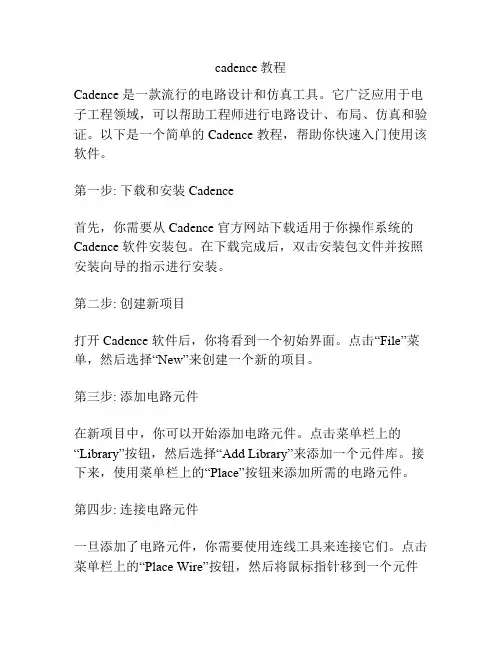
cadence教程Cadence 是一款流行的电路设计和仿真工具。
它广泛应用于电子工程领域,可以帮助工程师进行电路设计、布局、仿真和验证。
以下是一个简单的 Cadence 教程,帮助你快速入门使用该软件。
第一步: 下载和安装 Cadence首先,你需要从 Cadence 官方网站下载适用于你操作系统的Cadence 软件安装包。
在下载完成后,双击安装包文件并按照安装向导的指示进行安装。
第二步: 创建新项目打开 Cadence 软件后,你将看到一个初始界面。
点击“File”菜单,然后选择“New”来创建一个新的项目。
第三步: 添加电路元件在新项目中,你可以开始添加电路元件。
点击菜单栏上的“Library”按钮,然后选择“Add Library”来添加一个元件库。
接下来,使用菜单栏上的“Place”按钮来添加所需的电路元件。
第四步: 连接电路元件一旦添加了电路元件,你需要使用连线工具来连接它们。
点击菜单栏上的“Place Wire”按钮,然后将鼠标指针移到一个元件的引脚上。
点击引脚,然后按照电路的设计布局开始连接其他元件。
第五步: 设置仿真参数在完成电路布局后,你需要设置仿真参数。
点击菜单栏上的“Simulate”按钮,然后选择“Configure”来设置仿真器类型、仿真时间等参数。
第六步: 运行仿真设置完成后,你可以点击菜单栏上的“Simulate”按钮,然后选择“Run”来运行仿真。
仿真过程会模拟电路的运行情况,并生成相应的结果。
总结通过这个简单的 Cadence 教程,你了解了如何下载安装Cadence 软件、创建新项目、添加电路元件、连接元件、设置仿真参数和运行仿真。
掌握了这些基本操作后,你可以进一步学习和探索 Cadence 的更多功能和高级技巧。
祝你在使用Cadence 中取得成功!。
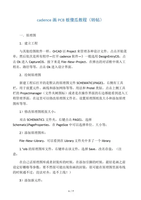
cadence画PCB板傻瓜教程(转帖)一.原理图1.建立工程与其他绘图软件一样,OrCAD以Project来管理各种设计文件。
点击开始菜单,然后依次是所有程序—打开cadence软件—》一般选用DesignEntryCIS,点击Ok进入CaptureCIS。
接下来是File--New--Project,在弹出的对话框中填入工程名、路径等等,点击Ok进入设计界面。
2.绘制原理图新建工程后打开的是默认的原理图文件SCHEMATIC1PAGE1,右侧有工具栏,用于放置元件、画线和添加网络等等,用法和Protel类似。
点击上侧工具栏的Projectmanager(文件夹树图标)或者是在操作界面的右边都能看到进入工程管理界面,在这里可以修改原理图文件名、设置原理图纸张大小和添加原理图库等等。
1)修改原理图纸张大小:双击SCHEMATIC1文件夹,右键点击PAGE1,选择Schematic1PageProperties,在PageSize中可以选择单位、大小等;2)添加原理图库:File--New--Library,可以看到在Library文件夹中多了一个library1."olb的原理图库文件,右键单击该文件,选择Save,改名存盘;(注意:在自己话原理图库或者封装库的时候,在添加引脚的时候,最好是画之前设定好栅格等参数,要不然很可能出现你画的封装,很可能在原理图里面布线的时候通不过,没法对齐,连不上线!)3)添加新元件:常用的元件用自带的(比如说电阻、电容的),很多时候都要自己做元件,或者用别人做好的元件。
右键单击刚才新建的olb库文件,选NewPart,或是NewPartFromSpreadsheet,后者以表格的方式建立新元件,对于画管脚特多的芯片元件非常合适,可以直接从芯片Datasheet中的引脚描述表格中直接拷贝、粘贴即可(pdf格式的Datasheet按住Alt键可以按列选择),可以批量添加管脚,方便快捷。
Cadense15.5.1 Design Entry CIS 入门的入门教程(北京索为高科系统技术有限公司 雒海涛) 一、cadence15.5.1 安装 1、安装文件组成:四张光盘,我下载的这个版本四张光盘如下:第一张为【强大的电子设计系统 Cadence.SPB.15.5.1].zwtspb15.bin】其他三场看最名称 最后一个字母 b c d 就是顺序了。
2、安装 cadence 虚拟光驱打开第一张光盘, 里面有个 crack 破解拷贝出来, 不需要安装 license server, 直接安装 product 即可, 安装过程中需要输入的地方一概不需要输入, 一路 next 直到安 装完成。
将 拷 贝 出 来 的 license 文 件 放 到 一 个 合 适 的 位 置 ( 建 议 放 在 安 装 目 录 下 D:\Cadence\license\license.dat) 。
添加环境变量:LM_LICENSE_FILE=D:\Cadence\license\license.dat 3、修改文件 如果使用 cadence 的 project manager 模块,启动后 setup 的时候会出个错误,是路 一个路径错误问题,到 D:\Cadence\SPB_15.5.1\share\library 目录下找到 cds.lib 文件,用 记 事 本 打 开 , 修 改 里 面 的 第 九 行 DEFINE spiceelem ./spiceelem 改 为 DEFINE spice_elem ./spice_elem(spice_elem 这个文件夹可以在这个目录下找到) ,这样就好了。
二、启动 Design Entry CIS Cadence 安装完成后菜单如下: (发现什么没?这个软件肯定很大,恶笑中……..)选择 Design Entry CIS,接下来我们的原理图绘制就要在 Design Entry CIS 完成了。
Cadence TutorialI. IntroductionThis tutorial provides an introduction to analog circuit design and simulation with Cadence, and covers the features that are relevant for the homework assignments. The tutorial is divided into the following topics:•Logging on and Starting Cadence•Creating a Designo Creating a new library and cellviewo Placing the Partso Editing the Symbol Propertieso Wiring the Schematico Modifying Wire Attributes•Analyzing the Design and Plotting Resultso Finding the DC Operating Point and performing a DC Sweepo Performing a Transient Analysiso Performing an AC Analysiso Performing a Parametric Sweepo A Note on Measuring Currentso A Note on Plotting•Invoking Cadence Helpo Getting Additional Help with CadenceThroughout the document, the followingII. Logging on and Starting CadenceIn order to use the ECE164-provided installation of Cadence, you either need to be sitting at one of the Linux workstations provided for use by ECE264 students (see the ECE264 website for the locations of these workstations), or you can login remotely to . In either case, you should login with your Open Computing Environment account obtained via Academic Computing Services (ACS).If you wish to login remotely, you will need SSH and X-server software on your local machine. The necessary software is available as part of the operating systems on Sun Workstations, PCs running Linux, and Macintosh computers running OS X. It can be obtained via third parties for computers running Windows. Students who wish to login remotely are responsible for obtaining (if running Windows), learning how to use, and maintaining their own SSH and X-server software.Once you have logged in, open a terminal window if one does not open automatically and type the following in the window:ee264acd ece-cadenceicfb &A window containing text should appear at the bottom of the screen, labeled “icfb - ...”. This is sometimes called the CIW (Command Interpreter Window). A window explaining new features should also come up; in this window, select “Edit > Off at Startup”, and then close it. The CIW window is the main Cadence window, and much useful information is displayed here. If Cadence isn’t doing what you expect, it is often helpful to look here to read the error messages. You may find it helpful to enlarge the window.You now need to bring up the library manager. To do this, select “Tools > Library Manager” in the CIW. A “Library Manager” window appears. Notice the library “ece264lib”.This library contains most if not all of the IC components (e.g., transistors, resistors, etc.) that will be used in this class.II.Creating a DesignThe creation of a simple transistor amplifier is described in this section. The following notational conventions are used in the description:•The text “[LIB]” should be replaced with “164” if you are taking ECE164 and by “264” if you are taking ECE264.•Bracketed letters such as “[a]” denote keyboard shortcuts (bindkeys) which can be used instead of the menus or buttons to accomplish the given task. To use them, place the pointer over the appropriate window and simply press the key. Please note that these bindkeys are case sensitive.For letters enclosed by square brackets such as “[a]”, the pointer must be in a schematic window.For letters enclosed by curly brackets such as “{a}”, the pointer must be in a waveform window. A summary of the most useful bindkeys is listed in Appendix A.Creating a new library and cellview1.Create a new library named “tutorial”:(a)In the CIW, select “File > New > Library”, and a “New Library” windowwill appear.(b)In the “Name” field, enter “tutorial”.(c)Verify that the path (near the bottom of the dialog box) points to your working directory(or wherever you’d like to place all your class libraries). This path will by default pointto the directory from which you invoked Cadence(d)Select the “Don't need a techfile” button, then click “OK”. In the LibraryManager, an entry “tutorial” should appear.2.Create a new schematic cellview in our new library.(a)In the CIW, select “File > New > Cellview...”, and a “Create New File”dialog box appears.(b)Ensure that the “tutorial” is selected for Library Name (by clicking on the squarebutton).Type “tutorial” in the “Cell Name” field as well.(c) Type “schematic” in the “View Name” field.(d)Select “Composer - Schematic” in the “Tool” field if it is not already selected,then click “OK”. An empty schematic window appears.(e)In the schematic window, select “Design > Save”. You have now successfullycreated a cellview.Placing the PartsYou will now place symbols on the Schematic Window as shown in Figure 1.Figure 1: Initial parts placement.1.Find and place the pMOST symbol as follows:(a)With the schematic window active, press “i” on the keyboard. An “Add Instance”dialog box will appear. The “i” key is a bindkey, or shortcut key, to this dialog box.You can also get the same dialog box by click on the “Instance” button on the lefthand side of the schematic window (it looks like a little DIP), or by going to “Add >Instance” in the menu bar (there is an “i” next to this menu selection, notice). Thereare many shortcuts like this throughout Cadence, and you can create more if you wish -see the online help. Note also that at the bottom of the schematic window and the CIW,the instructions “Point at location for the instance” appears, along withinformation about what the mouse buttons do: “mouse L: ...”. It’s often importantto look at these messages to figure out what is going to happen when you press theleft/middle/right mouse buttons. The mouse buttons are bound to Skill functions, but canbe reconfigured - see the online help for more details.(b)In the dialog box Library field, enter “ece[LIB]lib”. For Cell, enter “pmos4”. ForView, enter “symbol”. You can also use the Browse button to invoke the LibraryBrowser to find a part.(c)When you move the mouse over the schematic window, you will see the outline of a 4-terminal pMOST. Move the cursor to the desired location and press the left mousebutton. Repeat for the other pMOST transistor.(d)To stop placing pMOST symbols, press “ESC” on the keyboard (with the SchematicWindow active), or click the “Cancel” button in the Add Instance dialog box.2.Place an nMOST using a similar procedure. This time, try using the Library Browser to place the“nmos4” symbol. Position it relative to the pMOST symbols as shown in Figure 1, then press “ESC” to get rid of the Add Instance window.3.Next, place the DC Current Source symbol as follows:(a)Press “i” as before, then click “Browse” to bring up the Library Browser.(b)Select “ece[LIB]lib” in the Browser library list, then find the “idc” componentsymbol using the scroll bar. Highlight this component in the browser by left-clicking on“idc”. Sometimes you may need to specify that you want to place the “symbol”version of this part.(c)Move the mouse over the schematic window and place it in the desired location. Don’tpress “ESC” yet.4.Go back to the Library Browser and find the “vdc” part. Place it.5.Similarly, place the “vsin”, “res”, and five copies of “gnd”. Finally, press “ESC” (remember,the Schematic Window must be active) to stop placing parts.6.If you need to move any of the parts, use the following procedure:(a)Press “M” (stretch) or “m” (move). Note the message at the bottom of the SchematicWindow. At this point, there is no difference between these two commands. But whenwires are attached to the parts, “M” will move the wires as well, whereas “m” will justmove the part.(b)Click on the part you wish to move. Again, keep an eye on the bottom of the SchematicWindow. Follow the instructions there. Repeat as needed.(c)Note that you can also move items by moving the cursor over the item, pressing andholding the left mouse button, moving the mouse, and then releasing the mouse button.Editing the Symbol PropertiesOnce all the parts are placed on the schematic, you can set property values that are specific to the design on each symbol. Figure 2 shows many of the property values that you will add in this part of the tutorial. The “vsin” symbol has many properties: “acm” is “AC Magnitude”, the amplitude of the AC signal applied to the linearized circuit (small signal circuit) during an AC Analysis. The “acp” is the “AC Phase”, “vo” refers to “DC Offset”, and “vm” refers to “Amplitude”, the amplitude of the signal applied to the large-signal (non-linear) circuit during a Transient Analysis.Figure 2: Symbol property values.e the following procedure to change a symbol’s properties. Before you begin, make sure thatyou have pressed ESC to clear the last action performed (the bottom line of the Schematic Window should read “>”):(a) Move the cursor to a location where there are no parts. Then press “q”. An “EditObject Properties” dialog box will appear.(b)Click on the item whose properties you’d like to change. The dialog box will expand todisplay a list of properties that can be changed. If you can’t see any properties, makesure thatthe “CDF” box is checked near the top of the “Edit Object Properties”window.(c)In the list of properties, edit those that you would like to change or specify. DO NOTinclude units such as “Volts” or “Ohms” - you’ll notice that these are filled inautomatically after you move on to the next property. DO NOT press return after youenter a property - use the mouse or use the “TAB” key to proceed. DO specifyabbreviations for scientific notation such as “k” (kilo),”u” (micro), “m” (milli), “M”(mega), “p” (pico), “f” (femto).(d)Click on the next part to change its properties. Cadence will ask whether you want tosave the property changes from the old part - say yes.(e)When you’re done entering properties, click “Cancel” at the top of the “EditObject Properties” dialog box.2. Change the names of the transistors according to Figure 2 by changing the “Instancename” field. Note: The name must be unique. Also insert the values for the transistor widthsand lengths.3.Flip the display of transistor M0 by first pressing “m” and clicking on the transistor to move it.While you are “holding” it, press “R” on the keyboard. The symbol outline should flip. Place theflipped part as shown in Figure 2.4.Note that the ac magnitude and phase of the “vsin” part are not displayed by default. Edit theproperties of this part (with the “q” key, and then look at the “AC Magnitude” property. Clickon the button to the right of the property value, and a list of choices will appear. Select “Both”.This will cause this property to be displayed on the schematic.Wiring the SchematicAfter the symbols are placed and the properties are set, you can wire the parts together as shownin Figure 3 by doing the following:1.One way to create a wire between two ports is as follows:(a)Position the mouse cursor over the first port (for example, start with the top of theconstant voltage source).(b)Click and hold the left mouse button.(c)Position the mouse cursor over the second port (the Vdd symbol above the Vdc symbol).(d)Release the left mouse button.(e)Repeat steps a through d to connect each Ground and Vdd symbol to the associatedparts, as shown in Figure 3.2. To connect the Gate terminals of the pMOSTs to the Drain terminal of M1, do the following:(a)Press “w” on the keyboard. Note the instructions at the bottom of the SchematicWindow.(b)Click and hold the left mouse button.(c)Position the cursor over the mid-point of the wire between the Gate terminals of M1 andM2, and click the left mouse button.(d)Move the mouse cursor four grid-points down, and click the left mouse button.(e)Move the mouse cursor six grid-points to the left, and click the left mouse button. Thiscompletes the connection.plete the remaining wire connections as shown in Figure 3.Figure 3: Schematic Wire Connections.Modifying Wire AttributesIf you do not label wires, Cadence automatically provides names for each wire, such as “net30”. It can be helpful later on during design and analysis if you label the wires with meaningful designators that are easy to understand and refer to. To add the attribute “vout” to the wire shown in Figure 3, do the following:1. Press “l” (for label) on the keyboard. An “Add Wire Name” dialog box appears.2.Enter “vout vin” in the “Names” field and press “Return”3.Move the cursor until the dot is on top of the wire to be labeled “vout”. Left click once with themouse. The label will be attached to the wire, and the label you are moving with your cursor changes.4.Place the “vin” label in an appropriate spot. Make sure the dot is on top of the wire before youleft-click.Finally, add a single instance of “ece[LIB]lib title” underneath your schematic. Please make sure that this is always placed in all your schematics.At this point you have a completed design that is ready to be analyzed. In the next part of the tutorial, you will simulate the amplifier. First, save the design by clicking the checkmark icon (the Check and Save icon) on the left hand side of the Schematic Window (top). Check the CIW. There should be a message saying that “Schematic Check completed with no errors”. Whenever you make a change to your design, you’ll need to check and save before you simulate. Otherwise, you may get an error, which will show up in the CIW window. Again, the CIW is extremely important for finding errors. You should read any errors carefully, and sometimes warnings are important too.III. Analyzing the DesignBefore performing the circuit analysis, you need to start the analog environment by going to “Tools > Analog Environment” in the schematic window. A new window called the“Simulation Window” will appear.Next you need to tell Cadence where to find the model library. For this class, we have a single model library file, called “cmos018.scs”, which contains an nMOST model named “N”, and a pMOST model named “P”. The symbols we’re using by default have these names specified in their symbol properties (look at the properties for one of the transistors). If you ever decide to use a different symbol, you’ll need to make sure the “Model name” property is correctly filled in. To tell Cadence where to look for the model file, go to “Setup > Model Libraries” in the Simulation Window. In the “Model Library File” field, enter:/home/linux/ieng6/ee164f/your_login_name/ece-cadence/cmos018.scs(if you are taking EE164)or/home/linux/ieng6/ee264a/your_login_name/ece-cadence/cmos018.scs(if you are taking EE264a)where “your_login_name” should be replaced by the name of the account under which you logged into the system (e.g., bobama). Then click on “Add” (NOT “OK”). You’ll see the path placed in the list of Model Library Files. Now click on “OK”.Finding the DC Operating Point and Performing a DC SweepIn this section, you’ll find and annotate the DC operating point, and you’ll sweep the input voltage to find the correct bias voltage for the nMOST transistor.1.Now go to “Analyses > Choose...”. A new dialog box will appear. [a]2.In the new dialog box, select the “dc” button. Check the “Save DC Operating Point” box.This will allow us to annotate node voltages later. Finally click “OK”3.We’ll now perform our first simulation. Click on the “Netlist and Run” icon, which is thegreen traffic light on the right hand side of the Simulation Window. If this is your first time running Cadence, a “Welcome” menu appears – close it. A new window will appear, hopefully saying that the simulation was successful, and providing a brief summary of the simulation convergence. [s]4.If everything went well, go to the Simulation Window, and select “Results > Annotate >DC Node Voltages”[d]. Note that the voltages at each terminal of each device are now marked on the schematic. Now go to “Results > Annotate > DC Operating Point”[D]. Note that important voltages and currents are now marked on each device. You can quicklysee whether the devices are biased properly. You can remove this annotation by using “Results > Annotate >Design Defaults”[^d].5.You should see a problem with the node voltages. The node “vout” should be about 2.4V. Thismeans that the top pMOST is operating in triode, and this amplifier will not work properly. You’ll now fix this using a DC sweep to find the correct bias point.6.Go back to the Simulation Window, and select “Analyses > Choose...” [a]. Under “SweepVariable” on the DC Analysis Form, select “Component Parameter”. The form will become larger.7.On the expanded form, click the “Select Component” button. You will be prompted to selecta component on the schematic. Select the “vsin” symbol at the nMOST input. A new window willappear, and you should select “dc” as the parameter you wish you vary, then click “OK” in the new window.8.Fill in the rest of the form so that the voltage is swept from 0 to 2.5V. Set the sweep type to“Linear”, and set the number of points to be plotted to 500. When you’re done, click “OK” on the Choose Analyses window.9.Now you need to select an output to plot. To plot a voltage, use the following procedure:10.Go to “Outputs > To Be Saved > Select on Schematic” in the SimulationWindow. Left-click on the “vout” and “vin” nets in the schematic window, and then press “ESC”. This step is typically not done as you can simply click on the nodes you want to plot after the simulation is complete. However, go ahead and try it this time.11.Go to “Outputs > Setup...”. In the Setting Outputs window, click on the “vout” line onthe right hand side. Then select the “Plotted” button, and press “Apply”. Do the same for the “vin” line. Then click “OK” in the Setting Outputs window.12.Finally, we can perform the DC Sweep. Press the green traffic light. The Waveform Window withthe simulation results should appear.13.We need to find the input voltage which will place our output bias at roughly Vdd/2. Move yourcursor over the waveform plot of “vout”. You’ll see the x and y coordinates at the top of the window. Using this method, select the DC value of “vin” which will give an output of approximately 1.25V. You should get about 550mV. Update the “vsin” symbol with this new DC offset voltage.14.Repeat the DC simulation, and verify from the annotated voltages that your output is now roughlyat Vdd/2. If so, you’re ready to move on to the next simulation.15.But first, unless you like to repeat things, you should learn how to save the simulation state.Go to“Session > Save State...”, and you’ll be prompted to save your current state. Enter the name of a state of your choosing, or just stick with the default. This state can be reloaded later (using “Session > Load State...”, and you won’t have to enter all of the setup data again.Performing a Transient AnalysisIn this section, we’ll look at the amplifier’s large signal response to a sinusoidal input signal at 100kHz.1.First, turn off the DC Sweep analysis by bringing up the choose Analysis window and unselectingthe “Enabled” box at the bottom of the form.2.Select the “tran” button. Enter “100u” in the “Stop Time” field. If you want, you can alsoclick the “moderate” button, but this is not necessary. It is recommended by Cadence you never click the other two.3.Click the “Options” button. A new dialog box appears. In this Transient Options window,change the following attributes: “step” to 10n, “maxstep” to 10n, then press “OK”. These options make sure that enough points are taken during the transient analysis. They will be different for other simulations in this class, and you’ll need to experiment with them. Typically, you can leave this field blank and see how well the transient results look. If they seem “choppy,” go ahead and enter a number here. Refer to the Cadence documentation for more information on the other parameters on this form.4.You’re now ready to simulate, and you haven’t changed the schematic, so you can press the yellowtraffic light to simply run the simulation.5.After a few moments, the waveform window should appear with a nice sinusoid. You can removethe input sinusoid (we know it’s just a 2mV peak-to-peak wave) to get a better view of the output.Go to “Curves > Edit” in the Waveform Window, and turn off the “vin” waveform or click on the waveform and press “del”.6.To measure the peak-to-peak amplitude of the output, use the “Markers” {a},{b} menu to placemarkers A and B at the highest and lowest points of “vout”. From the display at the bottom of the window which will appear after you have done this, you should find the peak-to-peak amplitude to be about 63mV, meaning the circuit has a gain of about 30.Performing an AC AnalysisIn this section, we’ll look at the amplifier’s frequency response. Hopefully you’re becoming proficient with Cadence now, so not as much detail about the individual steps will be provided.1.Bring up the Choosing Analyses window, and disable the transient simulation, and the sweepportion of the DC simulation. Then click the “ac” button, and set up this simulation to sweep frequency from 100Hz to 1GHz, with 100 points per decade. You will need to change the sweep type to “logarithmic”.list and Run the simulation (or just run it, if your schematic is unchanged). [s]3.In the schematic window, we will now create a Bode plot. The easy way to do this is to go to“Axes” and change the scale of the y-axis to be logarithmic. We’ll use a different approach, usingthe Waveform Calculator, an important Cadence tool.(a)First, add a new subwindow to plot our new graph in. Do this by going to the “Window >Subwindows...” menu option, or by clicking on the subwindow icon on the left-handside of the Waveform Window{S}. Make sure that the new subwindow is active by left-clicking in its area. Now click on the calculator icon on the left side of the waveformwindow. The calculator will appear. By default, the calculator uses RPN (Reverse PolishNotation), but this can be changed in the “Options” menu item, if you’d like. For thefollowing, I assume you’re using RPN.(b)Click on the “wave” button in the calculator. You will be prompted to click on a wave -select the “vout” waveform. The expression for this wave will appear in the calculatorwindow.(c)You want to plot 20*log10(vout). To do this in RPN, now click on the “log10” button,then enter “20” on the keypad, then press the multiply button. You should see thecalculation take place in the calculator window. If you prefer, you can simply type “*20”at the end of the expression in the calculator window. – in other words, use it as a normalcalculator.(d)Now press the calculator “plot” button. The new wave will appear in the subwindow.4.You can also make measurements with the calculator. If you click and hold the “SpecialFunctions” button, you will see a list of functions. Select “bandwidth”. A form will come up, and you can click “OK”. Then press the “print” button on the calculator. This will bring up a window with the measured 3-db bandwidth of your circuit.5.You’re done with the AC Analysis now. We’ve only scratched the surface of what can be donewith the Waveform Calculator. Feel free to experiment more with it if you wish. Then go to the next section.Performing a Parametric SweepSometimes it’s important to perform sweeps of two variables simultaneously. This section shows you how to do this. We will sweep the nMOST bias voltage over a few values, and plot the frequency response of the amplifier for each value. This will demonstrate how drastically the bias point (which determines whether transistors are saturated) can affect circuit performance.1.For a parametric analysis, you must first define the variable to be parameterized (the one whichtakes on discrete values). In our case, this will be the offset voltage of the “vsin” symbol. Go to this symbol and edit its properties. In place of the number which you currently have entered in the “Offset voltage” field, enter “vgs”. Then click “OK”. Check and save.2.Go to the Simulator Window and select “Variables > Copy From Cellview”. You willnotice that “vgs” appears in the Design Variables subwindow.3.Go to “Variables > Edit...” (or use the shortcut) and set the value of “vgs to the bias voltage youfound during the DC Sweep portion of the tutorial.4.Next, you will need to re-enable the DC simulation. To do so, go back to the analysis chooser andselect the DC analysis button. Choose to enable this simulation; however, make sure you disable the “component parameter” sweep.5.Now netlist the schematic. (You can find the option to just netlist under “Simulation”, or youcan just netlist and run. It doesn’t make any difference. We just need to netlist somehow.) This is a critical step. If you forget to do this, the parametric analysis will seem to do nothing.6.In the Simulation Window, go to “Tools > Parametric Analysis...”. Set up the formso that “vgs” is swept from 0.4V to 0.8V in 9 total steps. In the same form, go to “Analysis > Start” to begin the analysis.7.When the Waveform window comes back, it should have multiple distinct curves, showing thefrequency response for each value of vgs. Notice how dramatically the gain drops off away from the correct bias point!A Note on Measuring CurrentsYou select a current to be plotted in much the same way as you select a voltage. When selecting outputs to be plotted (see the beginning of “Analyzing the Design”), click on the terminal of adevice rather than a wire. A circle should surround the terminal to show that the current flowing INTO this terminal will be plotted. A few caveats: first, sometimes it can be very difficult to select a node - you may have to click on the center of the symbol at which you want to measure current, which will select all nodes of that symbol, and then delete the currents you don’t want in the Simulation Window. Second, the transistor symbols used for the class don’t allow their currents to be plotted for some reason. Remember, you can always put in a zero-volt voltage source if you need some usable terminals for measuring current!A Note on Printing/PlottingSome information on customizing printing was given earlier in this tutorial. In order to actually bring up a plotting dialog box, you can go to “Design > Plot > Submit..” in the Schematic Window, or “Window > Hardcopy” in the Waveform Window. You’ll have to experiment with the forms to get what you want. The forms are quite versatile. Keep in mind you can print to a postscript file as well as directly to a printer.When printing, it is suggested that you do the following:(a)Unselect the [Plot with] “Header” button.(b)On the Plot options page:i.Unselect the “Mail Log to” button.ii.Select the “Center plot” button. [Not available when printing waveforms]iii. Select the “Fit to page” button. [Not available when printing waveforms]iv. Check that the correct printer is selected (or)v. If you want to print to a postscript file, select the “Send plot only tofile” button.If you decide to print to a file, the output will be a postscript file. This may be inconvenient for some students. If this is the case, you can run “ps2pdf <filename.ps>” to convert the postscript file to a PDF. This program, however, is not available in your path, by default. You will need to add it to your path before ps2pdf will work. To do so, at the UNIX command prompt (not the CIW!), type:set path = ( $path /software/common/ghostscript-8.0.0/bin )Note: Due to a “bug” in Cadence, waveforms are printed as they appear on the screen. In other words, if the waveform window is small, on the screen, the printout will be equally small. It is suggested that you make the waveform windows large to get the clearest printouts.。

cadence 教程Cadence 是一种电子设计自动化工具,常用于模拟、验证和布局设计。
它可以帮助工程师在各种电子系统中设计和验证电路,从而提高电路设计的效率和可靠性。
下面将介绍一些 Cadence 的基本使用方法和技巧。
1. 创建新项目要使用 Cadence,首先需要创建一个新项目。
可以通过菜单栏上的"File" -> "New"来创建新项目。
然后输入项目名称、路径等信息,并选择适当的项目类型。
2. 添加电路在 Cadence 中,可以通过绘制电路原理图来添加电路。
可以使用"Create Schematic"工具来创建新的电路原理图。
在绘制电路原理图时,注意使用正确的元件符号和连线方式。
3. 设置仿真参数在进行电路仿真之前,需要设置仿真参数。
可以通过菜单栏上的"Simulator" -> "Edit Simulation"来打开仿真设置窗口。
在仿真设置窗口中,可以设置仿真类型(如DC、AC、Transient 等)、仿真时间范围、仿真步长等参数。
4. 运行仿真设置好仿真参数后,可以通过菜单栏上的"Simulator" -> "Run Simulation"来运行仿真。
运行仿真后,可以查看仿真结果,如电压波形、电流波形等。
5. 进行验证在验证电路设计时,可以使用 Cadence 提供的调试工具和验证功能。
可以通过菜单栏上的"Debug" -> "Start Debugging"来启动调试。
在调试过程中,可以查看电路元件的属性、信号的波形等信息,以发现和解决问题。
6. 进行布局设计在电路设计完成后,可以进行布局设计。
可以使用 Cadence 提供的布局工具来布局电路版图。
布局时,要注意合理安排电路元件的位置和走线方式,以满足电路设计的要求。

Introduction to Cadence Customer IC Design Environment熊三星徐太龙编写安徽大学电子信息工程学院微电子学系目录1. Linux 常用命令 (3)2. 软件的启动 (5)3. 建立工程 (7)4. 画原理图 (9)5. 原理图仿真 (17)6. 生成symbol (25)7. 版图 (30)8. DRC检查 (50)9. LVS检查 (54)10. PEX参数提取 (58)11. 后仿真 (61)1.Linux 常用命令目前,电子设计自动化(Electronic Design Automation, EDA)工具多数都基于Linux操作系统,因此在学习使用EDA之前,有必要掌握一些Linux操作系统的基本命令。
1.mkdirmkdir命令让用户在有写权限的文件夹(目录)下建立一个或多个文件夹(目录)。
其基本格式如下:mkdir dirname1 dirname2 ... (dirname 为文件夹或者目录的名字)2.cdcd命令让用户进入一个有权限的文件夹(目录)。
其基本格式如下:cd Filename (Filename为文件夹或者目录的名字)cd .. (.. 表示上一层文件夹或者目录)3.lsls命令用以显示一个文件夹(目录)中包含的文件夹(目录)或者文件。
其基本格式如下:ls Filename (Filename为文件夹或者目录的名字)如果ls命令后没有跟文件夹(目录)名字,显示当前文件夹(目录)的内容。
ls 命令可以带一些参数,给予用户更多相关的信息:-a : 在UNIX/Linux中若一个文件夹(目录)或文件名字的第一个字元为"." ,该文件为隐藏文件,使用ls 将不会显示出这个文件夹(目录)或文件的名字。
如cshell 的初始化文件.cshrc,如果我们要察看这类文件,则必须加上参数-a。
格式如下:ls –a Filename-l : 这个参数代表使用ls 的长(long)格式,可以显示更多的信息,如文件存取权,文件拥有者(owner),文件大小,文件更新日期,或者文件链接到的文件、文件夹。

Cadence 系列软件从schematic到layout入门一.客户端软件使用及icfb启动要使用工作站上的软件,我们必须在PC中使用xwinpro等工具连接到工作站上。
从开始菜单中,运行xwinpro的xSettings,按照下图设置:点击上图的Settings在出现的窗口中按如下设置(connect host选择为192.168.1.137):设置完后,从开始菜单中运行xwinpro的xsessions,应该就可以进入登陆界面,用户名为user1,密码为root。
二、SchematicCadence系列软件包含了电路图工具Schematic,晶体管级电路仿真工具Spectre,以及版图工具Virtuoso等。
一般来说,我们先用Schematic画好电路原理图然后进行仿真,最后用Virtuoso手动画版图或者直接进行版图综合,最后对版图进行L VS,DRC等验证。
在登陆进工作站后,点击鼠标右键,选择tools——>terminal,在弹出的terminal窗口中敲入命令icfb&就可以启动cadence了。
图1 icfb的主界面我们以建立一个反相器电路为例子:在icfb中,任何一个电路,不论是已经存在的可以引用的库,还是用户新建立的一个电路,都是一个library. 一个library一般有若干个Cell(单元电路),每个cell有若干个schematic(电路原理)和若干个layout(版图)。
所以,我们要做的第一步,就是先创建一个自己的“库”,File菜单->new->library图2 新建一个库的界面从这个新建一个library的界面,我们必须输入新建立的库的名称,并且选择好这个库应该存放的目录,然后注意看右边的三个选项,关于新建立的库是否需要链接到Technology File 的问题。
首先,这个Technology File一般是指工艺库,由Foundry提供。


Cadence软件不同于Altium Desginer软件,尤其在集成库方面有很大的区别,AD的封装集成库可以包含多个,而Cadence每个元器件的封装是独立的,在绘制封装的过程中,需要先利用Pad Designer添加焊盘,之后利用PCB Editor绘制元件的封装,再在PCB Editor中绘制PCB,过程比较复杂。
其次,AD的一个工程文件即可直接绘制原理图与PCB,而Cadence软件则是独立的,画原理图利用Design Entry CIS,画焊盘利用Pad Designer,画PCB利用PCB Editor。
AD可以直接添加焊盘,而Cadence需要建立封装,再添加,过程较复杂。
但是,Cadence软件的功能十分强大,逻辑性更强,十分值得学习!CONTENTSCONTENTSPARTONE OrCAD Capture原理图设计利用Capture创建原理图工程-以创建一个STM32的最小系统为例:1、点击打开Design Entry CIS (图标如右图1所示),在弹出的Cadence Product Choices 对话框中 选择功能比较强大的OrCAD Capture CIS,单击OK 按钮,启动后的Capture CIS 初始界面如图2所示:2、执行菜单命令File--New--Project,进行新建工程,在弹出的New Project 对话框,在Name 栏输入EXERCISE_SCH ,选中最后一个Schematic 单选按钮,表示绘制原理图,如图3所示:图1软件图标图2OrCAD Capture CIS 的初始界面图3New Project 对话框3、在New Project对话框单击Browse选择文件保存路径,在Drives 处选择工程所在的盘路径,单击Create dir按钮,填入新建文件夹的名称,单击OK按钮,创建文件夹,其中文件夹可提前建好,直接选择路径即可,本例的文件夹名称为EXERCISE。
Cadence SPB15.7 快速入门视频教程目录第1讲课程介绍,学习方法,了解CADENCE软件第2讲创建工程,创建元件库第3讲分裂元件的制作方法区别(Ctrl+B、Ctrl+N切换Part)点击View,点击Package可以显示所有的元件Part1、homogeneous 和heterogeneous2、创建homogeneous类型元件3、创建heterogeneous类型元件第4讲正确使用heterogeneous类型的元件增加packeg属性。
点击Option,选择Part Properties,选择new,增加属性。
用于在原理图中确定同一块的元件。
1、可能出现的错误2、出现错误的原因3、正确的处理方法第5讲加入元件库,放置元件1、如何在原理图中加入元件库2、如何删除元件库3、如何在元件库中搜索元件4、放置元件5、放置电源和地第6讲同一个页面内建立电气互连(设置索引编号,Tools里面,Annotate来设置)1、放置wire,90度转角,任意转角(画线时按住Shift)2、wire的连接方式3、十字交叉wire加入连接点方法,删除连接点方法(快捷键J)4、放置net alias方法(快捷键n)5、没有任何电气连接管脚处理方法(工具栏Place no Conection)6、建立电气连接的注意事项第7讲总线的使用方法1、放置总线(快捷键B)2、放置任意转角的总线(按住Shift键)3、总线命名规则(LED[0:31],不能数字结尾)4、把信号连接到总线(工具栏Place Bus entry 或者E)5、重复放置与总线连接的信号线(按住Ctrl向下拖)6、总线使用中的注意事项7、在不同页面之间建立电气连接(工具栏Place off-page connector)第8讲browse命令的使用技巧(选中dsn文件,选择Edit中的browse)1、浏览所有parts,使用技巧(浏览元件<编号,值,库中的名字,库的来源>,双击元件可在原理图上找到元件)2、浏览所有nets,使用技巧(浏览网络)3、浏览所有offpage connector,使用技巧(页面间的连接网络,一般一个网络至少会在两个页面中出现)4、浏览所有DRC makers,使用技巧(DRC检测)第9讲搜索操作使用技巧(右上脚的望远镜那,按下下拉三角可以设置搜索的范围)1、搜索特定part(查找元件)2、搜索特定net(查找网络)3、搜索特定power(查找电源)4、搜索特定flat nets(将搜索的网络在一个原理图中都高亮显示)第10讲元件的替换与更新(打开Designer Cache,选中元件,右键打击,选择Replace Cache或者Update Cache)1、replace cache用法(New Part Name 选择替换元件,Part Library 库的位置,Action 1、保存原理图属性(比如编号),2、去除所有属性)2、update cache用法(同replace Cache,如果更改了元件,可以用updata把最新的元件模型更新进来)3、replace cache与pdate cache区别(replace可以更改元件与元件库的连接关系,封装属性只能用replace的不保存属性来更新封装信息)第11讲对原理图中对象的基本操作1、对象的选择2、对象的移动(默认是保持现有连接的移动,可以按住Alt可以断开连接),(断开后如不能移动连接:打开菜单栏Options,打开prefrence,选择Miscellaneous,勾选右下角wire Drag)3、对象的旋转(选中元件,然后按住R键)4、对象的镜像翻转(选中元件,选择菜单栏edit中的mirror(文本和位图不能镜像))5、对象的拷贝、粘贴、删除(按住Ctrl,然后选中元件并拖动)第12讲1、修改元件的V ALUE及索引编号方法(双击V ALUE或者索引编号就可以直接改了)2、属性值位置调整(选中并拖动)3、放置文本(菜单栏place,text(换行按住Ctrl和Enter)。
一、基本操作(一)电路图绘制1、登陆到UNIX系统。
在登陆界面,输入用户名***和密码***** 。
2、Cadence的启动。
登录进去之后,点击Terminal出现窗口,输入icfb命令,启动Cadence软件。
3、根据设计指标及电路结构,估算电路参数。
4、利用Candence原理图的输入。
(1)Composer的启动。
在CIW窗口新建一个单元的Schematic视图。
(2)添加器件。
在comparator schematic窗口点击Add-Instance或者直接点i,就可以选择所需的器件。
(3)添加连线。
执行Add-Wire,将需要连接的部分用线连接起来。
(4)添加管脚。
执行Add-Pin和直接点p,弹出添加管脚界面。
(5)添加线名。
为设计中某些连线添加有意义的名称有助于在波形显示窗口中显出该条线的信号名称,也可以帮助检查电路错误。
点击Add-Wire Name,弹出新窗口,为输入输出线添加名称。
为四端的MOS器件的衬底添加名称vdd!或gnd!,其中!表示全局变量。
(6)添加电源信号,根据不同的仿真电路设置不同的电源参数。
(7)保存并检查。
点击schematic窗口上的Check and Save按钮,察看是否有警告或者错误。
如果有,察看CIW窗口的提示。
4、利用Candence原理图的输入。
(二)电路图仿真(1)启动模拟仿真环境。
在comparator schematic窗口,选择Tools-Analog Environment,弹出模拟仿真环境界面。
(2)设置模型库。
(3)设置分析类型。
在仿真窗口,点击Choose Analyses按钮,弹出Choose Analyses窗口,该窗口中列出了各种仿真类型,依次进行各种仿真,如ac、dc、tran,进行交流仿真、直流仿真、瞬态仿真。
(4)设置波形显示工具。
Cadence中有两种波形显示工具:AWD和wavescane,在仿真窗口选择Session-assign,在弹出的窗口中可以选择波形显示工具为AWD或wavescane。
Cadence使用初步简介在早期的ASIC 设计中电路图起着更为重要的作用作为流行的CAD软件Cadence 提供了一个优秀的电路图编辑工具Composer。
Composer不但界面友好操作方便而且功能非常强大电路图设计好后其功能是否正确性能是否优越必须通过电路模拟才能进行验证Cadence 同样提供了一个优秀的电路模拟软件Analog Artist由于Analog Artist 通过Cadence 与Hspice 的接口调用Hspice 对电路进行模拟。
但是我们的虚拟机中并没有安装Hspice软件,所以我们使用Cadence自带的仿真软件进行仿真。
本章将介绍电路图设计工具Composer 和电路模拟软件Analog Artist 的设置启动界面及使用方法简单的示例以及相关的辅助文件以便大家能对这两种工具有一个初步的理解。
一、Cadence平台的启动:①右击桌面,在弹出菜单中单击open Terminal②在弹出的终端中输入icfb&然后按回车启动Cadence③Cadence启动过程④Cadence启动完成后,关闭提示信息①点击Tools—Library Manager…启动设计库管理软件②启动设计库管理软件③点击File—New--Library新建设计库文件④在弹出的菜单项中输入你的设计的库的名称,比如MyDesign,点击OK⑤选择关联的工艺库文件,我们选择关联已有的工艺库文件,点击OK⑥在弹出菜单中的Technology Library下拉菜单中选择我们需要的TSMC35mm 工艺库,然后点击OK。
⑦设计的项目库文件建立完成,然后我们在这个项目库的基础上建立其子项目。
点击选择mydesign,然后点击File-New-Cell View…⑧输入子项目的名称及子项目的类型,多种类型,目前课程设计中用到的主要是电路图编辑和版图编辑。
在设计版图之前我们假定先设计原理图:所以我们选择,然后点击OK。
一、基本操作(一)电路图绘制1、登陆到UNIX系统。
在登陆界面,输入用户名***和密码***** 。
2、Cadence的启动。
登录进去之后,点击Terminal出现窗口,输入icfb命令,启动Cadence软件。
3、根据设计指标及电路结构,估算电路参数。
4、利用Candence原理图的输入。
(1)Composer的启动。
在CIW窗口新建一个单元的Schematic视图。
(2)添加器件。
在comparator schematic窗口点击Add-Instance或者直接点i,就可以选择所需的器件。
(3)添加连线。
执行Add-Wire,将需要连接的部分用线连接起来。
(4)添加管脚。
执行Add-Pin和直接点p,弹出添加管脚界面。
(5)添加线名。
为设计中某些连线添加有意义的名称有助于在波形显示窗口中显出该条线的信号名称,也可以帮助检查电路错误。
点击Add-Wire Name,弹出新窗口,为输入输出线添加名称。
为四端的MOS器件的衬底添加名称vdd!或gnd!,其中!表示全局变量。
(6)添加电源信号,根据不同的仿真电路设置不同的电源参数。
(7)保存并检查。
点击schematic窗口上的Check and Save按钮,察看是否有警告或者错误。
如果有,察看CIW窗口的提示。
4、利用Candence原理图的输入。
(二)电路图仿真(1)启动模拟仿真环境。
在comparator schematic窗口,选择Tools-Analog Environment,弹出模拟仿真环境界面。
(2)设置模型库。
(3)设置分析类型。
在仿真窗口,点击Choose Analyses按钮,弹出Choose Analyses窗口,该窗口中列出了各种仿真类型,依次进行各种仿真,如ac、dc、tran,进行交流仿真、直流仿真、瞬态仿真。
(4)设置波形显示工具。
Cadence中有两种波形显示工具:AWD和wavescane,在仿真窗口选择Session-assign,在弹出的窗口中可以选择波形显示工具为AWD或wavescane。
一、如何进入Cadence1、进入UNIX系统后,点击右键,在弹出菜单中点选tools--terminal,在terminal提示符后键入icfb,启动Cadence.如果在icfb后加&则那个terminal窗口还能干别的,要是不加就什么都不能干了,而且关掉terminal Cadence也会关闭2、在主窗口CIW里,点file--new--libarary,新建一个库,然后可以在库里新建cellview.view name有schematic(原理图)layout(版图)symbol(符号)等,根据需要选择3、如果要画版图,一定要选compile a new tech file 或attach to an existing tech file,如果选第一项,则在弹出窗口里输入要compile的tf文件的路径,如果选第二项,则选择一个已经存在的库,你新建的库就会attach到那个库,就是说两个库用一个工艺文件4、将一个已有的库包含进来用libarary path manager,在tools菜单里,启动后,左边输入库名,右边输入库路径,再点file--save,就可以了,库路径信息保存在cds.lib文件中二、绘制原理图1、建好库后,新建cellview时选schematic,进入原理图编辑窗口,然后就可以画电路图了,和其它画电路图的软件如protel大体上都是差不多的,都是加入原件后扯线就行了2、发几个常用快捷键,用Cadence时,一定要熟练使用快捷键,可以给你的工作提供很大便利i——添加元件;(我一般都用sample库的mos管,二极管等,basic库的VDD,GND)p--加输入输出引脚[——缩小两倍;]——扩大两倍;w——连线(细线);f——全图显示;q——查看元件属性。
u--撤消上一次操作U--重做上一次操作c--复制m--移动(在选复制移动后,点F3键,可出现设置对话框,可以设置复制几行几列,ratote(旋转)sideway(左右镜像翻转)updown(上下镜像翻转))X--检查并存盘S--存盘3、可以把画好的电路图封装成symbol,以后就可以调用自已的原件了。
CadenceAllegro16.5培训教程Cadence Allegro 165 培训教程在当今电子设计领域,Cadence Allegro 165 作为一款强大的 PCB 设计软件,被广泛应用于各类电子产品的研发和制造中。
对于想要掌握这一工具的初学者来说,一份系统而全面的培训教程是必不可少的。
本教程将带你逐步了解 Cadence Allegro 165 的基本操作和实用技巧,帮助你快速上手并提高设计效率。
一、软件安装与环境设置在开始使用 Cadence Allegro 165 之前,首先需要正确安装软件并进行必要的环境设置。
安装过程中,要确保你的计算机满足软件的系统要求,包括操作系统版本、内存、硬盘空间等。
按照安装向导的提示逐步进行操作,注意选择合适的安装组件和路径。
安装完成后,需要进行环境设置。
这包括设置工作目录、字体显示、单位制等。
合理的环境设置可以提高工作效率,减少错误。
二、界面介绍与基本操作打开 Cadence Allegro 165 ,你会看到一个复杂但功能强大的界面。
界面主要分为菜单栏、工具栏、工作区和状态栏等部分。
菜单栏包含了各种命令和功能选项,工具栏提供了常用操作的快捷按钮。
工作区是进行设计的主要区域,状态栏则显示当前操作的相关信息。
掌握基本操作是至关重要的。
例如,如何缩放、平移视图,如何选择、移动、复制对象等。
这些操作可以通过鼠标、键盘快捷键或菜单命令来实现。
三、原理图设计原理图是 PCB 设计的基础,在 Cadence Allegro 165 中,原理图设计有着丰富的功能。
首先,需要创建新的原理图文件,并添加所需的元件库。
元件库中包含了各种常见的电子元件符号,你可以根据设计需求选择并放置元件。
然后,通过连线将各个元件连接起来,形成完整的电路原理图。
在连线过程中,要注意信号的流向和连接的正确性。
此外,还可以为元件添加属性、标注等信息,以便更好地描述电路的功能和特性。
四、PCB 布局完成原理图设计后,接下来就是 PCB 布局。