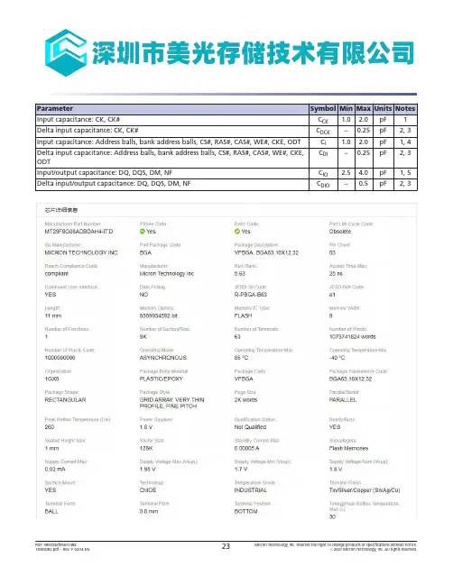
MTXO8LFTD中文资料
- 格式:pdf
- 大小:232.90 KB
- 文档页数:1


NAND Flash MemoryMT29F4G08ABADAH4, MT29F4G08ABADAWP, MT29F4G08ABBDAH4, MT29F4G08ABBDAHC, MT29F4G16ABADAH4, MT29F4G16ABADAWP, MT29F4G16ABBDAH4, MT29F4G16ABBDAHC, MT29F8G08ADADAH4,MT29F8G08ADBDAH4, MT29F8G16ADADAH4, MT29F8G16ADBDAH4, MT29F16G08AJADAWPFeatures•Open NAND Flash Interface (ONFI) 1.0-compliant1•Single-level cell (SLC) technology •Organization–Page size x8: 2112 bytes (2048 + 64 bytes)–Page size x16: 1056 words (1024 + 32 words)–Block size: 64 pages (128K + 4K bytes)–Plane size: 2 planes x 2048 blocks per plane–Device size: 4Gb: 4096 blocks; 8Gb: 8192 blocks 16Gb: 16,384 blocks•Asynchronous I/O performance–t RC/t WC: 20ns (3.3V), 25ns (1.8V)•Array performance–Read page: 25µs 3–Program page: 200µs (TYP: 1.8V, 3.3V)3–Erase block: 700µs (TYP)•Command set: ONFI NAND Flash Protocol •Advanced command set–Program page cache mode4–Read page cache mode 4–One-time programmable (OTP) mode–Two-plane commands 4–Interleaved die (LUN) operations–Read unique ID–Block lock (1.8V only)–Internal data move•Operation status byte provides software method for detecting–Operation completion–Pass/fail condition–Write-protect status•Ready/Busy# (R/B#) signal provides a hardware method of detecting operation completion•WP# signal: Write protect entire device •First block (block address 00h) is valid when ship-ped from factory with ECC. For minimum required ECC, see Error Management.•Block 0 requires 1-bit ECC if PROGRAM/ERASE cy-cles are less than 1000•RESET (FFh) required as first command after pow-er-on•Alternate method of device initialization (Nand_In-it) after power up (contact factory)•Internal data move operations supported within the plane from which data is read•Quality and reliability–Data retention: 10 years–Endurance: 100,000 PROGRAM/ERASE cycles •Operating voltage range–V CC: 2.7–3.6V–V CC: 1.7–1.95V•Operating temperature:–Commercial: 0°C to +70°C–Industrial (IT): –40ºC to +85ºC•Package–48-pin TSOP type 1, CPL2–63-ball VFBGANotes: 1.The ONFI 1.0 specification is available at2.CPL = Center parting line.3.See Program and Erase Characteristics fort R_ECC and t PROG_ECC specifications.4.These commands supported only with ECCdisabled.Figure 78: TWO-PLANE BLOCK ERASERE#CE#ALECLE I/Ox R/B#WE#Figure 79: TWO-PLANE/MULTIPLE-DIE READ STATUS CycleCE#CLE ALE RE#I/Ox4Gb, 8Gb, 16Gb: x8, x16 NAND Flash MemoryTwo-Plane OperationsInterleaved Die (Multi-LUN) OperationsIn devices that have more than one die (LUN) per target, it is possible to improve per-formance by interleaving operations between the die (LUNs). An interleaved die (multi-LUN) operation is one that is issued to an idle die (LUN) (RDY = 1) while another die (LUN) is busy (RDY = 0).Interleaved die (multi-LUN) operations are prohibited following RESET (FFh), identifi-cation (90h, ECh, EDh), and configuration (EEh, EFh) operations until ARDY =1 for all of the die (LUNs) on the target.During an interleaved die (multi-LUN) operation, there are two methods to determine operation completion. The R/B# signal indicates when all of the die (LUNs) have finish-ed their operations. R/B# remains LOW while any die (LUN) is busy. When R/B# goes HIGH, all of the die (LUNs) are idle and the operations are complete. Alternatively, the READ STATUS ENHANCED (78h) command can report the status of each die (LUN) in-dividually.If a die (LUN) is performing a cache operation, like PROGRAM PAGE CACHE (80h-15h),then the die (LUN) is able to accept the data for another cache operation when status register bit 6 is 1. All operations, including cache operations, are complete on a die when status register bit 5 is 1.During and following interleaved die (multi-LUN) operations, the READ STATUS (70h)command is prohibited. Instead, use the READ STATUS ENHANCED (78h) command to monitor status. This command selects which die (LUN) will report status. When two-plane commands are used with interleaved die (multi-LUN) operations, the two-plane commands must also meet the requirements in Two-Plane Operations.See Command Definitions for the list of commands that can be issued while other die (LUNs) are busy.During an interleaved die (multi-LUN) operation that involves a PROGRAM series (80h-10h, 80h-15h) operation and a READ operation, the PROGRAM series operation must be issued before the READ series operation. The data from the READ series opera-tion must be output to the host before the next PROGRAM series operation is issued.This is because the 80h command clears the cache register contents of all cache regis-ters on all planes.4Gb, 8Gb, 16Gb: x8, x16 NAND Flash MemoryInterleaved Die (Multi-LUN) OperationsError ManagementEach NAND Flash die (LUN) is specified to have a minimum number of valid blocks(NVB) of the total available blocks. This means the die (LUNs) could have blocks thatare invalid when shipped from the factory. An invalid block is one that contains at leastone page that has more bad bits than can be corrected by the minimum required ECC.Additional blocks can develop with use. However, the total number of available blocksper die (LUN) will not fall below NVB during the endurance life of the product.Although NAND Flash memory devices could contain bad blocks, they can be usedquite reliably in systems that provide bad block management and error-correction algo-rithms. This type of software environment ensures data integrity.Internal circuitry isolates each block from other blocks, so the presence of a bad blockdoes not affect the operation of the rest of the NAND Flash array.NAND Flash devices are shipped from the factory erased. The factory identifies invalidblocks before shipping by attempting to program the bad block mark into every loca-tion in the first page of each invalid block. It may not be possible to program every loca-tion with the bad block mark. However, the first spare area location in each bad block isguaranteed to contain the bad block mark. This method is compliant with ONFI FactoryDefect Mapping requirements. See the following table for the first spare area locationand the bad block mark.System software should check the first spare area location on the first page of eachblock prior to performing any PROGRAM or ERASE operations on the NAND Flash de-vice. A bad block table can then be created, enabling system software to map aroundthese areas. Factory testing is performed under worst-case conditions. Because invalidblocks could be marginal, it may not be possible to recover this information if the blockis erased.Over time, some memory locations may fail to program or erase properly. In order toensure that data is stored properly over the life of the NAND Flash device, the followingprecautions are required:•Always check status after a PROGRAM or ERASE operation•Under typical conditions, use the minimum required ECC (see table below)•Use bad block management and wear-leveling algorithmsThe first block (physical block address 00h) for each CE# is guaranteed to be validwith ECC when shipped from the factory.Table 21: Error Management DetailsTable 21: Error Management Details (Continued)。
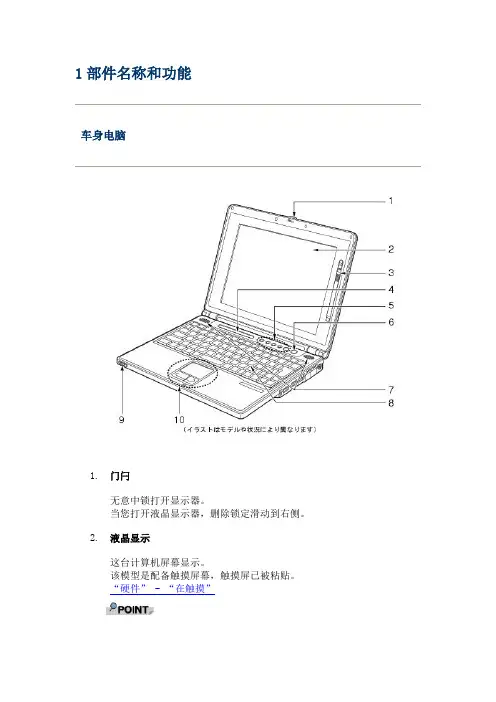
1部件名称和功能车身电脑1.门闩无意中锁打开显示器。
当您打开液晶显示器,删除锁定滑动到右侧。
2.液晶显示这台计算机屏幕显示。
该模型是配备触摸屏幕,触摸屏已被粘贴。
“硬件” - “在触摸”o液晶显示器的特点以下是LCD的特性。
这些都不是有瑕疵,请注意。
▪液晶显示技术,使我们非常准确,而不是光点在屏幕上的一些不,有可能点燃所有的点。
▪液晶显示器已经在这台电脑上使用,制造过程,产品的不同颜色可能会为每个。
底纹的颜色可能会出现一些其它温度。
▪后像可以继续使用相同的长远的眼光。
后像会消失,一段时间后。
为了防止这种行为,关闭显示器或使用省电功能,我们建议使用屏幕保护程序。
▪这种状况可能会出现轻微的显着点和不平衡的。
3.佩恩(触摸屏型号)存储一直与触摸笔。
“硬件” - “在触摸”4.LCD状态显示显示计算机的状态这一点。
名称“零件” - “关于LCD状态显示”5.安全按钮附加应用“安全按钮”或“一触式按键设置”可用于安装(→“软件”- “软件目录”)。
附加应用程序通过设置密码“安全按钮”,用户认证可以做到的。
陪同的应用,“一触式按键配置通过使用功能,您可以调用,只需按下一个按钮,您的电脑”。
“安全” - “按钮”安全6.电源按钮打开控制台或个人电脑,待机(挂起)/恢复(恢复)是使按钮。
o请按从04秒电源按钮。
按住〇四秒电源按钮,计算机将关闭电源。
7.扬声器PC音频书籍印刷。
“函数” - “音量设置”o音量,请调整范围从扬声器Hizumanai声音设置和声音。
造成损坏扬声器。
8.键盘键入字符可以号令到PC。
“硬件” - “在键盘上”9.无线交换机(无线局域网模式只)无线局域网通信ON和OFF。
医院和飞机,在那里,请在设备限制使用其他电子开关为OFF。
o对于无线局域网,“Kasutamumeidoopushon”手册中请。
10. 平特操纵鼠标指针。
“硬件” - “为指针。
”体表电脑1.集成无线局域网天线(无线局域网模式只)内置的无线局域网天线。
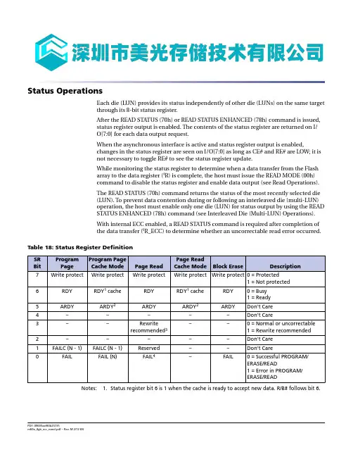
Status OperationsEach die (LUN) provides its status independently of other die (LUNs) on the same targetthrough its 8-bit status register.After the READ STATUS (70h) or READ STATUS ENHANCED (78h) command is issued,status register output is enabled. The contents of the status register are returned on I/O[7:0] for each data output request.When the asynchronous interface is active and status register output is enabled,changes in the status register are seen on I/O[7:0] as long as CE# and RE# are LOW; it isnot necessary to toggle RE# to see the status register update.While monitoring the status register to determine when a data transfer from the Flasharray to the data register (t R) is complete, the host must issue the READ MODE (00h)command to disable the status register and enable data output (see Read Operations).The READ STATUS (70h) command returns the status of the most recently selected die(LUN). To prevent data contention during or following an interleaved die (multi-LUN)operation, the host must enable only one die (LUN) for status output by using the READSTATUS ENHANCED (78h) command (see Interleaved Die (Multi-LUN) Operations).With internal ECC enabled, a READ STATUS command is required after completion ofthe data transfer (t R_ECC) to determine whether an uncorrectable read error occurred. Table 18: Status Register DefinitionNotes: 1.Status register bit 6 is 1 when the cache is ready to accept new data. R/B# follows bit 6.Read OperationsThe READ PAGE (00h-30h) command, when issued by itself, reads one page from theNAND Flash array to its cache register and enables data output for that cache register.During data output the following commands can be used to read and modify the data inthe cache registers: RANDOM DATA READ (05h-E0h) and RANDOM DATA INPUT (85h).Read Cache OperationsTo increase data throughput, the READ PAGE CACHE series (31h, 00h-31h) commandscan be used to output data from the cache register while concurrently copying a pagefrom the NAND Flash array to the data register.To begin a read page cache sequence, begin by reading a page from the NAND Flash ar-ray to its corresponding cache register using the READ PAGE (00h-30h) command.R/B# goes LOW during t R and the selected die (LUN) is busy (RDY = 0, ARDY = 0). Aftert R (R/B# is HIGH and RDY = 1, ARDY = 1), issue either of these commands:•READ PAGE CACHE SEQUENTIAL (31h) – copies the next sequential page from theNAND Flash array to the data register•READ PAGE CACHE RANDOM (00h-31h) – copies the page specified in this commandfrom the NAND Flash array to its corresponding data registerAfter the READ PAGE CACHE series (31h, 00h-31h) command has been issued, R/B#goes LOW on the target, and RDY = 0 and ARDY = 0 on the die (LUN) for t RCBSY whilethe next page begins copying data from the array to the data register. After t RCBSY,R/B# goes HIGH and the die’s (LUN’s) status register bits indicate the device is busywith a cache operation (RDY = 1, ARDY = 0). The cache register becomes available andthe page requested in the READ PAGE CACHE operation is transferred to the data regis-ter. At this point, data can be output from the cache register, beginning at column ad-dress 0. The RANDOM DATA READ (05h-E0h) command can be used to change the col-umn address of the data output by the die (LUN).After outputting the desired number of bytes from the cache register, either an addi-tional READ PAGE CACHE series (31h, 00h-31h) operation can be started or the READPAGE CACHE LAST (3Fh) command can be issued.If the READ PAGE CACHE LAST (3Fh) command is issued, R/B# goes LOW on the target,and RDY = 0 and ARDY = 0 on the die (LUN) for t RCBSY while the data register is copiedinto the cache register. After t RCBSY, R/B# goes HIGH and RDY = 1 andARDY = 1, indicating that the cache register is available and that the die (LUN) is ready.Data can then be output from the cache register, beginning at column address 0. TheRANDOM DATA READ (05h-E0h) command can be used to change the column addressof the data being output.For READ PAGE CACHE series (31h, 00h-31h, 3Fh), during the die (LUN) busy time,t RCBSY, when RDY = 0 and ARDY = 0, the only valid commands are status operations(70h, 78h) and RESET (FFh). When RDY = 1 and ARDY = 0, the only valid commandsduring READ PAGE CACHE series (31h, 00h-31h) operations are status operations (70h,78h), READ MODE (00h), READ PAGE CACHE series (31h, 00h-31h), RANDOM DATAREAD (05h-E0h), and RESET (FFh).Two-Plane Read OperationsTwo-plane read page operations improve data throughput by copying data from more than one plane simultaneously to the specified cache registers. This is done by pre-pending one or more READ PAGE TWO-PLANE (00h-00h-30h) commands in front of the READ PAGE (00h-30h) command.When the die (LUN) is ready, the RANDOM DATA READ TWO-PLANE (06h-E0h) com-mand determines which plane outputs data. During data output, the following com-mands can be used to read and modify the data in the cache registers: RANDOM DATA READ (05h-E0h) and RANDOM DATA INPUT (85h).Two-Plane Read Cache OperationsTwo-plane read cache operations can be used to output data from more than one cache register while concurrently copying one or more pages from the NAND Flash array to the data register. This is done by prepending READ PAGE TWO-PLANE (00h-00h-30h) commands in front of the PAGE READ CACHE RANDOM (00h-31h) command.To begin a two-plane read page cache sequence, begin by issuing a READ PAGE TWO-PLANE operation using the READ PAGE TWO-PLANE (00h-00h-30h) and READ PAGE (00h-30h) commands. R/B# goes LOW during t R and the selected die (LUN) is busy (RDY = 0, ARDY = 0). After t R (R/B# is HIGH and RDY = 1, ARDY = 1), issue either of these commands:•READ PAGE CACHE SEQUENTIAL (31h) – copies the next sequential pages from the previously addressed planes from the NAND Flash array to the data registers.•READ PAGE TWO-PLANE (00h-00h-30h) [in some cases, followed by READ PAGE CACHE RANDOM (00h-31h)] – copies the pages specified from the NAND Flash array to the corresponding data registers.After the READ PAGE CACHE series (31h, 00h-31h) command has been issued, R/B# goes LOW on the target, and RDY = 0 and ARDY = 0 on the die (LUN) for t RCBSY while the next pages begin copying data from the array to the data registers. After t RCBSY,R/B# goes HIGH and the LUN’s status register bits indicate the device is busy with a cache operation (RDY = 1, ARDY = 0). The cache registers become available and the pa-ges requested in the READ PAGE CACHE operation are transferred to the data registers. Issue the RANDOM DATA READ TWO-PLANE (06h-E0h) command to determine which cache register will output data. After data is output, the RANDOM DATA READ TWO-PLANE (06h-E0h) command can be used to output data from other cache registers. Af-ter a cache register has been selected, the RANDOM DATA READ (05h-E0h) command can be used to change the column address of the data output.After outputting data from the cache registers, either an additional TWO-PLANE READ CACHE series (31h, 00h-31h) operation can be started or the READ PAGE CACHE LAST (3Fh) command can be issued.If the READ PAGE CACHE LAST (3Fh) command is issued, R/B# goes LOW on the target, and RDY = 0 and ARDY = 0 on the die (LUN) for t RCBSY while the data registers are cop-ied into the cache registers. After t RCBSY, R/B# goes HIGH and RDY = 1 and ARDY = 1, indicating that the cache registers are available and that the die (LUN) is ready. Issue the RANDOM DATA READ TWO-PLANE (06h-E0h) command to determine which cache register will output data. After data is output, the RANDOM DATA READ TWO-PLANE (06h-E0h) command can be used to output data from other cache registers. After a cache register has been selected, the RANDOM DATA READ (05h-E0h) command can be used to change the column address of the data output.output begins at the column address last specified in the READ PAGE (00h-30h) com-mand. The RANDOM DATA READ TWO-PLANE (06h-E0h) command is used to enabledata output in the other cache registers.Figure 38: READ PAGE (00h-30h) OperationCycle typeI/O[7:0]RDYFigure 39: READ PAGE (00h-30h) Operation with Internal ECC EnabledRDYSR bit 1 = 0 READ errorREAD PAGE CACHE SEQUENTIAL (31h)The READ PAGE CACHE SEQUENTIAL (31h) command reads the next sequential pagewithin a block into the data register while the previous page is output from the cacheregister. This command is accepted by the die (LUN) when it is ready(RDY = 1, ARDY = 1). It is also accepted by the die (LUN) during READ PAGE CACHE(31h, 00h-31h) operations (RDY = 1 and ARDY = 0).To issue this command, write 31h to the command register. After this command is is-sued, R/B# goes LOW and the die (LUN) is busy (RDY = 0, ARDY = 0) for t RCBSY. Aftert RCBSY, R/B# goes HIGH and the die (LUN) is busy with a cache operation(RDY = 1, ARDY = 0), indicating that the cache register is available and that the specifiedpage is copying from the NAND Flash array to the data register. At this point, data canbe output from the cache register beginning at column address 0. The RANDOM DATAREAD (05h-E0h) command can be used to change the column address of the data beingoutput from the cache register.The READ PAGE CACHE SEQUENTIAL (31h) command can be used to cross blockboundaries. If the READ PAGE CACHE SEQUENTIAL (31h) command is issued after thelast page of a block is read into the data register, the next page read will be the next logi-cal block in which the 31h command was issued. Do not issue the READ PAGE CACHESEQUENTIAL (31h) to cross die (LUN) boundaries. Instead, issue the READ PAGECACHE LAST (3Fh) command.。