微电子封装课程导论
- 格式:pdf
- 大小:12.14 MB
- 文档页数:74

第3章微电子的封装技术微电子封装技术是指对集成电路芯片进行外包装和封封装的工艺技术。
封装技术的发展对于提高微电子产品的性能、减小体积、提高可靠性和降低成本具有重要意义。
封装技术的目标是实现对芯片的保护和有效连接,同时满足对尺寸、功耗、散热、信号传输等方面的要求。
封装技术的发展经历了多个阶段。
早期的微电子产品采用插入式封装,芯片通过引脚插入芯片座来连接电路板,这种封装方式容易受到环境的影响,连接不可靠,也无法满足小型化和高集成度的需求。
后来,绝缘层封装技术得到了广泛应用,通过在芯片上覆盖绝缘层,然后连接金属线路,再通过焊接或压力连接的方式实现芯片与电路板之间的连接。
这种封装方式提高了连接的可靠性,但由于绝缘层的存在,芯片的散热能力受到限制。
随着技术的进步,微电子封装技术也得到了快速发展。
现代微电子产品普遍采用半导体封装技术,具有体积小、功耗低、可靠性强和成本低等优点。
常见的半导体封装技术有裸片封装、焊接封装和微球栅阵列封装等。
裸片封装是将芯片裸露在外界环境中,并通过焊接或压力连接的方式与电路板相连。
这种封装方式具有体积小、重量轻和散热能力强的优点,但对芯片的保护较差,容易受到外界的机械和热力作用。
焊接封装是将芯片与封装底座通过焊接的方式连接起来。
常见的焊接技术有电离子焊接、激光焊接和超声波焊接等。
电离子焊接是利用高能电子束将封装底座和芯片焊接在一起,具有连接可靠、焊接速度快的优点。
激光焊接利用激光束对焊接点进行加热,实现焊接。
超声波焊接则是利用超声波的振动将焊接点熔化,并实现连接。
焊接封装具有连接可靠、工艺简单和尺寸小的优点,但要求焊接点的精度和尺寸控制较高。
微球栅阵列封装是一种先进的封装技术,其特点是将芯片中的引脚通过微小球连接到封装底座上。
这种封装方式不仅提高了信号传输的速度和可靠性,还可以实现更高的封装密度和更小的封装尺寸。
微球栅阵列封装需要使用高精度的装备和工艺,但具有很大的发展潜力。
除了封装技术的发展,微电子封装材料的研究也十分重要。
![微电子封装技术讲义06.07[1]](https://uimg.taocdn.com/8423da2c5acfa1c7aa00ccc4.webp)
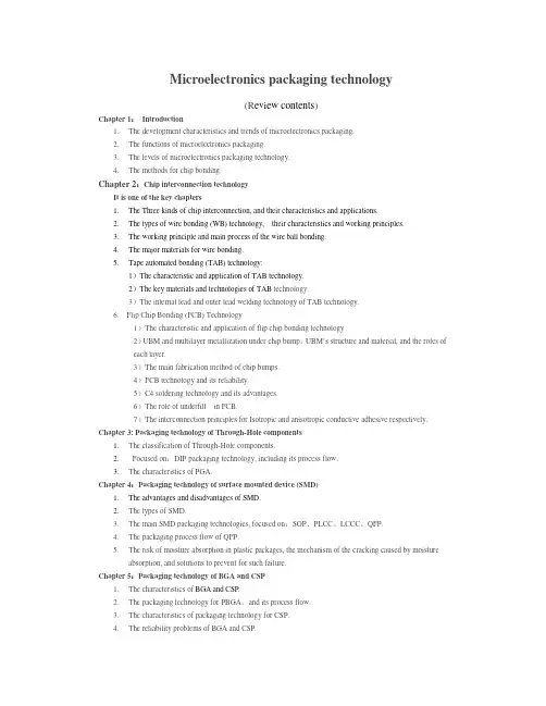
Microelectronics packaging technology(R eview contents)Chapter 1:Introduction1.The development characteristics and trends of microelectronics packaging.2.The functions of microelectronics packaging.3.The levels of microelectronics packaging technology.4.The methods for chip bonding.Chapter 2:Chip interconnection technologyIt is one of the key chapters1.The Three kinds of chip interconnection, and their characteristics and applications.2.The types of wire bonding (WB) technology, their characteristics and working principles.3.The working principle and main process of the wire ball bonding.4.The major materials for wire bonding.5.Tape automated bonding (TAB) technology:1)The characteristic and application of TAB technology.2)The key materials and technologies of TAB technology.3)The internal lead and outer lead welding technology of TAB technology.6. Flip Chip Bonding (FCB) Technology1)The characteristic and application of flip chip bonding technology2)UBM and multilayer metallization under chip bump;UBM’s structure and material, and the roles ofeach layer.3)The main fabrication method of chip bumps.4)FCB technology and its reliability.5)C4 soldering technology and its advantages.6)The role of underfill in FCB.7)The interconnection principles for Isotropic and anisotropic conductive adhesive respectively. Chapter 3: Packaging technology of Through-Hole components1.The classification of Through-Hole components.2.Focused on:DIP packaging technology, including its process flow.3.The characteristics of PGA.Chapter 4:Packaging technology of surface mounted device (SMD)1.The advantages and disadvantages of SMD.2.The types of SMD.3.The main SMD packaging technologies, focused on:SOP、PLCC、LCCC、QFP.4.The packaging process flow of QFP.5.The risk of moisture absorption in plastic packages, the mechanism of the cracking caused by moistureabsorption, and solutions to prevent for such failure.Chapter 5:Packaging technology of BGA and CSP1.The characteristics of BGA and CSP.2.The packaging technology for PBGA,and its process flow.3.The characteristics of packaging technology for CSP.4.The reliability problems of BGA and CSP.Chapter 6:Multi-Chip Module(MCM)1.The classification and characteristics of MCM2. The assembly technology of MCM.Chapter 7:Electronic packaging materials and substrate technology1. The classification of the materials for electronic packaging, the main requirements for packagingmaterials.2. The types of metals in electronic packaging, and their main applications.3. The main requirements for polymer materials in electronic packaging.4.Classification of main substrate materials, and the major requirements for substrate materials.Chapter 8:Microelectronics packaging reliability1.The basic concepts of electronic packaging reliability.2.The basic concepts for failure mode and failure mechanism in electronic packaging.3.Main failure (defect) modes (types) of electronic packaging.4.The purpose and procedure of failure analysis (FA) ;Common FA techniques (such as cross section, dyeand pry, SEM, CSAM ...).5 The purpose and key factors (such as stress level, stress type …) to design accelerated reliability test. Chapter 9:Advanced packaging technologies1.The concept of wafer level packaging (WLP) technology.2.The key processes of WL-CSP.3.The concept and types of the 3D packaging technologies.Specified Subject 1:LED packaging technology1. Describe briefly the four ways to achieve LED white light, and how they are packaged?2. Describe briefly the difference and similar aspects (similarity) between LED packaging andmicroelectronics packaging.3. And also describe briefly the development trend for LED package technology and the whole LED industryrespectively.Specified Subject 2:MEMS packaging technology1.The differences between micro-electro-mechanical system (MEMS) packaging technology and theconventional microelectronics packaging technologies.2.The function requirements of MEMS packaging.Extra requirement:The common used terms (Abbreviation) for electronic packaging.。
《电子封装技术专业学科(专业)概论》课程教学大纲一、课程名称(中英文)中文名称:学科(专业)概论英文名称:An Introduction to Discipline (Specialty)二、课程编码及性质课程编码:0400022课程性质:必修课三、学时与学分总学时:16学分:1四、先修课程军训、入学教育、实验室参观五、授课对象本课程面向刚入校的“电子封装技术专业”学生,也可以供“电子制造科学与工程专业”和“微电子工程专业”入学新生选修。
六、课程教学目的本课程是本专业入学新生快速了解专业领域的历史、现状、发展,培养学生专业兴趣的导入与介绍课程。
主要包括:1.系统介绍从电子管、半导体、集成电路再到信息电子产品的制造发展历程,理解信(信息电子产品)和衣、食、住、行相提并论,成为人们现代人们生活的必须(需),从而深入掌握信息电子产品制造的内涵、外延;2.介绍本专业的教学规划、教学体系、四年的课程安排,各课程的特色与相互关联,培养新生四年大学学习与生活的规划能力;3.重点介绍集成电路制造、电子封装技术、电子组装技术、半导体照明、太阳能光伏、电子显示技术等的基本知识、应用领域、发展方向,理解人类未来电子产品制造的蓝图;4.培养学生从事电子制造领域的素质和能力。
表1 课程目标对毕业要求的支撑关系七、教学重点与难点:教学重点:1)向学生介绍本专业的基本状况与发展前景,激发学生对本专业的兴趣,立志投身中国的电子制造业;2)介绍本专业的教学规划、教学体系、四年的课程安排,介绍各课程的特色与相互关联;3)重点介绍集成电路制造、电子封装技术、电子组装技术、半导体照明、太阳能光伏、电子显示技术等的基本知识、应用领域、发展方向。
教学难点:学科(专业)概论是电子封装技术专业的必修课程,具有入门、宏观、概要等特征,对学生的四年专业学习起着引领、指导、启发等作用,是进入大学学习的最重要认识课程。
由本专业的资深教授讲授,间或聘请专业领域的著名人士以专题讲座形式进行。
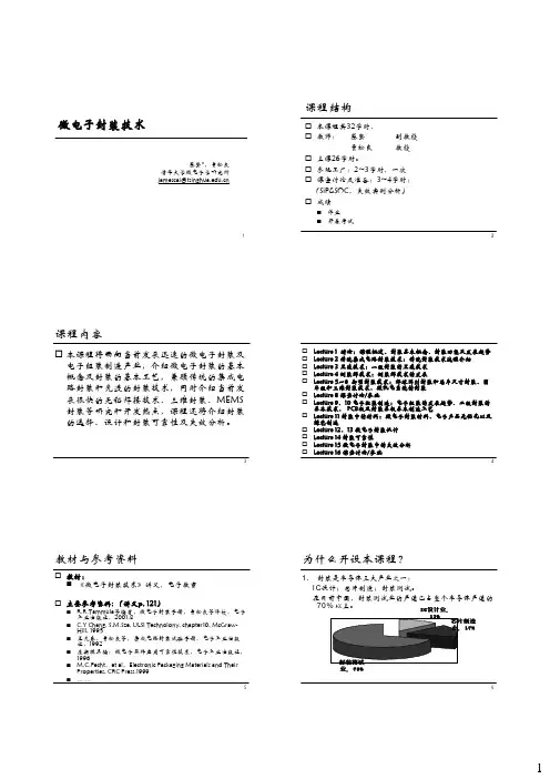
1微电子封装技术蔡坚*,贾松良清华大学微电子学研究所jamescai@2课程结构本课程共32学时, 教师:蔡坚副教授贾松良教授上课26学时。
参观工厂:2‾3学时,一次 课堂讨论及准备:3‾4学时:(SiP&SOC,失效实例分析) 成绩作业 开卷考试3课程内容本课程将面向当前发展迅速的微电子封装及电子组装制造产业,介绍微电子封装的基本概念及封装的基本工艺,兼顾传统的集成电路封装和先进的封装技术,同时介绍当前发展很快的无铅焊接技术、三维封装、MEMS 封装等研究和开发热点,课程还将介绍封装的选择、设计和封装可靠性及失效分析。
4Lecture 1 绪论:课程概述、封装基本概念、封装功能及发展趋势 Lecture 2 传统集成电路封装技术:传统封装技术流程介绍 Lecture 3 互连技术:一级封装的互连技术 Lecture 4 倒装焊技术:倒装焊技术的发展Lecture 5~6 新型封装技术:焊球阵列封装和芯片尺寸封装、圆片级和三维封装技术、微机电系统的封装 Lecture 8 课堂讨论/参观Lecture 9、10 电子组装制造:电子组装的发展趋势、二级封装的基本技术、PCB板及封装基板基本制造工艺Lecture 11 封装中的材料:微电子封装材料、电子产品无铅化以及绿色制造Lecture 12、13 微电子封装设计 Lecture 14 封装可靠性Lecture 15 微电子封装中的失效分析Lecture 16 课堂讨论/参观5教材与参考资料教材:《微电子封装技术》讲义、电子教案 主要参考资料: (讲义p. 121)R.R.Tammula等编著,微电子封装手册,贾松良等译校,电子工业出版社,2001.8C.Y Chang, S.M.Sze, ULSI Technolony, chapter10, McGraw-Hill, 1995王先春、贾松良等,集成电路封装试验手册,电子工业出版社,1992庄奕琪主编:微电子器件应用可靠性技术,电子工业出版社,1996M.C.Pecht,et al,Electronic Packaging Materials and TheirProperties, CRC Press.1999 ……6为什么开设本课程?1.封装是半导体三大产业之一:IC 设计;芯片制造;封装测试。