教学EN_cadence+spectre+使用手册
- 格式:pdf
- 大小:801.74 KB
- 文档页数:21
cadence教程Cadence 是一款流行的电路设计和仿真工具。
它广泛应用于电子工程领域,可以帮助工程师进行电路设计、布局、仿真和验证。
以下是一个简单的 Cadence 教程,帮助你快速入门使用该软件。
第一步: 下载和安装 Cadence首先,你需要从 Cadence 官方网站下载适用于你操作系统的Cadence 软件安装包。
在下载完成后,双击安装包文件并按照安装向导的指示进行安装。
第二步: 创建新项目打开 Cadence 软件后,你将看到一个初始界面。
点击“File”菜单,然后选择“New”来创建一个新的项目。
第三步: 添加电路元件在新项目中,你可以开始添加电路元件。
点击菜单栏上的“Library”按钮,然后选择“Add Library”来添加一个元件库。
接下来,使用菜单栏上的“Place”按钮来添加所需的电路元件。
第四步: 连接电路元件一旦添加了电路元件,你需要使用连线工具来连接它们。
点击菜单栏上的“Place Wire”按钮,然后将鼠标指针移到一个元件的引脚上。
点击引脚,然后按照电路的设计布局开始连接其他元件。
第五步: 设置仿真参数在完成电路布局后,你需要设置仿真参数。
点击菜单栏上的“Simulate”按钮,然后选择“Configure”来设置仿真器类型、仿真时间等参数。
第六步: 运行仿真设置完成后,你可以点击菜单栏上的“Simulate”按钮,然后选择“Run”来运行仿真。
仿真过程会模拟电路的运行情况,并生成相应的结果。
总结通过这个简单的 Cadence 教程,你了解了如何下载安装Cadence 软件、创建新项目、添加电路元件、连接元件、设置仿真参数和运行仿真。
掌握了这些基本操作后,你可以进一步学习和探索 Cadence 的更多功能和高级技巧。
祝你在使用Cadence 中取得成功!。
cadence指导详细版⼀、cadence软件及安装指导1、安装虚拟机,安装过程中需要添加中的Serial(注意:⼀旦安装成功不要轻易卸载,否则重装很费劲)2、在windows下解压cadence⽂件夹下压缩包3、双击桌⾯虚拟机图标,打开虚拟机,点击界⾯左上⾓FILE》》open》》在弹出的对话框内找到刚刚解压的cadence⽂件夹下的⽂件,点击“打开”4、点击power on this virtual machine ,输⼊⽤户名 zyx,密码 1234565、我们进⼊到了linux系统。
⼆、 NCSU 库的加载及cadecne的环境配置1、直接将⽂件夹ncsu-cdk-1.5.1拷贝到linux系统桌⾯。
(若直接复制不成功,可通过U盘将其导⼊。
)2、打开桌⾯zyx’Home⽬录(即⽂件夹),在⾥⾯新建⽬录VLSI,将桌⾯ncsu-cdk-1.5.1剪切⾄VLSI⽬录下。
3、在桌⾯空⽩处单击⿏标右键,点击open Teminal4、在终端内输⼊以下命令。
1、 su root -------进⼊到超级⽤户2、 sunface8211200 (不可见,直接输⼊即可)3、 chmod a+w ------修改权限后,可以对其进⾏编写4、 vi --------进⼊到vi 编辑器,单击键盘“ i ”进⼊到插⼊模式,在第⼀⾏我们添加⼀⾏语句。
INCLUDE /home/zyx/VLSI/ncsu-cdk-1.5.1/cdssetup/输⼊完之后,单击键盘“esc”键退出插⼊模式,再点击键盘“:wq ”退出vi编辑器5、cd VLSI/ncsu-cdk-1.5.1/cdssetup ---------进⼊到cdssetup⽬录6、 vi --------做如下图修改后,点击esc键并输⼊“:wq ”退出7、csh -------进⼊到c shell命令8、vi /home/zyx/.cshrc ------进⼊到⽤户⽬录下的 .cshrc的编写,并添加如下语句setenv CDK_DIR /home/zyx/VLSI/ncsu-cdk-1.5.1 ,添加后“:wq ”保存退出9、cp cdsinit /home/zyx/.cdsinit10、cp /home/zyx/11、⾄此,⼯艺库安装完毕,cadence环境配置也已经结束。
cadence使用方法Cadence 是一种流行的电子设计自动化(EDA)工具,用于VLSI(Very Large Scale Integration)设计和仿真。
它由美国卡内基梅隆大学的Circuit Design Group开发,是IC设计工程师广泛使用的一种工具。
Cadence 提供了一整套的工具,包括电路设计、物理布局、封装设计以及信号完整性仿真等。
1.工程设置:在开始之前,你需要设置你的工程。
这包括指定设计库和工作目录。
你可以在Cadence的命令行界面输入"set"命令,设置Cadence工程的相关参数。
2.电路设计:在Cadence中,你可以使用Virtuoso Schematic Editor或者Silicon Ensemble Schematic Editor进行电路设计。
你可以从菜单中选择相应的元件,然后将它们拖放到画布上,并连接它们。
你还可以设置元件的参数和属性。
3.电路仿真:完成电路设计后,你可以使用Spectre或者HSPICE等仿真工具来验证你的设计。
你需要定义相应的仿真参数,如仿真器类型、仿真时间等。
Cadence还提供了仿真结果的分析和波形显示,以便你评估电路的性能和稳定性。
4.物理布局:5.物理验证:完成物理布局后,你需要进行物理验证,以确保设计的可制造性和可靠性。
Cadence提供了Innovus和Tempus等工具,用于进行电压引脚冲突检查、信号完整性分析和时序分析等。
这些工具可以帮助你发现潜在的物理问题,并提供相应的解决方案。
6.封装设计:在完成物理验证后,你需要设计封装。
Cadence提供了封装设计工具,如Allegro Package Designer。
你可以定义芯片的引脚布局和间距规则,并生成封装文件。
7.电路板设计:当你完成芯片设计后,你可能需要进行电路板设计。
Cadence提供了Allegro PCB Designer等工具,用于进行电路板布局和连线。

Cadence IC Design ManualFor EE5518ZHENG Huan QunLin Long YangRevised onMay 2017Department of Electrical & Computer EngineeringNational University of SingaporeContents1 INTRODUCTION (4)1.1 Overview of Design Flow (4)1.2 Getting Started with Cadence (6)1.3 Using Online Help (8)1.4 Exit Cadence (8)2 SCHEMATIC ENTRY (9)2.1 Creating a New Design Library (9)2.2 Creating a Schematic Cellview (10)2.3 Adding Components to Schematic (11)2.4 Adding Pins to Schematic (12)2.5 Adding Wires to Schematic (13)2.6 Saving Your Design (14)3 SYMBOL AND TEST CIRCUIT CREATION (15)3.1 Creating Symbol (15)3.2 Editing Symbol (16)3.3 Building Test Bench (18)4 SIMULATING YOUR CIRCUIT (21)4.1 Start the Simulation Environment (21)4.2 Selecting Project Directory (21)4.3 Setup Model Library (22)4.4 Choosing the Desired Analysis (22)4.5 Setup Variables (23)4.6 Saving Simulation Data (24)4.7 Saving Output for Plotting (24)4.8 Viewing the Netlists (25)4.9 Running the Simulation (25)5 PHYSICAL LAYOUT (28)5.1 Layout vs Symbol of CMOS Devices (28)5.2 Starting Layout Editor (29)5.3 Vias (31)5.4 Changing the Grid (33)5.5 Inserting and Editing Instances (34)5.6 Drawing Shapes / Paths (35)5.7 Creating Pins (36)6 DESIGN VERIFICATION: DRC AND LVS (38)6.1 Performing DRC (38)6.2 Performing LVS (40)6.3 Performing PEX (41)7 POST‐LAYOUT SIMULATION (45)7.1 Simulation the Extracted Cell View (45)8 CONCLUSION (46)1INTRODUCTIONThis manual describes how to use Cadence IC design tools. It covers the whole design cycle, from the front-end to the back-end, i.e., from the pre-layout design to the post-layout design.The manual aims to provide a guide for fresh users. Following the manual, users can start doing analog IC design even though the users don’t have any knowledge of the tools.An inverter is used to illustrate the whole cycle of analog IC design, and Cadence Generic 45nm (cg45nm) kit is the technology library used for implementing the inverter. The method stated in the manual can be applied to other type of analog circuit design.1.1Overview of Design FlowFigure 1 shows a typical analog IC design flow.The design flow starts from schematic entry with the Cadence schematic capture tool –Schematic Editor. Devices or cells from the cg45nm or other libraries are used to build your circuit. Your design is hierarchical; therefore higher level schematics also incorporate cells which you have already developed. The schematics which you enter at this stage therefore typically consist of a number of base library cells and also lower level cells designed yourself.These are described in Sections 2 and 3 of the manual.When you have finished designing a particular circuit, you need to simulate it to ensure that it works as expected. It would be unlikely that your circuit works as expected at the first time so you have to repeat the cycle to improve the circuit, as shown in Figure 1, until the circuit works satisfactorily. This must be done for each sub-circuit of your design and then for the top level design. How to simulate and view the performance of simulation results are presented in Sections 4 of the manual.When the performance of the circuit is satisfactory, it is ready to start the physical design or layout of the circuit. The layout starts with the cell or device placement. Once the cells have been placed, routing can be carried out. Routing connects the cells/device of the design.After finishing placement and routing, the layout has to go through the Design Rule Check (DRC) with rule decks provided by PDK provider, to ensure that there is no design rule violation in the layout. The layout has to be rectified accordingly to the rules’ requirement till it passes DRC.Upon a successful DRC, it is Layout-versus-Schematic (LVS) check, to assure that all connections in the layout are correct. The layout has to be amended accordingly to the schematic If LVS doesn’t pass. DRC has to be done whenever layout is changed. The process is repeated until the LVS passes.Figure 1. Analog IC Design FlowThe next step is parasitic extraction (PEX) to get the extracted view of the circuit, which is used for post–layout simulation. The extracted view includes the parasitic effects in both the instances/devices and the required wiring interconnects of the circuit.Following DRC, LVS and PEX, it is post-layout simulation. The post-layout simulation is essential to make sure that the circuit with the extra parasitic parameters functions well and still meet the design specifications. If the performance of the post-layout simulation is not acceptable, back to the stage of schematic entry to check the circuit. Basically, re-design the circuit is necessary. Repeat the whole flow until the results of the post-layout simulation meet the design specifications.If everything is satisfactory, the next stage is GDSII Generation. It generates a file which depicts the low level geometry of layout. GDSII format is industry standard format suitable fora semiconductor company to fabricate and manufacture the chip of layout. This is briefed inthe last section of the manual.1.2Getting Started with CadenceUpon logging into your account, you will be brought to the Linux Desktop Environment.Right click on the desktop and click Open Terminal to open a “window” on the desktop. This window is the Linux command line prompt at which you can run Linux commands. After running a Linux command, this window also shows the output of the command.The following steps show how to start Cadence with cg45nm kit.A.Create a working directory - project (it can be any name as you like) with thecommand:mkdir projectwhere mkdir is Linux command and the project is the directory name;B.Enter the working directory with the command:cd projectwhere the cd is the Linux command;C.Type the followings commands to do the environment setup for using Cadence Generic45nm PDK.cp /app11/cg45nm/USERS/cds.lib .cp /app11/cg45nm/USERS/assura_tech.lib .cp /app11/cg45nm/USERS/pvtech.lib .D.Start cadence in the working directory – project with the following command:virtuoso &where virtuoso is the command to start Cadence IC design tool.Now, Cadence tools are successfully started. Keeps only the Command Input Window (CIW) which is shown in Figure 2.Figure 2. CIW WindowDo not close this CIW and try to keep it in view whenever you are using Cadence. Error messages and output from some of the tools are always sent to the CIW. If something doesn't appear to be working, always check the CIW for error messages. In addition, the CIW allows the user great control over Cadence by interpreting skill commands which are typed into it.E.In the CIW, select Tools Library Manager. The Library Manager pop up as inFigure 3. The Library Manager is where you create, add, copy, delete and organizeyour libraries and cell views.Figure 3. Library Manager WindowYou can see that the library gpdk045 appears in the Library column of the librarymanager.Now, you have started Cadence tool and loaded the cg45nm kit successfully. There are some documents in /app11/cg45nm/ gpdk045_v4_0/docs, and you can always refer to these documents for the information such as devices, device models, DRC rules and others related to cg45nm kit.Next time, you need only to repeat the steps B and D, for launching Cadence virtuoso and doing your project.1.3Using Online HelpCadence provides a comprehensive online manuals for all Cadence tools. You can launch the online help by typing the following command at the Linux prompt.cdnshelpThis invokes the online software manuals. Alternately, there is a help menu on each Cadence window. Manual which is related to that window related will pop-up once clicking on the help button.1.4Exit CadenceTo exit Cadence, just click on the cross sign X or File Exit in CIW. It is necessary to exit Cadence when it is not in use. Your library file would be locked or cannot edited next time if Cadence was not exited properly.2SCHEMATIC ENTRYNow that Cadence is running, you are almost ready to start entering schematics. However, you must first create a library which will be used to store all the parts of your design. Then, schematic can be created in the library.2.1Creating a New Design LibraryA.In the Library Manager window, select File→New→Library. New Library formpops up as shown in Figure 4.B.In the New Library form referring to Figure 4, key in your design library name(example: test) in the field of Name, and then click Ok.C.Click Ok in the pop-up window - the Technology File for New Library, referring toFigure 5.D.Choose gpdk045 in the Attach Library to Technology Library form, referring toFigure 6, and then click Ok.Figure 4. New Library FormFigure 5. Technology File for New Library FormFigure 6. Attach Library to Technology File FormA new library, named test, should appear in your Library Manager window.2.2 Creating a Schematic CellviewA.In Library Manager, select the Library where you would like to create a schematic. Then,select File→New→Cell View.B.Set up the New File form as Figure 7Figure 7. Create CellViewC.Click OK when done. A blank schematic window for the "inv" (your cell name)schematic appears.Explore the functions available by putting your mouse over the toolbar and fixed menu icons.In addition, note that some of the menu selections have alphabets listed to the right of them. These are bind-key or shortcut-key definitions which are very useful in the long run.Test them out during the schematic drawing in subsequent steps.2.3Adding Components to SchematicFigure 8 shows the schematic which you are going to patch, and the property of each component is listed in Table 1.Figure 8. Inverter CircuitTabel 1. Component Properties of Figure 8: Inverter CircuitComponents Library Name Cell Name PropertiesPMOS gpdk045 pmos1v l:45nm w:120nm (default size)NMOS gpdk045 nmos1v l:45nm w:120nm (default size)Here is the example on how to add component instances by placing cell views from libraries. Type “i” bind-key or select Create Instance in the schematic window or click on the menu bar to display Add Instance form. Then in the Add Instance window, select gpdk045as Library, choose the NMOS transistor by selecting nmos1v in Cell and also choose symbol as View, as shown in Figure 9.Figure 9. Add Instance FormSimilarly, add the pmos1v into the schematic. As an example, here we just keep all theparameters as default.If you place a component with the wrong parameter values, select the component and type “q” bindkey or use the Edit→Properties→Objects command to change the parameters. Use the Edit→Move command or type “m” if you place components in the wrong location.2.4Adding Pins to SchematicYou must place I/O pins in your schematic to identify the inputs and the outputs. A pin can be an input, output or an input-output (bi-directional) pin.Type “p” or select Add →Pin from inv Schematic Window or click the Pin fixed menuicon in the schematic window. The Add Pin form appears as Figure 10.Figure 10. Add Pin FormClick Hide and move you cursor to the Schematic Window. Place pins at the correct places and click right mouse key to rotate the pin if necessary.Add pins according to Table 2, paying attention to the direction.Table 2. Pin Names and Direction of invPin Names DirectionVin InputVout OutputVDD, GND Input-OutputCaution: Do not use the add component form to place schematic pins.2.5 Adding Wires to SchematicAdd wires to connect the components and pins in the design.A.Type “w” or select Add →Wire (narrow) in Schematic Window or click (narrow)fixed menu icon.B.In the schematic window, click on a pin of one of your components as the first pointfor your wiring. A diamond shape appears over the starting point of this wire.C.Follow the prompts at the bottom of the design window and click left mouse key onthe destination point for your wire.D.Continue wiring the schematic. When done wiring, press Esc with your cursor in theschematic window to cancel wiring.2.6Saving Your DesignCheck the design to ensure that it is correct and save the design.A.Click the Check and Save icon in the schematic window.B.Observe the CIW output area, for the information of the check and save action.3SYMBOL AND TEST CIRCUIT CREATIONSymbols are useful when creating designs as it is impractical to show every transistor on the top level schematic. Instead, the symbols of cells are created in order to instantiate them in the higher level schematics and make them more readable (i.e. hierarchical designs). Create a symbol for your design so you can place it in a test circuit for simulation.3.1Creating SymbolA.In the inv schematic window, select Create → Cellview → From Cellview. CellviewFrom Cellview pops up as shown in Figure 11.Figure 11. Cellview From Cellview FormB.Click OK in the Cellview From Cellview form. The Symbol Generation Options formappears as Figure 12. Enter the information listed in Table 3 for the symbol.Table 3: Pin SpectificationsLeft Pins : VinRight Pins : VoutTop Pins: VDDBottom Pins: GNDFigure 12. Symbol Generation Options FormC.Click OK in the Symbol Generation Options form. A window with a symbol createdautomatically by the tools pops up, referring to Figure 13.Figure 13. Symbol Generated AutomaticallyD.Observe the CIW output pane and note the messages stating Adding ‘CDFinformation ...’.3.2Editing SymbolYou can modify the symbol to have a more meaningful shape for easy recognition.A.Move your cursor over the symbol, until the entire green rectangle is highlighted. Clickleft to select it.B.Click Delete icon in the symbol window to delete the green rectangle.C.Select Create→Shape→Polygon. Follow the prompts at the bottom of the symbol, anddraw the triangle shown in Figure 14.D.Type “m” or click Move icon in the symbol window, move the pins to the finaldestination.E.Select [@partName], and use Edit→Properties→Object to change it to inverter asshown in Figure 14.Figure 14. Edit Object Properties FormF.Save your edited symbol view. The final symbol is shown in Figure 15.Figure 15. Symbol of inv3.3Building Test BenchTo test the inverter that you have just built, you need to create a test bench. This test bench will also be used during the post-layout simulation.Creating an inv_test schematic cellview with the below information, following the steps listed in Section 2 – SCHEMATIC ENTRY. The test bench is as shown in Figure 17.Library Name : testCell Name : inv_testView Name : schematicLibrary Name Cell Name Propertiestest inv_testanalogLib Vdc VDDanalogLib vpulse Referring to Figure 16analogLib gnd GNDanalogLib cap 1f FFigure 16. Vpulse FormFigure 17. Test Bench – inv_test for inv CircuitNote:There are wire names Vin and Vout in Figure 17. These can be created by clicking on Create Wire Name on the inv_test schematic window. Key in Vin Vout in the Names field of the Add Wire Name form, and then click Hide. Moving your mouse to the schematic window, click the wire where you want it to be named in the same sequence as typing the names in the Names field.4SIMULATING YOUR CIRCUITBefore starting the simulation, make sure that the schematic (inv_test) is open, then perform the following steps.4.1Start the Simulation EnvironmentIn your schematic window, select Launch →ADE L. The Analog Design Environment (ADE) window appears as shown in Figure 18.Figure 18. ADE Window4.2Selecting Project DirectoryIn the ADE window, select Setup→Simulator/ Directory/ Host. A Choosing Simulator form appears as Figure 19. In the Project Directory blank, type in /var/tmp/(desired folder name) to save your simulation files in the /var/tmp directory on the local server. Click OK to confirm.Figure 19. Choosing Simulator/Directory/Host FormAs each user account has a limited quota, this helps to conserve memory space in your account and prevents you from exceeding your account quota. However, note that contents in this folder is deleted periodically every 30 days automatically.4.3Setup Model LibraryIn the ADE window, select Setup Model Libraries. The Model Library setup form appears. Double click the column of section, and then click the down arrow to choose tt which is typical N and P model parameters. The model library setup for the inv_test circuit is shown in Figure 20. Click ok on the setup form to finish the settings.The information of models can be found in/app11/cg45nm/gpdk045_v4_0/docs/gpdk045_pdk_referenceManual.pdf.Figure 20. Model Library Setup for inv_test4.4Choosing the Desired AnalysisIn the ADE window, click the Choose Analyses icon . The Choosing Analyses form appears. Cadence ADE is able to run several types of simulations consecutively. You are then able to view the signals from different simulations at the same time. In this example, we will do transient analysis, so we shall setup transient analyses through the ADE as Figure 21.Figure 21. Setup for Transient Analyses4.5Setup VariablesThere is a variable, VDD, in the inv_test circuit. We need to set a value to it before starting simulation.In the ADE window, click Variables. Enter the name as the variable name VDD, then set the valueas 1.1, and finally click Ok. Please take note that 1.1v is the nominal voltage for this technology.Figure 22. Editing Design Variables4.6Saving Simulation DataThe simulation environment is configured to save all node voltages in the design by default. In larger designs, where saving all of the data requires too much disk space, you can select a specific set of node to save. Following steps show you how to select terminals to save.A.In the ADE window, select Outputs→Save All.B.The Keep Options form appears. Do not modify the form at this time. However, if youneed to save less data, under the first option “Select signals to output”, Click “selected”.4.7Saving Output for PlottingSelect the signals that you would like to observe.A.Select Outputs→To Be Plotted→Select On Design.B.Note that if you click on wires / nets, voltage signals are selected. If you click onconnection nodes, currents flowing through that note and into the component are saved.C.Follow the prompts at the bottom of the schematic window. Click on the output wireslabeled with Vout and Vin (select the wire that you want to monitor).D.Press Esc with your cursor in the schematic window when finished.Now you have set up the simulation environment which as shown in Figure 23. You can save the simulation state. This saves all the information such as the Model Path, outputs, analyses, environment options, and variables so that you do not need to set these parameters the next time again.Figure 23. ADE window with completed settingsIn the ADE window, select Session→Save State. Tick Cellview and then click OK. You can recall your settings by selecting Session→Load State.4.8Viewing the NetlistsSometimes, you need to view the netlist of your circuit or design. You can do so through the ADE, select Simulation→Netlist→Create / Display / Recreate.If there are any errors encountered during this step, check the messages in the CIW and retrace your steps to see that all data was entered properly.4.9Running the SimulationSelect Simulation→Netlist and Run to start the simulation or click on the Run Simulation icon in the Simulation Window. After the simulation is done, a waveform window will pop up showing the simulation results as Figure 24.Click on the waveform window to separate Vin and Vout.You can create a horizontal or vertical marker by clicking Marker on the waveform window. For example, creating a horizontal marker on Figure 24 with put Y Postion at 0.5*VDD=550mV, and then zoom in. The waveform window will look like Figure 25. Delays of the inverter could be found from the reading on the marker.Figure 24. Output of SimulationFigure 25. Waveform with Marker.Explore the icons on the toolbar as well as the various items on the menu. Try to add markers as that is something that will be used often during your simulations. You can also update the titles and labels on your plot to make them easy to read or more meaningful, if necessary.*Quick Tip : Shortcuts “a” and “b” to place a delta marker where you observe the difference between two points. What does shortcuts “v” and “h” do?There are many other functions available in the calculator tool, explore and play around with them.By now, you have finished pre-layout simulation (schematic level simulation). Next, you need to draw the layout of the inverter circuit and then do post-layout simulation to check your circuitperformance.5 PHYSICAL LAYOUTBy now, you should know how to create and simulate your circuit. Once the performance of your design is satisfactory, the next step in the process of making an integrated circuit chip is to create a layout. What is a layout? A layout is basically a drawing of the masks from which your design will be fabricated. Therefore, layout is just as critical as specifying the parameters of your devices.Before we get into the layout, first you need to understand the design rules for layout. Design rules give guidelines for generating layouts. They dictate spaces between wells, sizes of contacts, minimum spacing between a poly and a metal, and many other similar rules.Design rules are essential to any successful layout design, since they account for the various allowances that need to be given during actual fabrication and to account for the sizes and the steps involved in generating masks for the final layout. Note that the layout is very much process dependent, since every process has a certain fixed number of available masks for layout and fabrication.You may find more details on the Design Rules Manual (DRM):/app11/cg45nm/gpdk045_v_4_0/docs/gpdk045_drc.pdf5.1 Layout vs Symbol of CMOS DevicesIn this section, we look at only three devices: nmos1v and pmos1v. Check the process document, you can find the information for other devices.Figure 26 shows the nmos1v device. From layout view, you can see that the terminal B is the black background of the layout window.Figure 26. Layout vs Symbol of NMOSFigure 27 shows the pmos1v device, which looks similar to NMOS device but with P type implant (orange-stripe layer) and N-well (purple surrounding layer). G D SBFigure 27. Layout vs Symbol of PMOS5.2Starting Layout EditorNow we are going to create a new layout in the cell “inv” in “test” library.A.In Library Manager, select File→New→Cellview ... A Create New File form pops up.B.Select "test" as Library Name; enter "inv" as Cell Name, "layout" as View Name.C.Choose Open with Layout XL, and then click OK.Figure 28. Create Cellview – LayoutUseful layerselectionfeatureFigure 29. Layout WindowCell "inv" with "layout" view in library "test" will be created. It is opened up automatically, followed by inv schematic window, as shown in Figure 29. The layout editor contains two main sub-windows, namely the Layers sub-window on the left and Layout Editing window on the right. Notice the Layers sub-window on the left side of the layout view. This sub-window displays the fabrication layers defined in the technology. You can find the cross sectional profile in the process documents.Each layer is represented by a different color and pattern for easier differentiation. The black background on the right can be interpreted as the p-substrate of the wafer.To hide a layer, use the middle scroll button to click on a layer. To disable a layer from use, use the right mouse button.You might notice that some layer names appear more than once in the Layers sub-window. For example, Metal1 appears two times: one as Metal1 drawing, the other as Metal1 pin. Metal1 drawing is a layer with drawing purpose, and such layers with drawing purposes will be fabricated in the mask. The pin layers are symbolic layers and serve to indicate position of I/O pins and define net names. Such layers are not part of the mask layout and will not be fabricated.5.3ViasVias are used to connect between layers, much like those used in PCB design.There are different types of vias for different layer pairs. Normally a via is only for connecting two successive layers, e.g., Metal 1 and Metal 2. In case there is a metal jump between more than two layers, via stacking is required.In the layout window, click Create→Via or type “o” to bring up the via menu. Place the vias on the layout editing window, you can observe the layers that are involved in each type of via. Experiment with the different modes and configurations in the via menu to create arrays and stacks of vias as well. For example,A.Click on Create→Via, the Create Via window pops up as figure 30 shows.B.Choose M1_PO under Via Definition, and click on the layout window to place it andthen press Esc button to stop the placing. You can change the number of Rows and Columns on the Create Via form.C.To view the layers of M1_PO, click to select it first and then press Shift + f key. Observethe via appears different.D.To check the layers used in via M1_PO, select it and then click Edit→Hierarchy→Flatten as shown in figure 31. Click OK on the pop-up form shown in Figure 32.E.Now, you can separate the layers and check layers’ property to find out the layers’ name.Via M1_PO connects layers Metal 1 and Poly as shown in Figure 33.Try to explore different options (Rows, Columns, Stack, etc.) under via menu by yourself, this will be very helpful for layout drawing.Figure 30. Create Via windowsFigure 31. Edit ViaFigure 32. Flatten FormFigure 33. Via M1_POThe M1_PSUB and M1_NWELL contacts are substrate and n-well contacts that are used to connect the bulks of the NMOS and PMOS respectively. For the inverter circuit used in this manual, the bulks of the NMOS and PMOS need to be connected to ground (GND) and VDD respectively.5.4Changing the GridIn Figure 29, the black window on the right is the layout editing window. The position of the cursor in layout editing window is indicated by the coordinate showed on the top right corner of the window after X: and Y:. The unit here is "µm". Move your cursor around the editing window and see the X: Y: values change with step size 0.1. Change the step size to 0.005 as that is the minimum step size for this technology.From Layout Editing window pull down menu, select Options →Display... change "X Snap Spacing" and "Y Snap Spacing" to 0.005 then click on "OK". Now move the cursor around the editing window again, you will see the X: Y: values change with step size 0.005.There are raw grid and fine grid (as small dots) on the window background. If you cannot clearly see the raw grids, from pull down menu select Window →Zoom out by 2In addition to pull down menu and bind key "z", "Zoom Out" is also listed in the picture tool bar to the left of the window. Find it and try it out.Also you may use up, down, left, and right arrows to move around the design window. You will need to use "Zoom in" and "Zoom out" and those arrows many times throughout your design process. So it's not a bad idea to practice them a little bit now.To save and close the cell view, from Virtuoso Editing window, Select Design →Save.。

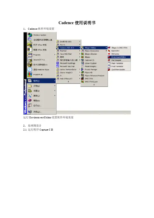
Cadence 使用参考手册邓海飞微电子学研究所设计室20XX7月目录概述11.1 Cadence概述11.2 ASIC设计流程1第一章Cadence 使用基础52.1 Cadence 软件的环境设置52.2 Cadence软件的启动方法102.3库文件的管理122.4文件格式的转化132.5 怎样使用在线帮助132.6 本手册的组成14第二章Verilog-XL 的介绍153. 1 环境设置153.2 Verilog-XL的启动153.3 Verilog-XL的界面173.4 Verilog-XL的使用示例183.5 Verilog-XL的有关帮助文件19第四章电路图设计与电路模拟214.1 电路图设计工具Composer (21)4.1.1 设置214.1.2 启动224.1.3 用户界面与使用方法224.1.4 使用示例244.1.5 相关在线帮助文档244.2 电路模拟工具Analog Artist (24)4.2.1 设置244.2.2 启动254.2.3 用户界面与使用方法254.2.5 相关在线帮助文档25第五章自动布局布线275.1 Cadence中的自动布局布线流程275.2 用AutoAbgen进行自动布局布线库设计28第六章版图设计与其验证306.1 版图设计大师Virtuoso Layout Editor (30)6.1.1 设置306.1.2 启动306.1.3 用户界面与使用方法316.1.4 使用示例316.1.5 相关在线帮助文档326.2 版图验证工具Dracula (32)6.2.1 Dracula使用介绍326.2.2 相关在线帮助文档33第七章skill语言程序设计347.1 skill语言概述347.2 skill语言的基本语法347.3 Skill语言的编程环境347.4面向工具的skill语言编程35附录1 技术文件与显示文件示例60附录2 Verilog-XL实例文件721.Test_memory.v (72)2.SRAM256X8.v (73)3.ram_sy1s_8052 (79)4.TSMC库文件84附录3 Dracula 命令文件359概述作为流行的EDA工具之一,Cadence一直以来都受到了广大EDA工程师的青睐。

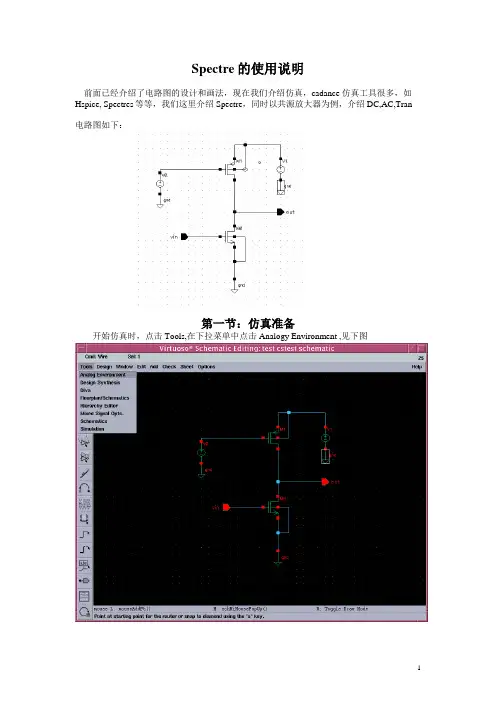
Spectre的使用说明前面已经介绍了电路图的设计和画法,现在我们介绍仿真,cadance 仿真工具很多,如Hspice, Spectres等等,我们这里介绍Spectre,同时以共源放大器为例,介绍DC,AC,Tran电路图如下:第一节:仿真准备开始仿真时,点击Tools,在下拉菜单中点击Analogy Environment ,见下图出现如下窗口1.1 先介绍各条命令及其下拉的子命令的作用:一:Session:菜单包括Schematic Window、Save State、Load State、Options、Reset、Quit 等菜单项。
Schematic window项回到电路图(此时仿真窗口仍存在,只是当前的活动窗口为电路图);Save State项打开相应的窗口,保存当前所设定的模拟所用到的各种。
参数。
如图所示。
窗口中的两项分别为状态名(Save As)和选择需保存的内容(What to Save)。
Load State打开相应的窗口,加载已经保存的状态。
Reset 重置analog artist。
相当于重新打开一个模拟窗口,Quit退出仿真。
二:Setup 菜单包括Design、Simulator/directory/host、Temperature、Model libraries,Stimulition,Simulation Files,Environment等菜单项:1: Design项选择所要模拟的线路图。
2: Simulator/directory/host 项选择模拟使用的模型,点击此项,出现如下图窗点击Simulator项,出现下拉菜单如下图系统提供的选项有cdsSpice、hspiceS、spectreS等等。
我们一般用到的是cdsSpice和spectre,spectreS。
其中采用spectre,spectreS进行的模拟更加精确。
我们使用的上华提供的库,应使用spectre库,下面我们只以这种工具为例说明。
Cadence使用说明书1、 Cadence软件环境设置运行Environment Editor设置软件环境变量2、原理图设计2.1 运行程序Capture CIS在下拉菜单中选择OrCAD Capture CIS option with Capture点击file/new/project…建立原理图工程在Name栏填写工程名称,在Create a New Project Using里面选择Schematic项,在Location 栏中填写工程存放路径。
点击OK后生成工程test,显示如下,PAGE1为自动生成的空原理图文件,右键点击后可以进行rename操作。
2.2 原理图库的构建点击file/new/library在test工程library文件中就会增加一项右键点击.\library1.olb显示如下图所示选择New Part出现对话框:Name表示原件的名称,在原理图设计时用到;Part Reference表示默认的编号名称,如芯片用U表示;PCB Footprint表示该原件的印制板封装;Multiple-Part Package/Parts per表示该原件有几部分组成;选项Pin Number Visible表示引脚数字是否可见;填写修改后点击生成新原件,在虚线框内画上器件符号,然后将虚线框缩小到符号一样大;再运行place/pin添加引脚在Name中填写引脚名称,在Number中填写引脚编号,在Shape下拉菜单中选择引脚外形,在Type下拉菜单中选择引脚类型,要与实际芯片手册一致;Width选项表示是该引脚是总线还是独立信号;一部分编辑完成后,存档,如果该原件由多个部分组成,则点击/view/Next Part,编辑下一部分,直到所有part都编辑完成。
如果一开始定义的part不够多,可以点击Options/Package Properties…修改part的数量。
这样一个原理图库就构建完了。
Cadence和SpectreRF教程⿇省理⼯学院电⽓⼯程与计算机科学系6.776⾼速通信电路2005年春Cadence和SpectreRF教程Albert Jerng02/13/05引⾔本教程将介绍使⽤Cadence和SpectreRF在6.776 课程⾥对电路进⾏仿真。
Cadence包含了IC设计的整个设计流程的所有⼯具,包括电路原理图、版图、电路仿真和验证⼯具。
我们将在⿇省理⼯学院的SUN服务器上运⾏Cadence 4.4.6版本。
Spectre 电路仿真器需要在Cadence的设计框架中的Affirma模拟设计环境下运⾏。
Spectre是⼀种先进的SPICE仿真器,它可以在差分⽅程级进⾏模拟和数字电路的仿真。
SpectreRF 还包括⼀些附加的仿真功能,如周期稳态(PSS)分析,S参数分析及⾮线性噪声分析,这些分析将使射频电路的仿真更加容易。
本教程将⾸先介绍如何在美国⿇省理⼯学院服务器上获得6.776 课程的Cadence运⾏环境。
然后,给出两个例⼦帮助你熟悉SpectreRF电路仿真器。
运⾏Cadence1 登录到⿇省理⼯学院的SUN服务器2 键⼊以下命令⾏:add 6.776source /mit/6.776/setup_cadence你可以添加这些命令⾏到你的.cshrc.mine⽂件,这样你就不必每次重复这⼀步。
如果发⽣改变,你必须键⼊source.cshrc.mine。
3 ⾸次运⾏Cadence时,remove或move你的?/cds⽬录,然后键⼊:CadenceCadence 446 就可以启动了,并且会创建⼀个包含6.776所需⽂件的⽬录?/cds。
这时,你应该会看到icfb和Library Manager这两个视窗,在Library Manager,你会看到以下的之前下载的⽂件夹:6776_Examples , 6776_Primitives , analogLib ,basic6776_Primitives包含我们这节课将会⽤到的NMOS和PMOS晶体管symbols。
麻省理工学院电气工程与计算机科学系6.776高速通信电路2005年春Cadence和SpectreRF教程Albert Jerng02/13/05引言本教程将介绍使用Cadence和SpectreRF在6.776 课程里对电路进行仿真。
Cadence包含了IC设计的整个设计流程的所有工具,包括电路原理图、版图、电路仿真和验证工具。
我们将在麻省理工学院的SUN服务器上运行Cadence 4.4.6版本。
Spectre 电路仿真器需要在Cadence的设计框架中的Affirma模拟设计环境下运行。
Spectre是一种先进的SPICE仿真器,它可以在差分方程级进行模拟和数字电路的仿真。
SpectreRF 还包括一些附加的仿真功能,如周期稳态(PSS)分析,S参数分析及非线性噪声分析,这些分析将使射频电路的仿真更加容易。
本教程将首先介绍如何在美国麻省理工学院服务器上获得6.776 课程的Cadence运行环境。
然后,给出两个例子帮助你熟悉SpectreRF电路仿真器。
运行Cadence1 登录到麻省理工学院的SUN服务器2 键入以下命令行:add 6.776source /mit/6.776/setup_cadence你可以添加这些命令行到你的.cshrc.mine文件,这样你就不必每次重复这一步。
如果发生改变,你必须键入source .cshrc.mine。
3 首次运行Cadence时,remove或move你的〜/cds目录,然后键入:CadenceCadence 446 就可以启动了,并且会创建一个包含6.776所需文件的目录〜/cds。
这时,你应该会看到icfb和Library Manager这两个视窗,在Library Manager,你会看到以下的之前下载的文件夹:6776_Examples , 6776_Primitives , analogLib ,basic6776_Primitives包含我们这节课将会用到的NMOS和PMOS晶体管symbols。
cadence使用教程Cadence是一种电路设计和仿真软件,非常适合电子工程师用于电路设计和分析。
在本教程中,我们将介绍如何使用Cadence进行基本的电路设计和仿真。
首先,打开Cadence软件,并新建一个新项目。
请确保你已经安装了Cadence软件,并且拥有一个有效的许可证。
在新项目中,你需要定义电路的基本参数,如电源电压、电阻值等。
可以通过绘制原理图的方式来完成这些参数的定义。
在绘图界面中,你可以选择不同的元件,包括电源、电阻、电容、电感等。
你可以使用菜单栏中的工具来放置和连接这些元件。
一旦电路图绘制完成,你可以对电路进行仿真。
首先,需要选择合适的仿真器。
Cadence提供了多种仿真器,如Spectre和HSPICE。
选择一个适合你电路的仿真器,并设置仿真参数,如仿真时间、仿真步长等。
在仿真之前,你首先需要对电路进行布局。
布局涉及将电路中的元件放置在芯片上,并根据布线规则进行连接。
Cadence提供了强大的布局工具,可以帮助你完成这个过程。
完成布局后,你可以进行后仿真。
后仿真涉及将布局好的电路导入到仿真器中,并进行仿真分析。
你可以查看电路的性能指标,如电压、电流和功耗等。
除了基本的电路设计和仿真,Cadence还提供了其他功能,如噪声分析、温度分析和优化设计等。
你可以根据需要选择适合的功能。
总的来说,Cadence是一个功能强大的电路设计和仿真软件。
通过本教程,你可以学会如何使用Cadence进行基本的电路设计和仿真。
希望这对你的电子工程项目有所帮助。
麻省理工学院电气工程与计算机科学系6.776高速通信电路2005年春Cadence和SpectreRF教程Albert Jerng02/13/05引言本教程将介绍使用Cadence和SpectreRF在6.776 课程里对电路进行仿真。
Cadence包含了IC设计的整个设计流程的所有工具,包括电路原理图、版图、电路仿真和验证工具。
我们将在麻省理工学院的SUN服务器上运行Cadence 4.4.6版本。
Spectre 电路仿真器需要在Cadence的设计框架中的Affirma模拟设计环境下运行。
Spectre是一种先进的SPICE仿真器,它可以在差分方程级进行模拟和数字电路的仿真。
SpectreRF 还包括一些附加的仿真功能,如周期稳态(PSS)分析,S参数分析及非线性噪声分析,这些分析将使射频电路的仿真更加容易。
本教程将首先介绍如何在美国麻省理工学院服务器上获得6.776 课程的Cadence运行环境。
然后,给出两个例子帮助你熟悉SpectreRF电路仿真器。
运行Cadence1 登录到麻省理工学院的SUN服务器2 键入以下命令行:add 6.776source /mit/6.776/setup_cadence你可以添加这些命令行到你的.cshrc.mine文件,这样你就不必每次重复这一步。
如果发生改变,你必须键入source .cshrc.mine。
3 首次运行Cadence时,remove或move你的〜/cds目录,然后键入:CadenceCadence 446 就可以启动了,并且会创建一个包含6.776所需文件的目录〜/cds。
这时,你应该会看到icfb和Library Manager这两个视窗,在Library Manager,你会看到以下的之前下载的文件夹:6776_Examples , 6776_Primitives , analogLib ,basic6776_Primitives包含我们这节课将会用到的NMOS和PMOS晶体管symbols。
CS/EE 5720/6720 – Analog IC Design Tutorial for Schematic Design and Analysis using Spectre Introduction to Cadence EDA:The Cadence toolset is a complete microchip EDA (Electronic Design Automation) system, which is intended to develop professional, full-scale, mixed-signal microchips. The modules included in the toolset are for schematic entry, design simulation, data analysis, physical layout, and final verification. The Cadence tools at our university are the same as those at most every professional mixed-signal microelectronics company in the United States. The strength of the Cadence tools is in its analog design/simulation/layout and mixed-signal verification and is often used in tandem with other tools for digital design/simulation/layout, where complete top-level verification is done in the Cadence tools.An important concept is that the Cadence tools only provide a framework for doing design. Without a foundry-provided design kit, no design can be done. The design rules used by Cadence set up in this class is based for AMI’s C5N process (0.5 micron 3 metal 2 poly process).So, how is Cadence set up?Broadly, there are three sets of files that need to be in place in order to use Cadence.1)The Cadence toolsThese are the design tools provided by the Cadence company. These tools are located in the /home/cadence directory. They are capable of VLSI integration, project management, circuit simulation, design rule verification, and many other things (most of which we won't use).2)The foundry-based design kitAs mentioned before, the Cadence tools have to be supported by a foundry-baseddesign kit. In this class, we use Cadence design kit developed by the North Carolina State University (NCSU CDK). NCSU CDK provides an environment that has been customized with several technology files and a fair amount of custom SKILL code. These files contain information useful for analog/full-custom digital CMOS IC design via the MOSIS IC fabrication service (). This information includes layer definitions (e.g. colors, patterns, etc.), parasitic capacitances, layout cells, SPICE simulation parameters, Diva rules for Design Rule Check (DRC), extraction, and Layout Versus Schematic (LVS) verification, with various GUI enhancements.For more information on the capability of the NCSU CDK, go to/CDKoverview.htmlThis design kit is located in the /home/cadence/ncsu/local directory. All the design parameters that are needed by the Cadence tools are located in various files in the sub-directories you will find here. The nominal spice parameters for n type transistors for AMI’s 0.5 micron process used in this class can be found in /home/cadence/ncsu/local/models/spectre/nom/ami06N.m.3)The set up files in your local cadence directoryThere are set up files that should be in your local Cadence directory (i.e. the directory from which you invoke Cadence) that sets up the required local environmental variables for Cadence to work on your computer terminal. They are as follows:.cdsinit, .cdsplotinit, .simrc (sets up the variables to be used by NCSU CDK).cdsenv (not essential, but sets your preferences which can be different from userto user)Also we need a .cshrc file to source the current version of cadence we are using in this class.Now, of the three sets of files, the first two sets containing the cadence tools and the NCSU CDK have been already set up by the Cadence Administrators for the class. In this tutorial, the process of setting up the required files in your local cadence directory is explained.Setting up Cadence2000Note: People who have already set up Cadence before still need to follow the steps below.Before you start using cadence you need to complete the following steps:1.First, before anything else, make a directory from which to run Cadence. This isimportant so that all of Cadence’s files end up in a consistent location. I recommend making an IC_CAD directory and then under that making a cadence directory:cdmkdir IC_CADmkdir IC_CAD/cadence2.You need to add the following lines in your .tcshrc file (or whatever shell setupfile you use…) Just open it up with emacs and add:set path = (/uusoc/facility/cad_common/local/bin $path)setenv ICDIR IC_CADsetenv CADENCEDIR $ICDIR/cadencesetenv LOCAL_CADSETUP /uusoc/facility/cad_common/local/class/5830/cadence Adding the first line will update your search path to include the path of the customized CAD tool startup scripts. The next lines set your working directory for cadence as ‘IC_CAD/cadence’. The fourth line sets up the path to a directory that contains class-specific settings. After you save this file you can log out and log in again, or you can source it from the command prompt in the following way.:~> source .tcshrcThe sourcing only needs to be done the first time. After that the .tcshrc file will be sourced automatically when you log in and start up a shell.Starting Cadence 2000 and Making a new Working Library Now that you have your own Cadence directory (called IC_CAD/cadence if you’ve followed the directions up to this point), you need to remember to connect to this directory before you start the Cadence tools. That way Cadence will see the init files that you’ve put in that directory, and find the circuits you’ve designed since all the design files will be stored in this directory. In order to organize your new circuits, you now need to create a new library using the Cadence library manager to hold your design files.1. Connect to your class cadence directory (cd ~/IC_CAD/cadence) and run the command ncsu-icfb (this stands for North Carolina State University and “ic f ront to b ack,” in case you’re curious). You should get a window (called the Command Information Window – CIW) as shown below:2. Library Manager will automatically be opened. If not, in the CIW, select Tools →Library Manager…. You should get the following window, with the following list of libraries:3. In order to build your own schematics, you’ll need to define your own library to keep your own circuits in. To create a new working library in the library manager, select File → New → Library. In the Create Library window that appears fill in the Name field as CSEE5720 (or whatever you’d like to call your library). Select ‘Attach to existing tech library’ for Technology Library. Select “UofU AMI 0.6u C5N” process and press OK.Path field is left blank.NOTE: This may take a few minutes to executeNow the working library has been created. All the project cells (components) that you generate should end up in this library. When you start up the Library Manager to begin working on your circuits, make sure you select your own library to work in. Creating a New CellWhen you create a new cell (component in the library), you actually create a view of the cell. For now we’ll be creating “schematic” views, but eventually you’ll have other different views of the same cell. For example, a “layout” view of the same cell will have the composite layout information in it. It’s a different file, but it should represent the same circuit. This will be discussed later in more details. For now, we’re creating a schematic view. To create a cell view, carry out the following steps:Creating the Schematic View of an RC filter1.Select File → New → Cell View… from the Library Manager menu or tothe CIW menu. The Create New File window appears. The Library Name field is CSEE5720. Fill in the Cell Name field as RC_filter. Choose Composer - Schematic from the Tool list and the view name is automatically filled as Schematic. The library path file is automatically set. Click OK.2. A blank window called Virtuoso Schematic Editing: CSEE5720 RC_filterSchematic appears.3.Adding InstancesAn instance (either a gate from the standard cell library, or a cell that you’ve designed earlier) can be placed in the schematic by selecting Add → Instance…or by pressing ‘i’, and the following Component Browser window appears:4.For this example, we need to add the following components: Capacitor of 1 µFand two resistors of 1kΩ ohm and 10kΩ respectively. To add a capacitor of 1 µF, select the NCSU_Analog_Parts Library and the R_L_C menu. Choose cap in the sub-menu that appears. This opens the Add Instance window:Now, enter the capacitance value of 1u F and hit Hide. Place the capacitor in the schematic window.Other instances can be added in the similar fashion as above. Resistors can be found in R_L_C→ res. Enter the required resistor value.To come out of the instance command mode, press Esc. (This is a good command to know about in general. Whenever you want to exit an editing mode that you’re in, use Esc. I sometimes just hit a bunch of Esc’s whenever I’m not doing something else just to make sure I’m not still in a strange mode from the last command. )5.Connecting Instances with WiresTo connect the different instances with wires we select Add → Wire (narrow) or press “w” to activate the wire command. Now go to the node of the instance and left-click on it to draw the wire and left-click on another node to make theconnection. If you need to end the wire at any point other than a node (i.e. to adda pin later on), double left-click at that point. To come out of the wire commandmode, press Esc.6.Adding PinsPins can be added by going to Add → Pin… or pressing “p”. For example, to put two input pins In& gnd, we can fill in the Pin Names field as In gnd (with a space) and the Direction list as input.Now go to the wire where you need to place the pin and left-click on it.Also, add the output pin ‘Out’ in a similar way.7.Other Command FunctionsSome common command modes and functions available under the Add and Edit menus in cadence are:Under Add Menu:Add → Wire (wide) or press “W” ---------- to add a busAdd → Wire name… or press “l” ---------- to name wiresAdd → Note → Note Text… or press “L” ------------ to add a noteUnder Edit Menu:Edit → Undo or press “u”Edit → Stretch or press “m”Edit → Copy or press “c”Edit → Move or press “M”Edit → Delete or press Delete KeyEdit → Rotate or press “r”Edit → Fit or press “f”There are some command modes and functions available under the Windowmenu also.ing all the commands given above the schematic of a RC_filter can beconstructed as shown below.9.Checking and Saving the DesignThe design can be checked and saved by selecting Design → Check and Save or by pressing “X”. For an error free schematic, you should get the followingmessage in the CIW,Extracting “RC_filter schematic”Schematic check completed with no errors.”CSEE5720 RC_filter schematic” saved.Note: The CIW should not show any warnings or errors when you check and save.10.After saving the design with no errors, select Window → Close.Creating a Symbol View of the RC_filterYou have now created a schematic view of your RC_filter. Now you need to create a symbol view if you want to use that circuit in a different schematic.1.In the Vvirtuoso schematic window of the schematic you have created above,select Design → Create Cell View → From Cell View…. A Cell View from Cell View window appears, press OK.2.In the Virtuoso Symbol Editing window that appears, make modifications tomake the symbol look as below. Replace [@partname] with the name RC_filter and move gnd pin to the bottom side of the cell. You may delete[@instanceName]. Save the symbol and exit using Window → Close.3.Now the RC_filter is ready to be used in other schematics.Analysis using SpectreTo simulate this circuit with an analog simulator, you need to tell the simulator what voltages you’ll be using for your signals. You’ll need to use voltage sources that drive the analog simulation right into the schematic and then simulate the schematic with the analog simulator. In this case, the test fixture is the separate schematic that has the circuit you want to test, and the voltage sources that power it up.Make a new schematic view under the library CSEE5720 and name it RC_filter_test. Choose Add → Instance or press “i” and choose the library - CSEE5720, Menu – uncategorized which will lead to sub-menu RC_filter. Place this in the new schematic editor.We intend to do a transient (time domain), ac (frequency domain) and a dc sweep simulation. Hence we need to add three different types of voltage sources as input to the filter (all stacked up in series as shown below). Of these, only one would be active during each type of simulation; the others would be shorted.1.The input voltage source for transient simulation will be vpulse (taken fromNCSU_Analog_parts library, menu: Voltage_Sources) with the following specifications: this source will generate pulses from 0V to 5V with the givenpulse width and period. Notice that we assign it a finite rise and fall time which means that the change from 0V to 5V (or back) isn’t instant, it takes some time.This is a better model for the analog behavior of the circuit than a pure square wave.Voltage 1 0 vVoltage 2 5 vDelay time 0u sRise time 2u sFall time 2u sPulse Width 5m s10msPeriod2.The input voltage source for AC simulation will be vsin (taken fromNCSU_Analog_parts library, menu: Voltage_Sources) with the AC magnitude set to 1 V.3.The input voltage source for DC simulation will be vdc (taken fromNCSU_Analog_parts library, menu: Voltage_Sources). No other specifications need to be entered, as we will be sweeping this voltage value.4.The ground connection to be selected is gnd (found at NCSU_Analog_partslibrary, menu: Supply_Nets). Note there are a many types of ground connections in the sub-menu. Make sure you only select gnd.5.Connect all the symbols with wires. Add the output pin Out as well as label theinput and output wires (Add → Wire Name or press ‘l’ and place the label on the wire)6.Check and save by selecting Design → Check and Save or by pressing “X”. Ifthere are no errors found, your schematic is ready for Spectre Simulation.Simulation Using Analog EnvironmentIn the Schematic Editor, select Tools → Analog Environment. In the Affirma Analog Circuit Design Environment Simulation Window that appears, there are many kinds of simulators and analysis methods. We have set the default to SpectreS simulation and also have set the corresponding model paths and scaling factor. All you need to do in this window is to select the type of analysis you need and then select the nodes at which you want to observe the waveforms. You are encouraged to play around with the various menus and figure out how they make can your analysis easy and interesting.For transient analysis:On selecting Analyses menu, select tran to perform transient analysis. Transient analysis means that you want to simulate the behavior of the circuit over time, as opposed to a dc operating condition in a steady state or a linearized ac frequency-domain analysis. The stimuli has a period of 10 ms, therefore choose a Stop Time of 20 ms (type 20m in the box) to get a simulation over two complete periods. Click OK.The nodes to be plotted directly after simulation can now be chosen by selecting Outputs → To Be Plotted → Select on Schematic.Select the wires to be plotted (in this case the In and Out voltages of the inverter), by clicking on them in the schematic window. When you click on a wire (the blue line), the voltage is chosen to be plotted, and the wire changes color. To plot currents, you will need to click on the corresponding terminal of an instance and there will be a colored circle around that terminal to indicate a current marker.Now choose Simulation → Run or hit the green traffic lights on the right hand side of the window. The simulation starts. Wait for the simulation to complete. A Waveform Window containing 2 curves on top of each other will be now displayed. To get a betterview of the simulated result, press the switch axis mode-button located on the left side of the waveform window.The following Waveform Window showing the input and output of the inverter is now displayed:Take a moment to explore the features available in the Waveform Window. Use the zoom option (by typing z), and magnify an edge. Measure the time between two points using the A and B markers.For DC sweep of the input:You may first want to delete or disable your previous analysis. This can be done by selecting the analysis that you want to disable/delete and then looking for options under Analyses. You may also disable/delete the IN waveform from being plotted for the ac and dc analyses.Now, choose dc under the Analyses menu. Select ‘Component Parameter’ as the sweep variable. Click on the ‘Select Component’ button and the RC_filter schematic is opened in order to select the sweep variable (You may have to click it twice before the schematic shows up. If you are unable to see the circuit in the schematic editor then select the schematic window and press ‘f’). Select the vdc voltage source. This activates another window as shown below. Select the “DC voltage” option.Now, again select the Analyses menu. It should look like this:Enter the sweep range (0 V to 5 V) and sweep type (Linear with step size 0.1 V) as shown above. Run the simulation.Your output should look something like this:For AC analysis and Bode plots:1.You may want to disable the other analyses first and select only OUTwaveform to be plotted.2.Analyses > Choose > ac > Frequency3.Start-Stop > Start: 1 Stop: 1M4.Sweep Type > Logarithmic 10 points per decade5.Simulation > Run6.You will get a plot of Out vs frequency which looks like the figure below.Note: This is not a conventional Bode plot. We must take 20·log10(out) to get the proper plot.7.In the Waveform Window, select Curves > Edit (select /Out and delete it).8.Now in the Analog Artist Window, select Tools > Calculator > vf (thiswould open the schematic window).9.In the schematic, select Out.10.In the Calculator Window you should get VF(*/Out*).11.Next select dB20.12.In the Calculator Window you should get dB20(VF(*/Out*)).13.Now select plot. You should get a DB plot similar to the one shown below.14.Add the phase by doing Tools > Calculator > vf (this would open theschematic window).15.In the schematic, select Out.16.In the Calc ulator Window you should get VF(*/Out*).17.Next, select phase.18.In the Calculator Window you should get phase(VF(*/Out*)).19.Now select plot. You should get a phase plot similar to the one shown below.21。