MAX485简介
- 格式:doc
- 大小:48.00 KB
- 文档页数:2
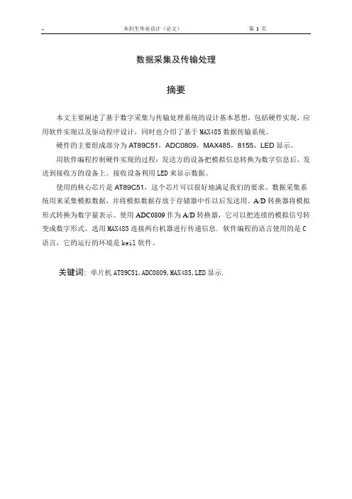
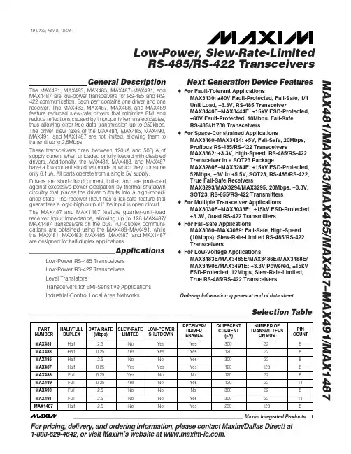
Low-Power, Slew-Rate-Limited RS-485/RS-422 Transceivers2MAX481/MAX483/MAX485/MAX487–MAX491/MAX1487ABSOLUTE MAXIMUM RATINGSSupply Voltage (V CC ) (12V)Control Input Voltage (RE , DE)...................-0.5V to (V CC + 0.5V)Driver Input Voltage (DI).............................-0.5V to (V CC + 0.5V)Driver Output Voltage (A, B)...................................-8V to +12.5VReceiver Input Voltage (A, B).................................-8V to +12.5VReceiver Output Voltage (RO)....................-0.5V to (V CC + 0.5V)Continuous Power Dissipation (T A = +70°C)8-Pin Plastic DIP (derate 9.09mW/°C above +70°C)....727mW14-Pin Plastic DIP (derate 10.00mW/°C above +70°C)..800mW8-Pin SO (derate 5.88mW/°C above +70°C).................471mW 14-Pin SO (derate 8.33mW/°C above +70°C)...............667mW 8-Pin µMAX (derate 4.1mW/°C above +70°C)..............830mW 8-Pin CERDIP (derate 8.00mW/°C above +70°C).........640mW 14-Pin CERDIP (derate 9.09mW/°C above +70°C).......727mW Operating Temperature Ranges MAX4_ _C_ _/MAX1487C_ A...............................0°C to +70°C MAX4__E_ _/MAX1487E_ A.............................-40°C to +85°C MAX4__M_/MAX1487MJA.............................-55°C to +125°C Storage Temperature Range.............................-65°C to +160°C Lead Temperature (soldering, 10sec).............................+300°C DC ELECTRICAL CHARACTERISTICS(V CC = 5V ±5%, T A = T MIN to T MAX , unless otherwise noted.) (Notes 1, 2)Stresses beyond those listed under “Absolute Maximum Ratings” may cause permanent damage to the device. These are stress ratings only, and functional operation of the device at these or any other conditions beyond those indicated in the operational sections of the specifications is not implied. Exposure to absolute maximum rating conditions for extended periods may affect device reliability.V V IN = -7V V IN = 12V V IN = -7V V IN = 12V Input Current (A, B)I IN2V TH k Ω48-7V ≤V CM ≤12V, MAX487/MAX1487R INReceiver Input Resistance -7V ≤V CM ≤12V, all devices exceptMAX487/MAX1487R = 27Ω(RS-485), Figure 40.4V ≤V O ≤2.4VR = 50Ω(RS-422)I O = 4mA, V ID = -200mV I O = -4mA, V ID = 200mV V CM = 0V -7V ≤V CM ≤12V DE, DI, REDE, DI, RE MAX487/MAX1487,DE = 0V, V CC = 0V or 5.25VDE, DI, RE R = 27Ωor 50Ω, Figure 4R = 27Ωor 50Ω, Figure 4R = 27Ωor 50Ω, Figure 4DE = 0V;V CC = 0V or 5.25V,all devices exceptMAX487/MAX1487CONDITIONS k Ω12µA ±1I OZR Three-State (high impedance)Output Current at Receiver V 0.4V OL Receiver Output Low Voltage3.5V OH Receiver Output High VoltagemV 70ΔV TH Receiver Input HysteresisV -0.20.2Receiver Differential ThresholdVoltage-0.2mA 0.25mA -0.81.01.55V OD2Differential Driver Output(with load)V 2V 5V OD1Differential Driver Output (no load)µA ±2I IN1Input Current V 0.8V IL Input Low VoltageV 2.0V IH Input High VoltageV 0.2ΔV OD Change in Magnitude of DriverCommon-Mode Output Voltagefor Complementary Output StatesV 0.2ΔV OD Change in Magnitude of DriverDifferential Output Voltage forComplementary Output StatesV 3V OC Driver Common-Mode OutputVoltageUNITS MIN TYP MAX SYMBOL PARAMETERLow-Power, Slew-Rate-Limited RS-485/RS-422 Transceivers7MAX481/MAX483/MAX485/MAX487–MAX491/MAX1487______________________________________________________________Pin DescriptionFigure 1. MAX481/MAX483/MAX485/MAX487/MAX1487 Pin Configuration and Typical Operating Circuit。
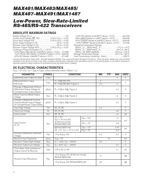
Low-Power, Slew-Rate-Limited RS-485/RS-422 Transceivers12MAX481/MAX483/MAX485/MAX487–MAX491/MAX1487500mV/div 20ns/div ABRO 2V/divV CC = 5V T A = +25°C 500mV/div 20ns/divAB RO2V/divV CC = 5V T A = +25°C500mV/div 400ns/div ABRO2V/div V CC = 5V T A = +25°C 500mV/div 400ns/divA B RO2V/div V CC = 5VT A = +25°CFigure 14. Receiver Propagation Delay Test CircuitFigure 15. MAX481/MAX485/MAX490/MAX491/MAX1487Receiver t PHL Figure 16. MAX481/MAX485/MAX490/MAX491/MAX1487Receiver t PLHPHL Figure 18. MAX483, MAX487–MAX489 Receiver t PLHLow-Power, Slew-Rate-Limited RS-485/RS-422 Transceivers 8MAX481/MAX483/MAX485/MAX487–MAX491/MAX1487__________Applications Information The MAX481/MAX483/MAX485/MAX487–MAX491 and MAX1487 are low-power transceivers for RS-485 and RS-422 communications. The MAX481, MAX485, MAX490,MAX491, and MAX1487 can transmit and receive at data rates up to 2.5Mbps, while the MAX483, MAX487,MAX488, and MAX489 are specified for data rates up to 250kbps. The MAX488–MAX491 are full-duplex trans-ceivers while the MAX481, MAX483, MAX485, MAX487,and MAX1487 are half-duplex. In addition, Driver Enable (DE) and Receiver Enable (RE ) pins are included on the MAX481, MAX483, MAX485, MAX487, MAX489,MAX491, and MAX1487. When disabled, the driver and receiver outputs are high impedance.MAX487/MAX1487:128 Transceivers on the Bus The 48k Ω, 1/4-unit-load receiver input impedance of the MAX487 and MAX1487 allows up to 128 transceivers on a bus, compared to the 1-unit load (12k Ωinput impedance) of standard RS-485 drivers (32 trans-ceivers maximum). Any combination of MAX487/MAX1487 and other RS-485 transceivers with a total of 32 unit loads or less can be put on the bus. The MAX481/MAX483/MAX485 and MAX488–MAX491 have standard 12k ΩReceiver Input impedance.Figure 2. MAX488/MAX490 Pin Configuration and Typical Operating Circuit Figure 3. MAX489/MAX491 Pin Configuration and Typical Operating Circuit。
max485芯片MAX485是一种用于串行通讯的芯片,它可以实现半双工的通信,常用于RS-485网络中。
这款芯片具有低功耗、高速率、低电压、可靠性高等特点,被广泛应用于工业自动化、远程监控、数据采集等领域。
MAX485芯片采用了双绞四线制接口,可以实现长距离传输,通信距离可达1200米。
其通信速率可以高达2.5Mbps,同时还支持多点连接,可以连接最多32个驱动器和接收器。
MAX485芯片的工作电压范围为3.0V至5.25V,因此可以适应不同的工作环境。
在低功耗模式下,它的供电电流仅为1μA,非常适合电池供电的应用。
此外,MAX485还具有过温保护功能,可以保护芯片免受过热损坏。
MAX485芯片的架构采用了低功耗CMOS技术,具有自动接收释放和禁用保护电路,可以有效地降低功耗。
此外,它还配备了过电流保护和过电压保护电路,可以保护芯片免受电路故障的影响。
MAX485芯片的引脚功能如下:- A/B:差分传输线,用于发送和接收数据。
- RE/DE:接收使能/发送使能引脚,用于控制芯片的发送和接收功能。
- RO/RE:发送使能/接收使能引脚,用于选择芯片的发送和接收功能。
- VCC:供电引脚,具有3.0V至5.25V的宽工作电压范围。
- GND:地线引脚,用于接地连接。
MAX485芯片的工作原理如下:- 发送数据时,通过RE/DE引脚将芯片设置为发送模式,将发送的数据信号输入到A/B差分传输线上。
- 接收数据时,通过RE/DE引脚将芯片设置为接收模式,通过RO/RE引脚选择芯片的发送和接收功能。
接收到的数据信号经过差分收发线转换为通用串行总线信号。
- 在半双工通信时,A/B线上只能有一方发送数据,另一方只能接收数据。
总之,MAX485芯片是一款功能强大且灵活的串行通信芯片,具有高速率、低功耗、可靠性高等特点,被广泛应用于工业自动化、远程监控、数据采集等领域。
它的性能优越和稳定性使得它成为RS-485通信领域中的首选芯片。
利用MAX485实现PC机与单片机之间的串行通讯摘要介绍一种RS-485接口芯片MAX485,利用此芯片可以很方便地实现PC机与单片机之间的串行通讯,同时给出PC机与单片机实现多点通讯的实例。
关键词RS-485串行通讯多点通讯随着数据采集系统的广泛应用,通常由单片机构成的应用系统,如仪器仪表、智能设备等,都需要与PC机之间交换数据,实现与PC机之间的通讯功能,以充分发挥PC和单片机之间的功能互补,资源共享的优势。
以往常用的RS-232协议在很大程度上已不能满足设计的要求,如传输速率慢,传输距离短,传输信号易受外界的干扰等缺点。
本文介绍一种性能优越的RS-485接口芯片,以及如何利用此芯片实现单片机与PC机之间的远程通讯,并讨论将其功能进行扩充,实现PC机管理单片机阵列的功能。
1 RS-485协议简介及MAX485芯片介绍由于RS-232的种种缺点,新的串行通讯接口标准RS-449被制定出来,与之相对应的是RS-485的电气标准。
RS-485是美国电气工业联合会(EIA)制定的利用平衡双绞线作传输线的多点通讯标准。
它采用差分信号进行传输;最大传输距离可以达到1.2 km;最大可连接32个驱动器和收发器;接收器最小灵敏度可达±200 mV;最大传输速率可达2.5 Mb/s。
由此可见,RS -485协议正是针对远距离、高灵敏度、多点通讯制定的标准。
MAX485接口芯片是Maxim公司的一种RS-485芯片。
采用单一电源+5 V工作,额定电流为300 μA,采用半双工通讯方式。
它完成将TTL电平与RS-485电平转换的功能。
其引脚结构图如图1所示。
从图中可以看出,MAX485芯片的结构和引脚都非常简单,内部含有一个驱动器和接收器。
RO和DI端分别为接收器的输出和驱动器的输入端,与单片机连接时只需分别与单片机的RXD 和TXD相连即可;/RE和DE端分别为接收和发送的使能端,当/RE为逻辑0时,器件处于接收状态;当DE为逻辑1时,器件处于发送状态,因为MAX485工作在半双工状态,所以只需用单片机的一个管脚控制这两个引脚即可;A端和B端分别为接收和发送的差分信号端,当A引脚的电平高于B 时,代表发送的数据为1;当A的电平低于B端时,代表发送的数据为0。
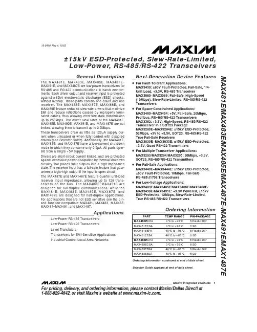
For pricing, delivery, and ordering information,please contact Maxim/Dallas Direct!at 1-888-629-4642, or visit Maxim’s website at .General DescriptionThe MAX481, MAX483, MAX485, MAX487–MAX491, and MAX1487 are low-power transceivers for RS-485 and RS-422 communication. Each part contains one driver and one receiver. The MAX483, MAX487, MAX488, and MAX489feature reduced slew-rate drivers that minimize EMI and reduce reflections caused by improperly terminated cables,thus allowing error-free data transmission up to 250kbps.The driver slew rates of the MAX481, MAX485, MAX490,MAX491, and MAX1487 are not limited, allowing them to transmit up to 2.5Mbps.These transceivers draw between 120µA and 500µA of supply current when unloaded or fully loaded with disabled drivers. Additionally, the MAX481, MAX483, and MAX487have a low-current shutdown mode in which they consume only 0.1µA. All parts operate from a single 5V supply.Drivers are short-circuit current limited and are protected against excessive power dissipation by thermal shutdown circuitry that places the driver outputs into a high-imped-ance state. The receiver input has a fail-safe feature that guarantees a logic-high output if the input is open circuit.The MAX487 and MAX1487 feature quarter-unit-load receiver input impedance, allowing up to 128 MAX487/MAX1487 transceivers on the bus. Full-duplex communi-cations are obtained using the MAX488–MAX491, while the MAX481, MAX483, MAX485, MAX487, and MAX1487are designed for half-duplex applications.________________________ApplicationsLow-Power RS-485 Transceivers Low-Power RS-422 Transceivers Level TranslatorsTransceivers for EMI-Sensitive Applications Industrial-Control Local Area Networks__Next Generation Device Features♦For Fault-Tolerant ApplicationsMAX3430: ±80V Fault-Protected, Fail-Safe, 1/4Unit Load, +3.3V, RS-485 TransceiverMAX3440E–MAX3444E: ±15kV ESD-Protected,±60V Fault-Protected, 10Mbps, Fail-Safe, RS-485/J1708 Transceivers♦For Space-Constrained ApplicationsMAX3460–MAX3464: +5V, Fail-Safe, 20Mbps,Profibus RS-485/RS-422 TransceiversMAX3362: +3.3V, High-Speed, RS-485/RS-422Transceiver in a SOT23 PackageMAX3280E–MAX3284E: ±15kV ESD-Protected,52Mbps, +3V to +5.5V, SOT23, RS-485/RS-422,True Fail-Safe ReceiversMAX3293/MAX3294/MAX3295: 20Mbps, +3.3V,SOT23, RS-855/RS-422 Transmitters ♦For Multiple Transceiver ApplicationsMAX3030E–MAX3033E: ±15kV ESD-Protected,+3.3V, Quad RS-422 Transmitters ♦For Fail-Safe ApplicationsMAX3080–MAX3089: Fail-Safe, High-Speed (10Mbps), Slew-Rate-Limited RS-485/RS-422Transceivers♦For Low-Voltage ApplicationsMAX3483E/MAX3485E/MAX3486E/MAX3488E/MAX3490E/MAX3491E: +3.3V Powered, ±15kV ESD-Protected, 12Mbps, Slew-Rate-Limited,True RS-485/RS-422 TransceiversMAX481/MAX483/MAX485/MAX487–MAX491/MAX1487Low-Power, Slew-Rate-Limited RS-485/RS-422 Transceivers______________________________________________________________Selection Table19-0122; Rev 8; 10/03Ordering Information appears at end of data sheet.M A X 481/M A X 483/M A X 485/M A X 487–M A X 491/M A X 1487Low-Power, Slew-Rate-Limited RS-485/RS-422 Transceivers 2_______________________________________________________________________________________ABSOLUTE MAXIMUM RATINGSSupply Voltage (V CC ).............................................................12V Control Input Voltage (RE , DE)...................-0.5V to (V CC + 0.5V)Driver Input Voltage (DI).............................-0.5V to (V CC + 0.5V)Driver Output Voltage (A, B)...................................-8V to +12.5V Receiver Input Voltage (A, B).................................-8V to +12.5V Receiver Output Voltage (RO).....................-0.5V to (V CC +0.5V)Continuous Power Dissipation (T A = +70°C)8-Pin Plastic DIP (derate 9.09mW/°C above +70°C)....727mW 14-Pin Plastic DIP (derate 10.00mW/°C above +70°C)..800mW 8-Pin SO (derate 5.88mW/°C above +70°C).................471mW14-Pin SO (derate 8.33mW/°C above +70°C)...............667mW 8-Pin µMAX (derate 4.1mW/°C above +70°C)..............830mW 8-Pin CERDIP (derate 8.00mW/°C above +70°C).........640mW 14-Pin CERDIP (derate 9.09mW/°C above +70°C).......727mW Operating Temperature RangesMAX4_ _C_ _/MAX1487C_ A...............................0°C to +70°C MAX4__E_ _/MAX1487E_ A.............................-40°C to +85°C MAX4__MJ_/MAX1487MJA...........................-55°C to +125°C Storage Temperature Range.............................-65°C to +160°C Lead Temperature (soldering, 10sec).............................+300°CDC ELECTRICAL CHARACTERISTICS(V CC = 5V ±5%, T A = T MIN to T MAX , unless otherwise noted.) (Notes 1, 2)Stresses beyond those listed under “Absolute Maximum Ratings” may cause permanent damage to the device. These are stress ratings only, and functional operation of the device at these or any other conditions beyond those indicated in the operational sections of the specifications is not implied. Exposure to absolute maximum rating conditions for extended periods may affect device reliability.V V IN = -7VV IN = 12V V IN = -7V V IN = 12V Input Current (A, B)I IN2V TH k Ω48-7V ≤V CM ≤12V, MAX487/MAX1487R INReceiver Input Resistance -7V ≤V CM ≤12V, all devices except MAX487/MAX1487R = 27Ω(RS-485), Figure 40.4V ≤V O ≤2.4VR = 50Ω(RS-422)I O = 4mA, V ID = -200mV I O = -4mA, V ID = 200mV V CM = 0V-7V ≤V CM ≤12V DE, DI, RE DE, DI, RE MAX487/MAX1487,DE = 0V, V CC = 0V or 5.25VDE, DI, RE R = 27Ωor 50Ω, Figure 4R = 27Ωor 50Ω, Figure 4R = 27Ωor 50Ω, Figure 4DE = 0V;V CC = 0V or 5.25V,all devices except MAX487/MAX1487CONDITIONSk Ω12µA ±1I OZRThree-State (high impedance)Output Current at ReceiverV 0.4V OL Receiver Output Low Voltage 3.5V OH Receiver Output High Voltage mV 70∆V TH Receiver Input Hysteresis V -0.20.2Receiver Differential Threshold Voltage-0.2mA 0.25mA-0.81.01.55V OD2Differential Driver Output (with load)V 2V 5V OD1Differential Driver Output (no load)µA±2I IN1Input CurrentV 0.8V IL Input Low Voltage V 2.0V IH Input High Voltage V 0.2∆V OD Change in Magnitude of Driver Common-Mode Output Voltage for Complementary Output States V 0.2∆V OD Change in Magnitude of Driver Differential Output Voltage for Complementary Output States V 3V OC Driver Common-Mode Output VoltageUNITS MINTYPMAX SYMBOL PARAMETERMAX481/MAX483/MAX485/MAX487–MAX491/MAX1487Low-Power, Slew-Rate-Limited RS-485/RS-422 Transceivers_______________________________________________________________________________________3SWITCHING CHARACTERISTICS—MAX481/MAX485, MAX490/MAX491, MAX1487(V CC = 5V ±5%, T A = T MIN to T MAX , unless otherwise noted.) (Notes 1, 2)DC ELECTRICAL CHARACTERISTICS (continued)(V CC = 5V ±5%, T A = T MIN to T MAX , unless otherwise noted.) (Notes 1, 2)ns 103060t PHLDriver Rise or Fall Time Figures 6 and 8, R DIFF = 54Ω, C L1= C L2= 100pF ns MAX490M, MAX491M MAX490C/E, MAX491C/E2090150MAX481, MAX485, MAX1487MAX490M, MAX491MMAX490C/E, MAX491C/E MAX481, MAX485, MAX1487Figures 6 and 8, R DIFF = 54Ω,C L1= C L2= 100pF MAX481 (Note 5)Figures 5 and 11, C RL = 15pF, S2 closedFigures 5 and 11, C RL = 15pF, S1 closed Figures 5 and 11, C RL = 15pF, S2 closed Figures 5 and 11, C RL = 15pF, S1 closed Figures 6 and 10, R DIFF = 54Ω,C L1= C L2= 100pFFigures 6 and 8,R DIFF = 54Ω,C L1= C L2= 100pF Figures 6 and 10,R DIFF = 54Ω,C L1= C L2= 100pF CONDITIONS ns 510t SKEW ns50200600t SHDNTime to ShutdownMbps 2.5f MAX Maximum Data Rate ns 2050t HZ Receiver Disable Time from High ns 103060t PLH 2050t LZ Receiver Disable Time from Low ns 2050t ZH Driver Input to Output Receiver Enable to Output High ns 2050t ZL Receiver Enable to Output Low 2090200ns ns 134070t HZ t SKD Driver Disable Time from High |t PLH - t PHL |DifferentialReceiver Skewns 4070t LZ Driver Disable Time from Low ns 4070t ZL Driver Enable to Output Low 31540ns51525ns 31540t R , t F 2090200Driver Output Skew to Output t PLH , t PHL Receiver Input to Output4070t ZH Driver Enable to Output High UNITS MIN TYP MAX SYMBOL PARAMETERFigures 7 and 9, C L = 100pF, S2 closed Figures 7 and 9, C L = 100pF, S1 closed Figures 7 and 9, C L = 15pF, S1 closed Figures 7 and 9, C L = 15pF, S2 closedM A X 481/M A X 483/M A X 485/M A X 487–M A X 491/M A X 1487Low-Power, Slew-Rate-Limited RS-485/RS-422 Transceivers 4_______________________________________________________________________________________SWITCHING CHARACTERISTICS—MAX483, MAX487/MAX488/MAX489(V CC = 5V ±5%, T A = T MIN to T MAX , unless otherwise noted.) (Notes 1, 2)SWITCHING CHARACTERISTICS—MAX481/MAX485, MAX490/MAX491, MAX1487 (continued)(V CC = 5V ±5%, T A = T MIN to T MAX , unless otherwise noted.) (Notes 1, 2)3001000Figures 7 and 9, C L = 100pF, S2 closed Figures 7 and 9, C L = 100pF, S1 closed Figures 5 and 11, C L = 15pF, S2 closed,A - B = 2VCONDITIONSns 40100t ZH(SHDN)Driver Enable from Shutdown toOutput High (MAX481)nsFigures 5 and 11, C L = 15pF, S1 closed,B - A = 2Vt ZL(SHDN)Receiver Enable from Shutdownto Output Low (MAX481)ns 40100t ZL(SHDN)Driver Enable from Shutdown toOutput Low (MAX481)ns 3001000t ZH(SHDN)Receiver Enable from Shutdownto Output High (MAX481)UNITS MINTYP MAX SYMBOLPARAMETERt PLH t SKEW Figures 6 and 8, R DIFF = 54Ω,C L1= C L2= 100pFt PHL Figures 6 and 8, R DIFF = 54Ω,C L1= C L2= 100pFDriver Input to Output Driver Output Skew to Output ns 100800ns ns 2000MAX483/MAX487, Figures 7 and 9,C L = 100pF, S2 closedt ZH(SHDN)Driver Enable from Shutdown to Output High2502000ns2500MAX483/MAX487, Figures 5 and 11,C L = 15pF, S1 closedt ZL(SHDN)Receiver Enable from Shutdown to Output Lowns 2500MAX483/MAX487, Figures 5 and 11,C L = 15pF, S2 closedt ZH(SHDN)Receiver Enable from Shutdown to Output Highns 2000MAX483/MAX487, Figures 7 and 9,C L = 100pF, S1 closedt ZL(SHDN)Driver Enable from Shutdown to Output Lowns 50200600MAX483/MAX487 (Note 5) t SHDN Time to Shutdownt PHL t PLH , t PHL < 50% of data period Figures 5 and 11, C RL = 15pF, S2 closed Figures 5 and 11, C RL = 15pF, S1 closed Figures 5 and 11, C RL = 15pF, S2 closed Figures 5 and 11, C RL = 15pF, S1 closed Figures 7 and 9, C L = 15pF, S2 closed Figures 6 and 10, R DIFF = 54Ω,C L1= C L2= 100pFFigures 7 and 9, C L = 15pF, S1 closed Figures 7 and 9, C L = 100pF, S1 closed Figures 7 and 9, C L = 100pF, S2 closed CONDITIONSkbps 250f MAX 2508002000Maximum Data Rate ns 2050t HZ Receiver Disable Time from High ns 25080020002050t LZ Receiver Disable Time from Low ns 2050t ZH Receiver Enable to Output High ns 2050t ZL Receiver Enable to Output Low ns ns 1003003000t HZ t SKD Driver Disable Time from High I t PLH - t PHL I DifferentialReceiver SkewFigures 6 and 10, R DIFF = 54Ω,C L1= C L2= 100pFns 3003000t LZ Driver Disable Time from Low ns 2502000t ZL Driver Enable to Output Low ns Figures 6 and 8, R DIFF = 54Ω,C L1= C L2= 100pFns 2502000t R , t F 2502000Driver Rise or Fall Time ns t PLH Receiver Input to Output2502000t ZH Driver Enable to Output High UNITS MIN TYP MAX SYMBOL PARAMETERMAX481/MAX483/MAX485/MAX487–MAX491/MAX1487Low-Power, Slew-Rate-Limited RS-485/RS-422 Transceivers_______________________________________________________________________________________530002.5OUTPUT CURRENT vs.RECEIVER OUTPUT LOW VOLTAGE525M A X 481-01OUTPUT LOW VOLTAGE (V)O U T P U T C U R R E N T (m A )1.515100.51.02.0203540450.90.1-50-252575RECEIVER OUTPUT LOW VOLTAGE vs.TEMPERATURE0.30.7TEMPERATURE (°C)O U T P U TL O W V O L T A G E (V )500.50.80.20.60.40100125-20-41.5 2.0 3.0 5.0OUTPUT CURRENT vs.RECEIVER OUTPUT HIGH VOLTAGE-8-16M A X 481-02OUTPUT HIGH VOLTAGE (V)O U T P U T C U R R E N T (m A )2.5 4.0-12-18-6-14-10-203.54.5 4.83.2-50-252575RECEIVER OUTPUT HIGH VOLTAGE vs.TEMPERATURE3.64.4TEMPERATURE (°C)O U T P UT H I G H V O L T A G E (V )0504.04.63.44.23.83.01001259000 1.0 3.0 4.5DRIVER OUTPUT CURRENT vs.DIFFERENTIAL OUTPUT VOLTAGE1070M A X 481-05DIFFERENTIAL OUTPUT VOLTAGE (V)O U T P U T C U R R E N T (m A )2.0 4.05030806040200.5 1.5 2.53.5 2.31.5-50-2525125DRIVER DIFFERENTIAL OUTPUT VOLTAGEvs. TEMPERATURE1.72.1TEMPERATURE (°C)D I F FE R E N T I A L O U T P U T V O L T A G E (V )751.92.21.62.01.8100502.4__________________________________________Typical Operating Characteristics(V CC = 5V, T A = +25°C, unless otherwise noted.)NOTES FOR ELECTRICAL/SWITCHING CHARACTERISTICSNote 1:All currents into device pins are positive; all currents out of device pins are negative. All voltages are referenced to deviceground unless otherwise specified.Note 2:All typical specifications are given for V CC = 5V and T A = +25°C.Note 3:Supply current specification is valid for loaded transmitters when DE = 0V.Note 4:Applies to peak current. See Typical Operating Characteristics.Note 5:The MAX481/MAX483/MAX487 are put into shutdown by bringing RE high and DE low. If the inputs are in this state for lessthan 50ns, the parts are guaranteed not to enter shutdown. If the inputs are in this state for at least 600ns, the parts are guaranteed to have entered shutdown. See Low-Power Shutdown Mode section.M A X 481/M A X 483/M A X 485/M A X 487–M A X 491/M A X 1487Low-Power, Slew-Rate-Limited RS-485/RS-422 Transceivers 6___________________________________________________________________________________________________________________Typical Operating Characteristics (continued)(V CC = 5V, T A = +25°C, unless otherwise noted.)120008OUTPUT CURRENT vs.DRIVER OUTPUT LOW VOLTAGE20100M A X 481-07OUTPUT LOW VOLTAGE (V)O U T P U T C U R R E N T (m A )6604024801012140-1200-7-5-15OUTPUT CURRENT vs.DRIVER OUTPUT HIGH VOLTAGE-20-80M A X 481-08OUTPUT HIGH VOLTAGE (V)O U T P U T C U R R E N T (m A )-31-603-6-4-2024-100-40100-40-60-2040100120MAX1487SUPPLY CURRENT vs. TEMPERATURE300TEMPERATURE (°C)S U P P L Y C U R R E N T (µA )20608050020060040000140100-50-2550100MAX481/MAX485/MAX490/MAX491SUPPLY CURRENT vs. TEMPERATURE300TEMPERATURE (°C)S U P P L Y C U R R E N T (µA )257550020060040000125100-50-2550100MAX483/MAX487–MAX489SUPPLY CURRENT vs. TEMPERATURE300TEMPERATURE (°C)S U P P L Y C U R R E N T (µA )257550020060040000125MAX481/MAX483/MAX485/MAX487–MAX491/MAX1487Low-Power, Slew-Rate-Limited RS-485/RS-422 Transceivers_______________________________________________________________________________________7______________________________________________________________Pin DescriptionFigure 1. MAX481/MAX483/MAX485/MAX487/MAX1487 Pin Configuration and Typical Operating CircuitM A X 481/M A X 483/M A X 485/M A X 487–M A X 491/M A X 1487__________Applications InformationThe MAX481/MAX483/MAX485/MAX487–MAX491 and MAX1487 are low-power transceivers for RS-485 and RS-422 communications. The MAX481, MAX485, MAX490,MAX491, and MAX1487 can transmit and receive at data rates up to 2.5Mbps, while the MAX483, MAX487,MAX488, and MAX489 are specified for data rates up to 250kbps. The MAX488–MAX491 are full-duplex trans-ceivers while the MAX481, MAX483, MAX485, MAX487,and MAX1487 are half-duplex. In addition, Driver Enable (DE) and Receiver Enable (RE) pins are included on the MAX481, MAX483, MAX485, MAX487, MAX489,MAX491, and MAX1487. When disabled, the driver and receiver outputs are high impedance.MAX487/MAX1487:128 Transceivers on the BusThe 48k Ω, 1/4-unit-load receiver input impedance of the MAX487 and MAX1487 allows up to 128 transceivers on a bus, compared to the 1-unit load (12k Ωinput impedance) of standard RS-485 drivers (32 trans-ceivers maximum). Any combination of MAX487/MAX1487 and other RS-485 transceivers with a total of 32 unit loads or less can be put on the bus. The MAX481/MAX483/MAX485 and MAX488–MAX491 have standard 12k ΩReceiver Input impedance.Low-Power, Slew-Rate-Limited RS-485/RS-422 Transceivers 8_______________________________________________________________________________________Figure 2. MAX488/MAX490 Pin Configuration and Typical Operating CircuitFigure 3. MAX489/MAX491 Pin Configuration and Typical Operating CircuitMAX483/MAX487/MAX488/MAX489:Reduced EMI and ReflectionsThe MAX483 and MAX487–MAX489 are slew-rate limit-ed, minimizing EMI and reducing reflections caused by improperly terminated cables. Figure 12 shows the dri-ver output waveform and its Fourier analysis of a 150kHz signal transmitted by a MAX481, MAX485,MAX490, MAX491, or MAX1487. High-frequency har-monics with large amplitudes are evident. Figure 13shows the same information displayed for a MAX483,MAX487, MAX488, or MAX489 transmitting under the same conditions. Figure 13’s high-frequency harmonics have much lower amplitudes, and the potential for EMI is significantly reduced.MAX481/MAX483/MAX485/MAX487–MAX491/MAX1487Low-Power, Slew-Rate-Limited RS-485/RS-422 Transceivers_______________________________________________________________________________________9_________________________________________________________________Test CircuitsFigure 4. Driver DC Test Load Figure 5. Receiver Timing Test LoadFigure 6. Driver/Receiver Timing Test Circuit Figure 7. Driver Timing Test LoadM A X 481/M A X 483/M A X 485/M A X 487–M A X 491/M A X 1487Low-Power, Slew-Rate-Limited RS-485/RS-422 Transceivers 10_______________________________________________________Switching Waveforms_________________Function Tables (MAX481/MAX483/MAX485/MAX487/MAX1487)Figure 8. Driver Propagation DelaysFigure 9. Driver Enable and Disable Times (except MAX488 and MAX490)Figure 10. Receiver Propagation DelaysFigure 11. Receiver Enable and Disable Times (except MAX488and MAX490)Table 1. TransmittingTable 2. ReceivingLow-Power Shutdown Mode (MAX481/MAX483/MAX487)A low-power shutdown mode is initiated by bringing both RE high and DE low. The devices will not shut down unless both the driver and receiver are disabled.In shutdown, the devices typically draw only 0.1µA of supply current.RE and DE may be driven simultaneously; the parts are guaranteed not to enter shutdown if RE is high and DE is low for less than 50ns. If the inputs are in this state for at least 600ns, the parts are guaranteed to enter shutdown.For the MAX481, MAX483, and MAX487, the t ZH and t ZL enable times assume the part was not in the low-power shutdown state (the MAX485/MAX488–MAX491and MAX1487 can not be shut down). The t ZH(SHDN)and t ZL(SHDN)enable times assume the parts were shut down (see Electrical Characteristics ).It takes the drivers and receivers longer to become enabled from the low-power shutdown state (t ZH(SHDN ), t ZL(SHDN)) than from the operating mode (t ZH , t ZL ). (The parts are in operating mode if the –R —E –,DE inputs equal a logical 0,1 or 1,1 or 0, 0.)Driver Output ProtectionExcessive output current and power dissipation caused by faults or by bus contention are prevented by two mechanisms. A foldback current limit on the output stage provides immediate protection against short cir-cuits over the whole common-mode voltage range (see Typical Operating Characteristics ). In addition, a ther-mal shutdown circuit forces the driver outputs into a high-impedance state if the die temperature rises excessively.Propagation DelayMany digital encoding schemes depend on the differ-ence between the driver and receiver propagation delay times. Typical propagation delays are shown in Figures 15–18 using Figure 14’s test circuit.The difference in receiver delay times, | t PLH - t PHL |, is typically under 13ns for the MAX481, MAX485,MAX490, MAX491, and MAX1487 and is typically less than 100ns for the MAX483 and MAX487–MAX489.The driver skew times are typically 5ns (10ns max) for the MAX481, MAX485, MAX490, MAX491, and MAX1487, and are typically 100ns (800ns max) for the MAX483 and MAX487–MAX489.MAX481/MAX483/MAX485/MAX487–MAX491/MAX1487Low-Power, Slew-Rate-Limited RS-485/RS-422 Transceivers______________________________________________________________________________________1110dB/div0Hz5MHz500kHz/div10dB/div0Hz5MHz500kHz/divFigure 12. Driver Output Waveform and FFT Plot of MAX481/MAX485/MAX490/MAX491/MAX1487 Transmitting a 150kHz SignalFigure 13. Driver Output Waveform and FFT Plot of MAX483/MAX487–MAX489 Transmitting a 150kHz SignalM A X 481/M A X 483/M A X 485/M A X 487–M A X 491/M A X 1487Low-Power, Slew-Rate-Limited RS-485/RS-422 Transceivers 12______________________________________________________________________________________V CC = 5V T A = +25°CV CC = 5V T A = +25°CV CC = 5V T A = +25°CV CC = 5V T A = +25°CFigure 14. Receiver Propagation Delay Test CircuitFigure 15. MAX481/MAX485/MAX490/MAX491/MAX1487Receiver t PHLFigure 16. MAX481/MAX485/MAX490/MAX491/MAX1487Receiver t PLHPHL Figure 18. MAX483, MAX487–MAX489 Receiver t PLHLine Length vs. Data RateThe RS-485/RS-422 standard covers line lengths up to 4000 feet. For line lengths greater than 4000 feet, see Figure 23.Figures 19 and 20 show the system differential voltage for the parts driving 4000 feet of 26AWG twisted-pair wire at 110kHz into 120Ωloads.Typical ApplicationsThe MAX481, MAX483, MAX485, MAX487–MAX491, and MAX1487 transceivers are designed for bidirectional data communications on multipoint bus transmission lines.Figures 21 and 22 show typical network applications circuits. These parts can also be used as line repeaters, with cable lengths longer than 4000 feet, as shown in Figure 23.To minimize reflections, the line should be terminated at both ends in its characteristic impedance, and stub lengths off the main line should be kept as short as possi-ble. The slew-rate-limited MAX483 and MAX487–MAX489are more tolerant of imperfect termination.MAX481/MAX483/MAX485/MAX487–MAX491/MAX1487Low-Power, Slew-Rate-Limited RS-485/RS-422 Transceivers______________________________________________________________________________________13DIV Y -V ZRO5V 0V1V0V -1V5V 0V2µs/divFigure 19. MAX481/MAX485/MAX490/MAX491/MAX1487 System Differential Voltage at 110kHz Driving 4000ft of Cable Figure 20. MAX483, MAX487–MAX489 System Differential Voltage at 110kHz Driving 4000ft of CableFigure 21. MAX481/MAX483/MAX485/MAX487/MAX1487 Typical Half-Duplex RS-485 NetworkM A X 481/M A X 483/M A X 485/M A X 487–M A X 491/M A X 1487Low-Power, Slew-Rate-Limited RS-485/RS-422 Transceivers 14______________________________________________________________________________________Figure 22. MAX488–MAX491 Full-Duplex RS-485 NetworkFigure 23. Line Repeater for MAX488–MAX491Isolated RS-485For isolated RS-485 applications, see the MAX253 and MAX1480 data sheets.MAX481/MAX483/MAX485/MAX487–MAX491/MAX1487Low-Power, Slew-Rate-Limited RS-485/RS-422 Transceivers______________________________________________________________________________________15_______________Ordering Information_________________Chip TopographiesMAX481/MAX483/MAX485/MAX487/MAX1487N.C. RO 0.054"(1.372mm)0.080"(2.032mm)DE DIGND B N.C.V CCARE * Contact factory for dice specifications.__Ordering Information (continued)M A X 481/M A X 483/M A X 485/M A X 487–M A X 491/M A X 1487Low-Power, Slew-Rate-Limited RS-485/RS-422 Transceivers 16______________________________________________________________________________________TRANSISTOR COUNT: 248SUBSTRATE CONNECTED TO GNDMAX488/MAX490B RO 0.054"(1.372mm)0.080"(2.032mm)N.C. DIGND Z A V CCYN.C._____________________________________________Chip Topographies (continued)MAX489/MAX491B RO 0.054"(1.372mm)0.080"(2.032mm)DE DIGND Z A V CCYREMAX481/MAX483/MAX485/MAX487–MAX491/MAX1487Low-Power, Slew-Rate-Limited RS-485/RS-422 Transceivers______________________________________________________________________________________17Package Information(The package drawing(s) in this data sheet may not reflect the most current specifications. For the latest package outline information go to /packages .)S O I C N .E P SM A X 481/M A X 483/M A X 485/M A X 487–M A X 491/M A X 1487Low-Power, Slew-Rate-Limited RS-485/RS-422 Transceivers 18______________________________________________________________________________________Package Information (continued)(The package drawing(s) in this data sheet may not reflect the most current specifications. For the latest package outline information go to /packages .)MAX481/MAX483/MAX485/MAX487–MAX491Low-Power, Slew-Rate-Limited RS-485/RS-422 TransceiversMaxim cannot assume responsibility for use of any circuitry other than circuitry entirely embodied in a Maxim product. No circuit patent licenses are implied. Maxim reserves the right to change the circuitry and specifications without notice at any time.Maxim Integrated Products, 120 San Gabriel Drive, Sunnyvale, CA 94086 408-737-7600 ____________________19©2003 Maxim Integrated ProductsPrinted USAis a registered trademark of Maxim Integrated Products.M A X 481/M A X 483/M A X 485/M A X 487–M A X 491/M A X 1487P D I P N .E PSPackage Information (continued)(The package drawing(s) in this data sheet may not reflect the most current specifications. For the latest package outline information go to /packages .)。
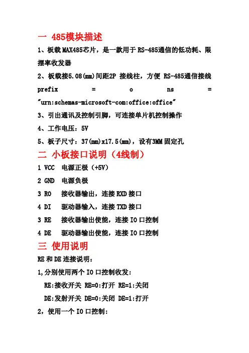
一 485模块描述
1、板载MAX485芯片,是一款用于RS-485通信的低功耗、限摆率收发器
2、板载接5.08(mm)间距2P接线柱,方便RS-485通信接线prefix = o ns = "urn:schemas-microsoft-com:office:office"
3、引出通讯及控制引脚,可连接单片机控制操作
4、工作电压:5V
5、板子尺寸:37(mm)x17.5(mm),设有3MM固定孔
二小板接口说明(4线制)
1 VCC 电源正极(+5V)
2 GND 电源负极
3 RO 接收器输出,连接RXD接口
4 DI 驱动器输入,连接TXD接口
3 RE 接收器输出使能,连接IO口控制
4 DE 驱动器输出使能,连接IO口控制
三使用说明
RE和DE连接说明:
1,分别使用两个IO口控制收发:
RE:接收开关 RE=0:打开 RE=1:关闭
DE:发射开关 DE=0:关闭 DE=1:打开
2,使用一个IO口控制:
RE和DE相连接至一个IO口,IO=0:只接收,IO=1:只发射参考图如下:
两种控制方式取决于系统的设计
3,如果你的系统只有RXD和TXD信号而无控制IO口,则可以由外部直接打开使能,但注意,只能做发射器或接收器。
因板带上拉电阻,RE和DE不连接时(悬空)为高电平,即只做发射器,如需改为接收器使用,则将RE和DE接低电平(接GND端)。
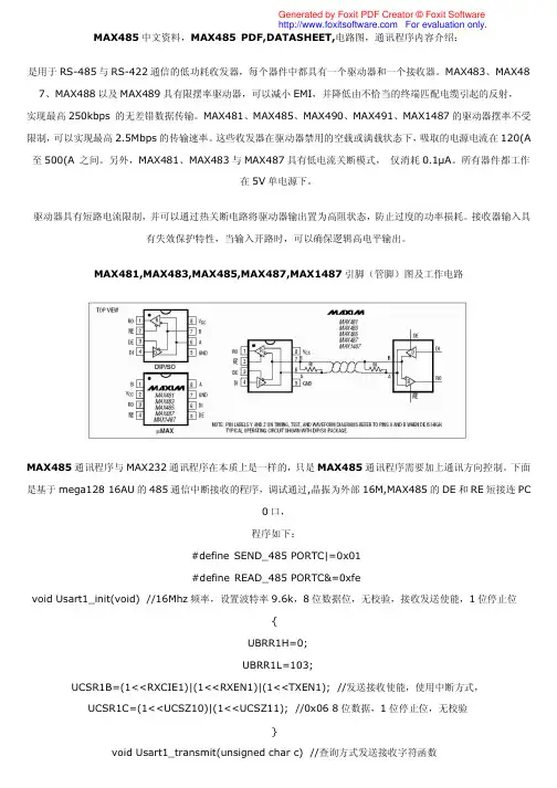
0 MAX485是芯片接口的一种类型。
MAX485接口芯片是Maxim公司的一种RS-485芯片。
MAX485CPAMAX485、MAX487-MAX491以及MAX1487是用于RS-485与RS-422通信的低功耗收发器,每个器件中都具有一个驱动器和一个接收器。
MAX483、MAX487、MAX488以及MAX489具有限摆率驱动器,可以减小EMI,并降低由不恰当的终端匹配电缆引起的反射,实现最高250kbps的无差错数据传输。
MAX481、MAX485、MAX490、MAX491、MAX1487的驱动器摆率不受限制,可以实现最高2.5Mbps 的传输速率。
这些收发器在驱动器禁用的空载或满载状态下,吸取的电源电流在120µA至500µA之间。
另外,MAX481、MAX483与MAX487具有低电流关断模式,仅消耗0.1µA。
所有器件都工作在5V单电源下。
采用单一电源+5 V工作,额定电流为300 μA,采用半双工通讯方式。
它完成将TTL电平转换为RS-485电平的功能。
MAX485芯片的结构和引脚都非常简单,内部含有一个驱动器和接收器。
RO 和DI端分别为接收器的输出和驱动器的输入端,与单片机连接时只需分别与单片机的RXD和TXD相连即可;/RE和DE端分别为接收和发送的使能端,当/RE为逻辑0时,器件处于接收状态;当DE为逻辑1时,器件处于发送状态,因为MAX485工作在半双工状态,所以只需用单片机的一个管脚控制这两个引脚即可;A端和B端分别为接收和发送的差分信号端,当A引脚的电平高于B 时,代表发送的数据为1;当A的电平低于B端时,代表发送的数据为0。
在与单片机连接时接线非常简单。
只需要一个信号控制MAX485的接收和发送即可。
同时将A和B端之间加匹配电阻,一般可选100Ω的电阻。
引脚(管脚)图及工作电路计算机是不能直接识别RS485通讯信号的。
9 RS-485总线扩展
RS-485标准接口是单片机系统种常用的一种串行总线之一。
与RS-232C比较,其性能有许多改进,细节请见表9.1所示。
表9.1 RS-232C与RS-485性能比较
RS-485接口可连接成半双工和全双工两种通信方式。
常见的半双工通信芯片有MAX481、MAX483、MAX485、MAX487等,全双工通信芯片有MAX488、MAX489、MAX490、MAX491等。
下面以MAX485为例来介绍RS-485串行接口的应用。
MAX485的封装有DIP、SO和uMAX三种,其中DIP封装的管脚如图9.1所示。
管脚的功能如下:
RO:接收器输出端。
若A比B大200mV,RO为高;反之为低电平。
RE:接收器输出使能端。
RE为低时,RO有效;为高时,RO呈高阻状态。
DE:驱动器输出使能端。
若DE=1,驱动器输
出A和B有效;若DE=0,则它们呈高阻态。
若
驱动器输出有效,器件作为线驱动器用,反之
作为线接收器用。
DI:驱动器输入端。
DI=0,有A=0,B=1;
当DI=1,则A=1,B=0。
GND:接地。
A:同相接收器输入和同相驱动器输出。
B:反相接收器输入和反相驱动器输出。
VCC:电源端,一般接+5V。
图9.1 MAX485芯片的DIP封装管脚图
MAX485典型的工作电路如图9.2所示,其中平衡电阻Rp 通常取100~300欧姆。
MAX485的收发功能见表9.3。
表9.3 MAX485的收发功能。
max485芯片工作原理
MAX485是一种常用的RS通信接口芯片,可以实现半双工的串行通信。
它的工作原理如下:
1. 驱动器模式:当MAX485处于驱动器模式时,将串行数据输入到芯片的DI(Data Input)引脚,然后芯片内部的驱动器将输入的数据转换成差分信号输出到A与B引,A引脚输出高485处于接收器模式时,A与B上的差分信号将被接收到RE(Receive Enable)引脚控制的接收器输入端。
RE引脚为高电平时,芯片处于接收器模式,此时差分信号经过放大后输出到RO(Receive Output)引脚上。
反之,RE引脚为低电平时,芯片处于驱动器模式,RO引脚将悬空或输出高阻抗。
2. 差分传输:MAX485采用差分传输方式,在传输线上通过比较A与B引脚上的电平差异来接收数据。
高电平差分信号表示逻辑1,低电平差分信号表示逻辑0。
这种差分传输方式具有抗干扰能力强的特点,可以有效减少信号传输中的噪音干扰。
综上所述,MAX485通过驱动器模式和接收器模式的切换,实现了RS485通信的半工功能。
Low-Power, Slew-Rate-Limited RS-485/RS-422 Transceivers2MAX481/MAX483/MAX485/MAX487–MAX491/MAX1487ABSOLUTE MAXIMUM RATINGSSupply Voltage (V CC ) (12V)Control Input Voltage (RE , DE)...................-0.5V to (V CC + 0.5V)Driver Input Voltage (DI).............................-0.5V to (V CC + 0.5V)Driver Output Voltage (A, B)...................................-8V to +12.5VReceiver Input Voltage (A, B).................................-8V to +12.5VReceiver Output Voltage (RO)....................-0.5V to (V CC + 0.5V)Continuous Power Dissipation (T A = +70°C)8-Pin Plastic DIP (derate 9.09mW/°C above +70°C)....727mW14-Pin Plastic DIP (derate 10.00mW/°C above +70°C)..800mW8-Pin SO (derate 5.88mW/°C above +70°C).................471mW 14-Pin SO (derate 8.33mW/°C above +70°C)...............667mW 8-Pin µMAX (derate 4.1mW/°C above +70°C)..............830mW 8-Pin CERDIP (derate 8.00mW/°C above +70°C).........640mW 14-Pin CERDIP (derate 9.09mW/°C above +70°C).......727mW Operating Temperature Ranges MAX4_ _C_ _/MAX1487C_ A...............................0°C to +70°C MAX4__E_ _/MAX1487E_ A.............................-40°C to +85°C MAX4__M_/MAX1487MJA.............................-55°C to +125°C Storage Temperature Range.............................-65°C to +160°C Lead Temperature (soldering, 10sec).............................+300°C DC ELECTRICAL CHARACTERISTICS(V CC = 5V ±5%, T A = T MIN to T MAX , unless otherwise noted.) (Notes 1, 2)Stresses beyond those listed under “Absolute Maximum Ratings” may cause permanent damage to the device. These are stress ratings only, and functional operation of the device at these or any other conditions beyond those indicated in the operational sections of the specifications is not implied. Exposure to absolute maximum rating conditions for extended periods may affect device reliability.V V IN = -7V V IN = 12V V IN = -7V V IN = 12V Input Current (A, B)I IN2V TH k Ω48-7V ≤V CM ≤12V, MAX487/MAX1487R INReceiver Input Resistance -7V ≤V CM ≤12V, all devices exceptMAX487/MAX1487R = 27Ω(RS-485), Figure 40.4V ≤V O ≤2.4VR = 50Ω(RS-422)I O = 4mA, V ID = -200mV I O = -4mA, V ID = 200mV V CM = 0V -7V ≤V CM ≤12V DE, DI, REDE, DI, RE MAX487/MAX1487,DE = 0V, V CC = 0V or 5.25VDE, DI, RE R = 27Ωor 50Ω, Figure 4R = 27Ωor 50Ω, Figure 4R = 27Ωor 50Ω, Figure 4DE = 0V;V CC = 0V or 5.25V,all devices exceptMAX487/MAX1487CONDITIONS k Ω12µA ±1I OZR Three-State (high impedance)Output Current at Receiver V 0.4V OL Receiver Output Low Voltage3.5V OH Receiver Output High VoltagemV 70ΔV TH Receiver Input HysteresisV -0.20.2Receiver Differential ThresholdVoltage-0.2mA 0.25mA -0.81.01.55V OD2Differential Driver Output(with load)V 2V 5V OD1Differential Driver Output (no load)µA ±2I IN1Input Current V 0.8V IL Input Low VoltageV 2.0V IH Input High VoltageV 0.2ΔV OD Change in Magnitude of DriverCommon-Mode Output Voltagefor Complementary Output StatesV 0.2ΔV OD Change in Magnitude of DriverDifferential Output Voltage forComplementary Output StatesV 3V OC Driver Common-Mode OutputVoltageUNITS MIN TYP MAX SYMBOL PARAMETERGeneral DescriptionThe MAX481, MAX483, MAX485, MAX487–MAX491, andMAX1487 are low-power transceivers for RS-485 and RS-422 communication. Each part contains one driver and onereceiver. The MAX483, MAX487, MAX488, and MAX489feature reduced slew-rate drivers that minimize E MI andreduce reflections caused by improperly terminated cables,thus allowing error-free data transmission up to 250kbps.The driver slew rates of the MAX481, MAX485, MAX490,MAX491, and MAX1487 are not limited, allowing them totransmit up to 2.5Mbps.These transceivers draw between 120µA and 500µA ofsupply current when unloaded or fully loaded with disableddrivers. Additionally, the MAX481, MAX483, and MAX487have a low-current shutdown mode in which they consumeonly 0.1µA. All parts operate from a single 5V supply.Drivers are short-circuit current limited and are protectedagainst excessive power dissipation by thermal shutdowncircuitry that places the driver outputs into a high-imped-ance state. The receiver input has a fail-safe feature thatguarantees a logic-high output if the input is open circuit.The MAX487 and MAX1487 feature quarter-unit-loadreceiver input impedance, allowing up to 128 MAX487/MAX1487 transceivers on the bus. Full-duplex communi-cations are obtained using the MAX488–MAX491, whilethe MAX481, MAX483, MAX485, MAX487, and MAX1487are designed for half-duplex applications.________________________Applications Low-Power RS-485 Transceivers Low-Power RS-422 Transceivers Level Translators Transceivers for EMI-Sensitive Applications Industrial-Control Local Area Networks__Next Generation Device Features o For Fault-Tolerant Applications MAX3430: ±80V Fault-Protected, Fail-Safe, 1/4Unit Load, +3.3V, RS-485 Transceiver MAX3440E–MAX3444E: ±15kV ESD-Protected,±60V Fault-Protected, 10Mbps, Fail-Safe, RS-485/J1708 Transceivers o For Space-Constrained Applications MAX3460–MAX3464: +5V, Fail-Safe, 20Mbps,Profibus RS-485/RS-422 Transceivers MAX3362: +3.3V, High-Speed, RS-485/RS-422Transceiver in a SOT23 Package MAX3280E–MAX3284E: ±15kV ESD-Protected,52Mbps, +3V to +5.5V, SOT23, RS-485/RS-422,True Fail-Safe Receivers MAX3293/MAX3294/MAX3295: 20Mbps, +3.3V,SOT23, RS-485/RS-422 Transmitters o For Multiple Transceiver Applications MAX3030E–MAX3033E: ±15kV ESD-Protected,+3.3V, Quad RS-422 Transmitters o For Fail-Safe Applications MAX3080–MAX3089: Fail-Safe, High-Speed (10Mbps), Slew-Rate-Limited RS-485/RS-422Transceiverso For Low-Voltage ApplicationsMAX3483E/MAX3485E/MAX3486E/MAX3488E/MAX3490E/MAX3491E: +3.3V Powered, ±15kVESD-Protected, 12Mbps, Slew-Rate-Limited,True RS-485/RS-422 TransceiversMAX481/MAX483/MAX485/MAX487–MAX491/MAX1487Low-Power, Slew-Rate-Limited RS-485/RS-422 Transceivers ______________________________________________________________Selection Table 19-0122; Rev 10; 9/14PARTNUMBERHALF/FULL DUPLEX DATA RATE (Mbps) SLEW-RATE LIMITED LOW-POWER SHUTDOWN RECEIVER/DRIVER ENABLE QUIESCENT CURRENT (μA) NUMBER OF RECEIVERS ON BUS PIN COUNT MAX481Half 2.5No Yes Yes 300328MAX483Half 0.25Yes Yes Yes 120328MAX485Half 2.5No No Yes 300328MAX487Half 0.25Yes Yes Yes 1201288MAX488Full 0.25Yes No No 120328MAX489Full 0.25Yes No Yes 1203214MAX490Full 2.5No No No 300328MAX491Full 2.5No No Yes 3003214MAX1487 Half 2.5No No Yes 2301288Ordering Information appears at end of data sheet.。
RS-485协议简介及MAX485芯片介绍作者:本站来源: 发布时间:2008-7-20 18:43:56 发布人:admin减小字体增大字体RS-485协议简介及MAX485芯片介绍(MAX485基本资料)针对RS-232-C的不足,出现了一些新的接口标准, RS-485的电气标准就是其中的一种。
RS-485是美国电气工业联合会(EIA)制定的利用平衡双绞线作传输线的多点通讯标准。
它采用差分信号进行传输;最大传输距离可以达到1.2 km;最大可连接32个驱动器和收发器;接收器最小灵敏度可达±200 mV;最大传输速率可达2.5 Mb/s。
由此可见,RS-485协议正是针对远距离、高灵敏度、多点通讯制定的标准。
RS-485具有以下特点:1)RS-485的电气特性:逻辑“1”以两线间的电压差为+(2―6)V表示;逻辑“0”以两线间的电压差为-(2―6)V表示。
接口信号电平比RS-232-C降低了,就不易损坏接口电路的芯片,且该电平与TTL电平兼容,可方便与TTL 电路连接。
2)RS-485的数据最高传输速率为10Mbps3)RS-485接口是采用平衡驱动器和差分接收器的组合,抗共模干能力增强,即抗噪声干扰性好。
4)RS-485接口的最大传输距离标准值为4000英尺,实际上可达3000米,另外RS-232-C接口在总线上只允许连接1个收发器,即单站能力。
而RS-4 85接口在总线上是允许连接多达128个收发器。
即具有多站能力,这样用户可以利用单一的RS-485接口方便地建立起设备网络。
MAX485接口芯片是Maxim公司的一种RS-485芯片。
采用单一电源+5 V工作,额定电流为300 μA,采用半双工通讯方式。
它完成将TTL电平转换为RS-485电平的功能。
其引脚结构图如图1所示。
从图中可以看出,MAX485芯片的结构和引脚都非常简单,内部含有一个驱动器和接收器。
RO和DI端分别为接收器的输出和驱动器的输入端,与单片机连接时只需分别与单片机的RXD和TXD相连即可;/RE和DE端分别为接收和发送的使能端,当/RE为逻辑0时,器件处于接收状态;当DE为逻辑1时,器件处于发送状态,因为MAX485工作在半双工状态,所以只需用单片机的一个管脚控制这两个引脚即可;A端和B端分别为接收和发送的差分信号端,当A引脚的电平高于B时,代表发送的数据为1;当A的电平低于B端时,代表发送的数据为0。
本文是Maxim 正式英文资料的译文,Maxim 不对翻译中存在的差异或由此产生的错误负责。
请注意译文中可能存在文字组织或翻译错误,如需确认任何词语的准确性,请参考Maxim 提供的英文版资料。
索取免费样品和最新版的数据资料,请访问Maxim 的主页: 。
_______________________________概述MAX481、MAX483、MAX485、MAX487-MAX491以及MAX1487是用于RS-485与RS-422通信的低功耗收发器,每个器件中都具有一个驱动器和一个接收器。
MAX483、MAX487、MAX488以及MAX489具有限摆率驱动器,可以减小EMI ,并降低由不恰当的终端匹配电缆引起的反射,实现最高250k b p s 的无差错数据传输。
M A X 481、MAX485、MAX490、MAX491、MAX1487的驱动器摆率不受限制,可以实现最高2.5Mbps 的传输速率。
这些收发器在驱动器禁用的空载或满载状态下,吸取的电源电流在120(A 至500(A 之间。
另外,MAX481、MAX483与MAX487具有低电流关断模式,仅消耗0.1µA 。
所有器件都工作在5V 单电源下。
驱动器具有短路电流限制,并可以通过热关断电路将驱动器输出置为高阻状态,防止过度的功率损耗。
接收器输入具有失效保护特性,当输入开路时,可以确保逻辑高电平输出。
MAX487与MAX1487具有四分之一单位负载的接收器输入阻抗,使得总线上最多可以有128个M A X 487/MAX1487收发器。
使用MAX488-MAX491可以实现全双工通信,而MAX481、MAX483、MAX485、MAX487与MAX1487则为半双工应用设计。
_______________________________应用低功耗RS-485收发器低功耗RS-422收发器电平转换器用于EMI 敏感应用的收发器工业控制局域网____________________下一代器件的特性♦容错应用MAX3430: ±80V 故障保护、失效保护、1/4单位负载、+3.3V 、RS-485收发器MAX3440E-MAX3444E: ±15kV ESD 保护、±60V 故障保护、10Mbps 、失效保护、RS-485/J1708收发器♦对于空间受限应用MAX3460-MAX3464: +5V 、失效保护、20Mbps 、Profibus RS-485/RS-422收发器MAX3362: +3.3V 、高速、RS-485/RS-422收发器,采用SOT23封装MAX3280E-MAX3284E: ±15kV ESD 保护、52Mbps 、+3V 至+5.5V 、SOT23、RS-485/RS-422、真失效保护接收器MAX3293/MAX3294/MAX3295: 20Mbps 、+3.3V 、SOT23、RS-485/RS-422发送器♦对于多通道收发器应用MAX3030E-MAX3033E: ±15kV ESD 保护、+3.3V 、四路RS-422发送器♦对于失效保护应用MAX3080-MAX3089: 失效保护、高速(10Mbps)、限摆率RS-485/RS-422收发器♦对于低电压应用MAX3483E/MAX3485E/MAX3486E/MAX3488E/MAX3490E/MAX3491E: +3.3V 供电、±15kV ESD 保护、12Mbps 、限摆率、真正的RS-485/RS-422收发器MAX481/MAX483/MAX485/MAX487–MAX491/MAX1487低功耗、限摆率、RS-485/RS-422收发器_____________________________________________________________________选择表19-0122; Rev 8; 10/03定购信息在本资料的最后给出。
⊙,MAX485简介
MAX485是一个8个引脚的芯片,它是一个标准的RS485收发器,只能进行半双工的通讯,内含一个输出驱动器和一个信号接收器。
MAX485具有低功耗设计,静态电流仅为300uA。
MAX485具有三态输出特性,在使用MAX485时,总线最多可以同时连接32个MAX485芯片。
通讯波特率可以达到2.。
5M 图 1是MAX485的俯视图和逻辑图。
图 1 MAX485逻辑图
下面是MAX485的引脚定义:
RO(引脚1):接收信号的输出引脚。
可以把来自A和B引脚的总线信号,输出给单片机。
是COMS电平,可以直接连接到单片机。
RE(引脚2):接收信号的控制引脚。
当这个引脚低电平时,RO引脚有效,MAX485通过RO把来自总线的信号输出到单片机;当这个引脚高电平时,RO引脚处于高阻状态。
DE(引脚3):输出信号的控制引脚。
当这个引脚低电平时,输出驱动器无效;当这个引脚高电平时,输出驱动器有效,来自DI引脚的输出信号通过A和B引脚被加载到总线上。
是COMS电平,可以直接连接到单片机。
DI(引脚4):输出驱动器的输入引脚。
是COMS电平,可以直接连接到单片机。
当DE是高电平时,这个引脚的信号通过A和B脚被加载给总线。
GND(引脚5):电源地线。
A(引脚6):连接到RS485总线的A端。
B(引脚7):连接到RS485总线的B端。
Vcc(引脚8):电源线引脚。
电源4.≤Vcc≤5.。
25V75V
⊙,MAX485和单片机的连接
在一般情况下,可以直接把MAX485和单片机连接在一起。
连接方法如图 2所示。
图 2 单片机和MAX485连接
MAX485的控制引脚2和引脚3可以分别控制,也可以共同控制如图 2所示,在图 2中当P1.为高电平时,MAX485作为输出驱动器使用,来自单片机TXD的输出信号通过A和B引脚加载到RS485总线上;当P1.为低电平时,MAX485作为信号接收器使用,来自RS485总线的信号通过RO(1号引脚)被读到单片机的RXD。
00
MAX485的控制引脚2和3无论是分别控制还是共同控制,接收器和驱动器都不能够同时工作,因此MAX485只能工作在`单工状态下或半双工状态下。
⊙,使用MAX485的多机通讯
可以很方便地由MAX485组成标准的RS485通讯系统,连接方法如图3所示。
图3 由RS485组成的多机系统
这个多机通讯系统由一台主机和多台副机组成,在通过MAX485和总线连接时,主机和副机连接方法相同,因此可以指定系统中的任一台设备作为主机,系统总线的使用权由主机控制。
在系统开始工作时,主机的MAX485处于数据发送状态,也既引脚2和3是高电平;而所有副机的MAX485处于接收状态,也既引脚2和3是低电平。
如果主机想要通过总线读取n号副机的数据,主机可以向这个副机发出呼叫信号,然后出让总线的使用权,也既使主机的MAX485处于接收信号状态,而被呼叫的副机被允许使用总线,它的MAX485处于发送数据状态,向总线加载数据,一旦加载数据完成,总线的使用权重新交给主机。
需要注意的是,在图3中,所有的MAX485的A引脚必须连接在同一条总线上,所有MAX485的B引脚也必须连接载同一条总线上。