大规模数字集成电路习题解答
- 格式:doc
- 大小:248.50 KB
- 文档页数:9
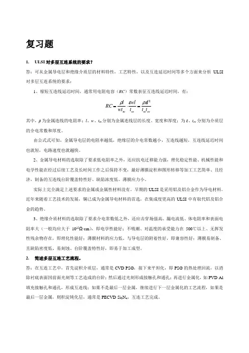
复习题1. ULSI 对多层互连系统的要求?答:可从金属导电层和绝缘介质层的材料特性,工艺特性,以及互连延迟时间等多个方面来分析ULSI 对多层互连系统的要求:1、缩短互连线延迟时间,通常用电阻电容(RC )常数表征互连线延迟时间,有:ox m ox m t t l t wl wt l RC 2ρεερ=⋅= 其中,ρ为金属连线的电阻率;l 、w 、t m 分别为金属连线层的长度、宽度和厚度;为ε、t ox 分别为介质层的介电常数和厚度。
由公式式可知,金属导电层的电阻率越低,绝缘层的介电常数越小,互连线越短,互连线延迟时间也就短,电路速度也就越快。
2、金属导电材料的选取除了要求低电阻率之外,还应抗电迁移能力强,理化稳定性能、机械性能和电学性能在经过后续工艺及长时间工作之后保持不变,最好薄膜淀积和图形转移等加工工艺简单、且经济,制备的互连线台阶覆盖特性好、缺陷浓度低、薄膜应力小。
实际上完全满足上述要求的金属或金属性材料没有。
早期的ULSI 是采用铝及铝合金作为导电材料。
近年来随着工艺技术的发展,铜已成为金属导电材料的首选,在集成度更高的ULSI 中有取代铝及铝合金的趋势。
3、绝缘介质材料的选取除了要求介电常数低之外,还应击穿场强高、漏电流低、体电阻率和表面电阻率大(一般均应大于1015Ω·cm ),即电学性能好;不吸潮、对温度的承受能力在500℃以上、无挥发性残余物存在,即理化性能好;薄膜材料的应力低、与导电层的附着性好,即兼容性好;薄膜易制备、且缺陷密度低、易刻蚀、台阶覆盖特性好,即易于加工成型。
2. 简述多层互连工艺流程。
答:在互连工艺中,首先淀积介质层,通常是CVD-PSG ;接下来平坦化,即PSG 的热处理回流,以消除衬底表面因前面光刻等工艺造成的台阶;然后通过光刻形成接触孔和通孔;再进行金属化,如PVD-Al 填充接触孔和通孔,形成互连线;如果不是最后一层金属,继续进行下一层金属化的工艺流程,如果是最后一层金属,则积淀钝化层,通常是PECVD-Si 3N 4,互连工艺完成。

1.集成电路的发展过程经历了哪些发展阶段?划分集成电路的标准是什么?集成电路的发展过程:•小规模集成电路(Small Scale IC,SSI)•中规模集成电路(Medium Scale IC,MSI)•大规模集成电路(Large Scale IC,LSI)•超大规模集成电路(Very Large Scale IC,VLSI)•特大规模集成电路(Ultra Large Scale IC,ULSI)•巨大规模集成电路(Gigantic Scale IC,GSI)划分集成电路规模的标准2.超大规模集成电路有哪些优点?1. 降低生产成本VLSI减少了体积和重量等,可靠性成万倍提高,功耗成万倍减少.2.提高工作速度VLSI内部连线很短,缩短了延迟时间.加工的技术越来越精细.电路工作速度的提高,主要是依靠减少尺寸获得.3. 降低功耗芯片内部电路尺寸小,连线短,分布电容小,驱动电路所需的功率下降.4. 简化逻辑电路芯片内部电路受干扰小,电路可简化.5.优越的可靠性采用VLSI后,元件数目和外部的接触点都大为减少,可靠性得到很大提高。
6.体积小重量轻7.缩短电子产品的设计和组装周期一片VLSI组件可以代替大量的元器件,组装工作极大的节省,生产线被压缩,加快了生产速度.3.简述双阱CMOS工艺制作CMOS反相器的工艺流程过程。
1、形成N阱2、形成P阱3、推阱4、形成场隔离区5、形成多晶硅栅6、形成硅化物7、形成N管源漏区8、形成P管源漏区9、形成接触孔10、形成第一层金属11、形成第一层金属12、形成穿通接触孔13、形成第二层金属14、合金15、形成钝化层16、测试、封装,完成集成电路的制造工艺4.在VLSI设计中,对互连线的要求和可能的互连线材料是什么?互连线的要求低电阻值:产生的电压降最小;信号传输延时最小(RC时间常数最小化)与器件之间的接触电阻低长期可靠工作可能的互连线材料金属(低电阻率),多晶硅(中等电阻率),高掺杂区的硅(注入或扩散)(中等电阻率)5.在进行版图设计时为什么要制定版图设计规则?—片集成电路上有成千上万个晶体管和电阻等元件以及大量的连线。
集成电路版图设计习题答案第2章 集成电路制造工艺【习题答案】1.硅片制备主要包括(直拉法)、(磁控直拉法)和(悬浮区熔法)等三种方法。
2.简述外延工艺的用途。
答:外延工艺的应用很多。
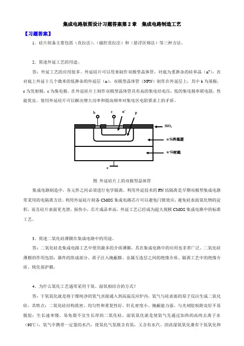
外延硅片可以用来制作双极型晶体管,衬底为重掺杂的硅单晶(n +),在衬底上外延十几个微米的低掺杂的外延层(n ),双极型晶体管(NPN )制作在外延层上,其中b 为基极,e 为发射极,c 为集电极。
在外延硅片上制作双极型晶体管具有高的集电结电压,低的集电极串联电阻,性能优良。
使用外延硅片可以解决增大功率和提高频率对集电区电阻要求上的矛盾。
图 外延硅片上的双极型晶体管集成电路制造中,各元件之间必须进行电学隔离。
利用外延技术的PN 结隔离是早期双极型集成电路常采用的电隔离方法。
利用外延硅片制备CMOS 集成电路芯片可以避免闩锁效应,避免硅表面氧化物的淀积,而且硅片表面更光滑,损伤小,芯片成品率高。
外延工艺已经成为超大规模CMOS 集成电路中的标准工艺。
3.简述二氧化硅薄膜在集成电路中的用途。
答:二氧化硅是集成电路工艺中使用最多的介质薄膜,其在集成电路中的应用也非常广泛。
二氧化硅薄膜的作用包括:器件的组成部分、离子注入掩蔽膜、金属互连层之间的绝缘介质、隔离工艺中的绝缘介质、钝化保护膜。
4.为什么氧化工艺通常采用干氧、湿氧相结合的方式?答:干氧氧化就是将干燥纯净的氧气直接通入到高温反应炉内,氧气与硅表面的原子反应生成二氧化硅。
其特点:二氧化硅结构致密、均匀性和重复性好、针孔密度小、掩蔽能力强、与光刻胶粘附良好不易脱胶;生长速率慢、易龟裂不宜生长厚的二氧化硅。
湿氧氧化就是使氧气先通过加热的高纯去离子水(95℃),氧气中携带一定量的水汽,使氧化气氛既含有氧,又含有水汽。
因此湿氧氧化兼有干氧氧化和en +SiO 2n -Si 外延层 n +Si 衬底水汽氧化的作用,氧化速率和二氧化硅质量介于二者之间。
实际热氧化工艺通常采用干、湿氧交替的方式进行。
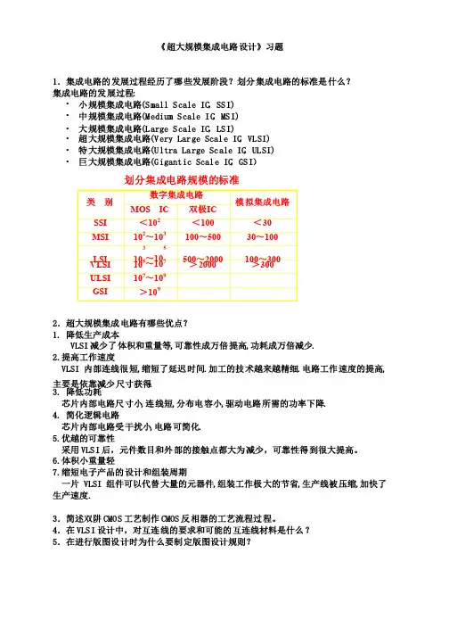
《超大规模集成电路设计》习题1.集成电路的发展过程经历了哪些发展阶段?划分集成电路的标准是什么?集成电路的发展过程:•小规模集成电路(Small Scale IC ,SSI)•中规模集成电路(Medium Scale IC ,MSI)•大规模集成电路(Large Scale IC ,LSI) •超大规模集成电路(Very Large Scale IC ,VLSI)•特大规模集成电路(Ultra Large Scale IC ,ULSI)•巨大规模集成电路(Gigantic Scale IC ,GSI )2.超大规模集成电路有哪些优点?1. 降低生产成本VLSI 减少了体积和重量等,可靠性成万倍提高,功耗成万倍减少.2.提高工作速度VLSI 内部连线很短,缩短了延迟时间.加工的技术越来越精细.电路工作速度的提高,主要是依靠减少尺寸获得. 3. 降低功耗芯片内部电路尺寸小,连线短,分布电容小,驱动电路所需的功率下降.4. 简化逻辑电路芯片内部电路受干扰小,电路可简化.5.优越的可靠性采用VLSI 后,元件数目和外部的接触点都大为减少,可靠性得到很大提高。
6.体积小重量轻7.缩短电子产品的设计和组装周期一片VLSI 组件可以代替大量的元器件,组装工作极大的节省,生产线被压缩,加快了生产速度.3.简述双阱CMOS 工艺制作CMOS 反相器的工艺流程过程。
4.在VLSI 设计中,对互连线的要求和可能的互连线材料是什么?5.在进行版图设计时为什么要制定版图设计规则?划分集成电路规模的标准数字集成电路类别MOS IC 双极IC 模拟集成电路SSI <102<100 <30 MSI 102~103100~500 30~100 LSI 103~105500~2000 100~300 VLSI 105~107>2000 >300 ULSI 107~109GSI >109在芯片尺寸尽可能小的前提下,使得即使存在工艺偏差也可以正确的制造出IC,尽可能地提高电路制备的成品率6.版图验证和检查主要包括哪些方面?u DRC(Design Rule Check):几何设计规则检查;对IC的版图做几何空间检查,保证能在特定的工艺条件下实现所设计的电路,并保证一定的成品率;u ERC(Electrical Rule Check):电学规则检查;检查电源(power)/地(ground)的短路,浮空的器件和浮空的连线等指定的电气特性;u LVS(Loyout versus Schematic):网表一致性检查;将版图提出的网表和原理图的网表进行比较,检查电路连接关系是否正确,MOS晶体管的长/宽尺寸是否匹配,电阻/电容值是否正确等;u LPE(Layout Parameter Extraction):版图寄生参数提取;从版图中提取晶体管的尺寸、结点的寄生电容、连线的寄生电阻等参数,并产生SPICE 格式的网表,用于后仿真验证;u POSTSIM:后仿真,检查版图寄生参数对设计的影响;提取实际版图参数、电阻、电容,生成带寄生量的器件级网表,进行开关级逻辑模拟或电路模拟,以验证设计出的电路功能的正确性和时序性能等,并产生测试向量。

复习题1.ULSI中对光刻技术的基本要求?答:一般来说,在ULSI中对光刻技术的基本要求包括五方面:①高分辨率。
随着集成电路集成度的不断提高,加工的线条越来越精细,要求光刻的图形具有高分辨率。
在集成电路工艺中,通常把线宽作为光刻水平的标志,一般也可以用加工图形线宽的能力来代表集成电路的工艺水平。
②高灵敏度的光刻胶。
光刻胶的灵敏度通常是指光刻胶的感光速度。
在集成电路工艺中为了提高产品的产量,希望曝光时间愈短愈好。
为了减小曝光所需的时间,需要使用高灵敏度的光刻胶。
光刻胶的灵敏度与光刻胶的成份以及光刻工艺条件都有关系,而且伴随着灵敏度的提高往往会使光刻胶的其它属性变差。
因此,在确保光刻胶各项属性均为优异的前提下,提高光刻胶的灵敏度已经成为了重要的研究课题。
③低缺陷。
在集成电路芯片的加工过程中,如果在器件上产生一个缺陷,即使缺陷的尺寸小于图形的线宽,也可能会使整个芯片失效。
通常芯片的制作过程需要经过几十步甚至上百步的工序,在整个工艺流程中一般需要经过10~20次左右的光刻,而每次光刻工艺中都有可能引入缺陷。
在光刻中引入缺陷所造成的影响比其他工艺更为严重。
由于缺陷直接关系到成品率,所以对缺陷的产生原因和对缺陷的控制就成为重要的研究课题。
④精密的套刻对准。
集成电路芯片的制造需要经过多次光刻,在各次曝光图形之间要相互套准。
ULSI中的图形线宽在1μm以下,因此对套刻的要求也就非常高。
一般器件结构允许的套刻精度为线宽的±10%左右。
这种要求单纯依靠高精度机械加工和人工手动操作已很难实现,通常要采用自动套刻对准技术。
⑤对大尺寸硅片的加工。
集成电路芯片的面积很小,即便对于ULSI的芯片尺寸也只有1~2cm2左右。
为了提高经济效益和硅片利用率,一般采用大尺寸的硅片,也就是在一个硅片上一次同时制作很多完全相同的芯片。
采用大尺寸的硅片带来了一系列的技术问题。
对于光刻而言,在大尺寸硅片上满足前述的要求难度更大。
而且环境温度的变化也会引起硅片的形变(膨胀或收缩),这对于光刻也是一个难题。
习题数电参考答案(终)第⼀章数字逻辑概论1.1 数字电路与数制信号1.1.1 试以表1.1.1所列的数字集成电路的分类为依据,指出下列IC器件属于何种集成度器件:(1)微处理器;(2)计数器;(3)加法器;(4)逻辑门;(5)4兆位存储器。
解:依照表1.1.1所⽰的分类,所列的五种器件:(1)、(5)属于⼤规模;(2)、(3)属于中规模;(4)属于⼩规模。
1.1.2⼀数字信号波形如图题1.1.2所⽰,试问该波形所代表的⼆进制数是什么?解:图题1.1.2所⽰的数字信号波形的左边为最⾼位(MSB),右边为最低位(LSB),低电平表⽰0,⾼电平表⽰1。
该波形所代表的⼆进制数为010110100。
1.1.3 试绘出下列⼆进制数的数字波形,设逻辑1的电压为5V,逻辑0的电压为0V。
(1)001100110011(2)0111010 (3)1111011101解:⽤低电平表⽰0,⾼电平表⽰1,左边为最⾼位,右边为最低位,题中所给的3个⼆进制数字的波形分别如图题1.1.3(a)、(b)、(c)所⽰,其中低电平为0V,⾼电平为5V。
1.1.4⼀周期性数字波形如图1.1.4所⽰,试计算:(1)周期;(2)频率;(3)占空⽐。
解:因为图题1.1.4所⽰为周期性数字波,所以两个相邻的上升沿之间持续的时间为周期,T=10ms。
频率为周期的倒数,f=1/T=1/0.01s=100Hz。
占空⽐为⾼电平脉冲宽度与周期的百分⽐,q=1ms/10ms×100%=10%。
1.2 数制1.2.1 ⼀数字波形如图1.2.1所⽰,时钟频率为4kHz,试确定:(1)它所表⽰的⼆进制数;(2)串⾏⽅式传送8位数据所需要的时间;(3)以8位并⾏⽅式传送的数据时需要的时间。
解:该波形所代表的⼆进制数为00101100。
时钟周期T=1/f=1/4kHz=0.25ms。
串⾏⽅式传送数据时,每个时钟周期传送1位数据,因此,传送8位数据所需要的时间t=0.25ms×8=2ms。

懂得1、Please illustrate the meaning of its voltage transfer characteristic to a logic gate, and describe the static behaviors showed in the voltage transfer characteristic curves.The electrical function of a gate is best expressed by its voltage transfer characteristic (VTC),which plots the output voltage as a function of the input voltage Vout=f(Vin).The high and low nominal voltage Voh and Vol;The gate or switching threshold voltage Vm,that is define as Vm=f(Vm)(The gate threshold voltage presents the midpoint of the switching characteristics,which is obtained when the output of a gate is short circuited to the input);The high and low input voltage Vih and Vil are defined by the point where the gain (=dVout/dVin)of the VTC equals -12、Please draw the voltage transfer characteristic curve of the inverter and label the static operation points in the VTC.3、Please describe the definition of noise margin and its physical significance(物理意义), then draw the figure of definition of noise margins.The noise margins represent the levels of noise that can be sustained(所允许的) when gates are cascaded. A measure of the sensitivity of a gate to noise is given by the noise margins NML(noise margin low) and NMH(noise margin high), which quantize the size of the legal “0” and “1”, respectively, and set a fixed maximum threshold on the noise value4、Please describe the meaning of the regenerative property and the conditions of a gate with regenerative property.A gate with regenerative property ensures that a disturbed signal converges back to a nominal voltage level after passing through a number of logical stages. The VTC should have a transient region (or undefined region) with a gain greater than 1 in absolute value, bordered by the two legal zones, where the gain should be less than 1 in absolute value5、What are the definitions of the fan-out and fan-in properties?The number that can be driven is termed the fan-out of circuit, that denotes the number of load gates N that are connected to the output of the driving gate. The fan-in of a gate is defined as the number of independent input nodes to the gate.6、How to describe the performance of a digital IC? Please illustrate the parameters used to characterize the transient performance of a logic family, and draw the associated figure of the definition of these parP ropagation delay time and rise/fall time can be used to characterize the transient performance of a logic family .Propagation delay time of a gate expresses the delay experienced by a signal when passing through a gate,which represent how quickly the gate responds to the changes at its inputs.Rise/fall time express how fast a signal transits between the different levels. Propagation delay time is defined as the period between the 50%transition points of the input and output signals.Rise/fall time is defined as the period between the 10% and 90% points of the total voltage transition at the output waveforms.1、Illustrate the basic structure and simple operation principle of MOS transistor.Four terminals:source, drain, gate, body; Vertical Structure: gate electrode, insulator, semiconductor substrate; Horizontal Structure: source region, channel region, drain region2、Illustrate the basic function of each terminal of MOS device, and describe the general terminal connections of NMOS and PMOS transistor, respectively.The source and the drain are the electrodes conducting the current. The gate electrode is thecontrolling terminal. The function of the body is secondaryIn NMOS devices, the source is defined as the n+ region which has a lower potential(电势) than the other n+ region, the drain. The source is the terminal with the higher potential in PMOS devices, The body is generally connected to a DC supply that is identical for all devices of the same type (GND for NMOS, VDD for PMOS).3、What does the transition (or input) characteristic of MOS transistor mean? And what conclusions we can find from the characteristic curve?It describes the relationship between the gate-source voltage and the drain-source current with the certain drain-source voltage .When the gate-source voltage is less than the threshold voltage, the conducting current is zero, that is, the NMOS transistor is in cutoff operation. When is larger than, the NMOS transistor is on.4、What does the current-voltage (or output) characteristic of MOS transistor mean? And what conclusions we can find from the I-V characteristic curve?.It describes the relationship between the drain-source voltage and the drain-source current with a certain gate-source voltageVgs > Vt , 0<VDS <VGS -VT : Linear modeThe inversion layer forms a continuous current path between the source and the drain.A drain current proportional to Vds will flow from the drain to the source through the conducting channel. The channel region acts as a voltage-controlled linear resister.5、Describe the operation modes of NMOS and PMOS transistors respectively, and define the corresponding ideal current equations.1、Explain the channel-length modulation, sub-threshold conduction, short-channel effect and narrow-channel effect. And illustrate their corresponding chief impacts on the device.This simple current equation prescribes a linear drain-bias dependence for the current in MOS transistors, determined by the empirical model parameter λ, called the channel-length modulation coefficientOne typical condition, which is due to the two-dimensional nature of channel current flow, is the sub-threshold conduction in small-geometry MOS transistors.As a working definition, a MOS transistor is called a short-channel device if its channel length is on the same order of magnitude as the depletion region thicknesses of the source and drain junctions.The short-channel effects that arise in this case are attributed to two physical phenomena: the limitations imposed on electron drift characteristics in the channel; the modification of the threshold voltage due to the shortening channel lengthMOS transistor that have channel widths on the same order of magnitude as the maxium depletion region thickness are defined as narrow channel devices.For MOSFET with small channel widths,the actual threshold voltage increases as a result of this extra depletion charge of the fringe depletion region.This fact is called narrow channel effect.2、Describe the three main components of the load capacitanceCL, when a logic gate is driving other fan-out gates. And sketch the capacitance model of NMOS transistor.Gate capacitances (of other inputs connected to out)Diffusion(or junction) capacitances (of drain/source regions)Routing capacitances (output to other inputs)1,Describe the basic structure and operation of a static CMOS inverter. Then draw theassociated transistor schematicThis structure consists of an enhancement-type NMOS transistor and an enhancement-type PMOS transistor, operating in complementary mode. So this configuration is called Complementary MOS (CMOS). The gate terminals of the PMOS and NMOS transistors are connected to form the inverter input. The drain terminals of the PMOS and NMOS transistors are connected to form the inverter output. The source and the substrate of the NMOS transistor are connected to the ground, while the source and body of PMOS transistor are connected to VDD The circuit topology is complementary push-pull in the sense that: For high input the NMOS transistor drives (pulls down) the output node while the PMOS transistor acts as the load, and for low input the PMOS transistor drives (pulls up) the output node while the NMOS transistor acts as the load.When the input is at VDD: The NMOS is on (conducting) while the PMOS is off (cut-off). A direct path exists between Vout and the ground node, resulting in a steady-state value of 0V at the output. When the input is at ground:The NMOS is off while the PMOS is on. A direct path exists between VDD and Vout, yielding a high output voltage (equal to VDD).Static CMOS logic:structure:The static CMOS style is really an extension of the static CMOS inverter to multiple inputs. A logic function in static CMOS must be implemented in both NMOS and PMOS transistors. It is the combination of the pull-up network(PUN) and the pull-down network(PDN). Each input always connects to PUN and PDN simultaneously. The function of the PUN is to provide a connection between the output and VDD anytime the output of the logic gate is meant to be 1 (based on the inputs). The function of the PDN is to connect the output to VSS when the output of the logic gate is meant to be 0.Opreation: The pull-down net should be “on” when the pull-up net is “off” and vice versa. For any given input combination, the output is connected either to VDD or to ground via a low-resistance path. A DC current path between the VDD and ground is not established for any of the input combinations. With the complementary nature of NMOS and PMOS, the pull-up or the pull-down is “on” alternately to implement the logic operation.Discuss the main problems for high fan-in static CMOS gates and the associated techniques for fast complex gates.tpHL = 0.69 Reqn(C1+2C2+3C3+4CL); Propagation delay deteriorates(恶化) rapidly as a function of fan-in quadratically in the worst case, Gates with a fan-in greater than 4 become excessively slow and must be avoided.tPLH increases linearly due to the linearly increasing value of the diffusion capacitance;tPHL increase quadratically due to the simultaneous increase the resistance and internal capacitance in serial part.Transistor sizing: as long as fan-out capacitance dominatesProgressive transistor sizing: This approach reduces the dominant resistance, while keeping the increase in capacitance within boundsTransfer gate:Configuration:The source and drain nodes serve as inputs and outputs, while the gate node serves as the control input, the body node is connected to the power/ground Operation: For NMOS transfer gate,it turns on while the gate control terminal goes high, and the input signal will be delivered to the output node; it turns off while the gate control terminal goes low, and the output node will be impedance.CMOS transmission gate:Configuration: The CMOS transmission gate consists of one NMOS and one PMOS transistor, with the source and drain connected in parallel; The gate voltages appliedto these two transistors are also set to be complementary signals. The substrate terminal of the NMOS transistor is connected to ground and the substrate terminal of the PMOS transistor is connected to Vdd.Operation: If the control signal C is logic-high (equal to Vdd), then both transistors are turned on and provide a low-resistance current path between the input and output nodes. If the control signal C is logic-low, then both transistors will be off, and the path between the input and output nodes will be in the high-impedance state. The weakness of one device is overcome by the strength of the other device, whether the output is transmitting a high or low value. This is a clear advantage of the CMOS transfer gate over the single transistor counterpart.DCVLS:Operation: Assume now that, for a given set of inputs, PDN1 conducts while PDN2 does not, and that Out and out are initially high and low, respectively. Turning on PDN1: Causes Out to be pulled down (below VDD−|VTP |); Out is in a high impedance state, as M2 and PDN2 are both turned off. At the point M2 turns on and starts charging out非to VDD — eventually turning off M1; This in turn enables Out to discharge all the way to GND.XOR/XNOR: When the signals A and B have the same values, there is one conducting path either AB or A非B非; Then the output F is pulled down;At the same time, the other pull-down paths connected to the F非are both turned off. When F is pulled down below VDD−|VTP |, M2 t urns on and starts charging F非to VDD —eventually turning off M1 and pulling down F to Gnd. When the signals A and B have the different values, there is one conducting path either AB非or A非B; Then the output F非is pulled down; At the same time, the other pull-down paths connected to the F are both turned off. When F非is pulled down below VDD−|VTP |, M1 turns on and starts charging F to VDD —eventually turning off M2 and pulling down F非to Gnd.Precharge-Evaluate dynamic CMOS:Operation: Precharge (when the clock signal Φ= 0):The PMOS precharge transistor MP is conducting while the complementary NMOS transistor MN is off. The output load capacitance is precharged to VDD by MP, then VOH=VDD;The input voltages have no influence yet upon the output level since the complementary NMOS transistor MN is off. Evaluate (when the clock signal Φ=1):The precharge transistor MP turns off while the NMOS evaluate transistor MN turns on. The output node voltage may now remain at the logic-high level or drop to a logic low, depending on the input voltage levels: If the input signals create a conducting path between the output node and the ground, PDN is on, and the output capacitance will discharge toward VOL=0;Otherwise, when PDN is off, the output voltage remains at VOH= VDD.Domino dynamic CMOS logic:When Φ=0, during precharge: The output of the n-type dynamic gate is charged up to VDD, and the output of the inverter is set to 0. When Φ=1, during evaluation: The dynamic gate conditionally discharges, and there are two possibilities: The output node of the dynamic CMOS stage is either discharged to a low level through the NMOS circuitry (1 to 0 transition), or it remains high. Consequently, the inverter output voltage can also make at most one transition during the evaluation phase, from 0 to 1.TSPC dynamic CMOS logic:Configuration:If one constrains a NORA stage to have only n-precharge gates, and not static gates, then a p-channel transistor can be eliminated from the clocked latch; The dynamic circuit technique to be presented in that it uses only one-phase clock signal, so no clock skew problem exists. The NORA design style can be simplified so that a single clock is sufficient. For the doubled n-C2MOS latch, when φ= 1, the latch is in the transparent evaluate mode and corresponds to 2 cascaded inverters (non-inverting); For the doubled n-C2MOS latch, when φ= 0, both inverters are disabled (hold mode) -- only the pull-up network is still active.Pipelined NORA dynamic CMOS system:Configuration: Consists of an np-CMOS logic sequence and a clocked CMOS output buffer; A pipelined system can be constructed by simply cascading alternating φ-section and φ -section, meaning that evaluation occurs during active φ and φ respectively;Operation:φ=0, during hold mode :N block performs the precharge operation and pulls node Out1 up to VDD through the p-type device Mp1, while p block performs the discharge operation and pulls the node Out2 down to zero through the n-type device Mn2; The clocked CMOS latch will not be in operation and the previous output voltage will be stored on the output load capacitor CL. φ=1, during evaluate mode:All cascaded NMOS and PMOS blocks evaluate output levels one after the other, and then the signal Out2 will be inversed to the output node by the clocked CMOS latch in operation;Operation Mode: Evaluate―Hold: All logic stages perform the precharge-discharge operation when the clock is high, and all stages evaluate output levels when the clock is low. Therefore, wewill call this circuit a section, meaning that evaluation occurs during active .Clocked CMOS dynamic circuit:Basic Structure:A pair of PMOS and NMOS transistors controlled by the complementary clock signals are cascaded in the pullup and pulldown paths of the static CMOS gate, respectively, then a CMOS logic gate can be synchronized with a clock. Operation: φ=1, during evaluation mode:The transistors Mp1 and Mp2 are both turned on, then this gate can evaluate normally as a CMOS inverter to generate the logic output In非; φ=0 , during hold mode: Both transistors Mp1 and Mp2 are off, decoupling the output from the input. The CMOS circuit cannot conduct and evaluate, then the output Q retains its previous value stored on the output capacitor CL.Sequential logic:Virtually all useful systems require storage of state information, leading to another class of circuits called sequential logic circuits. In these circuits, the output not only depends upon the current values of the inputs, but also upon preceding output values. In other words, a sequential circuit remembers some of the past history of the system; A sequential circuit consists of a combinational circuit and a memory block in the feedback loop.Combination logic:In all logic circuits described so far, the output is directly related to the input. Typically, there are no feedback loops between the output and the input in these circuits (also classified as non-regenerative circuits), so the outputs are always a logical combination of the inputs. As a class, these circuits are known as combinational logic circuits. Combinational logic circuits, described earlier, have the property that the output of a logic block is only a function of the current input values, assuming that enough time has elapsed for the logic gates to settle. Static storage:preserve state as long as the power is on;are built using positive feedback or regeneration with an intentional connection between the output and the input;useful when updates are infrequent (clock gating)Dynamic storage:store state on parasitic capacitors;only hold state for short periods of time (milliseconds);require periodic refresh to annihilate charge leakage;usually simpler, so higher speed and lower power;useful in datapath circuits that require high performance levels and are periodically clockedLatch: level sensitive circuit that passes inputs to Q when the clock is high (or low);input sampledon the falling edge of the clock is held stable when clock is low (or high)Register or Flip-flops (edge-triggered): edge sensitive circuits that only sample the inputs on a clock transitionpositive edge-triggered: 0- 1negative edge-triggered: 1 -0built using latches (e.g., master-slave flip-flops)。
《数字集成电路基础》作业答案第一次作业1、查询典型的TTL与CMOS系列标准电路各自的VIH、VIL、VOH和VOL,注明资料出处。
2、简述摩尔定律的内涵,如何引领国际半导体工艺的发展。
第二次作业1、说明CMOS电路的Latch Up效应;请画出示意图并简要说明其产生原因;并简述消除“Latch-up”效应的方法。
答:在单阱工艺的MOS器件中(P阱为例),由于NMOS管源与衬底组成PN结,而PMOS 管的源与衬底也构成一个PN结,两个PN结串联组成PNPN结构,即两个寄生三极管(NPN 和PNP),一旦有因素使得寄生三极管有一个微弱导通,两者的正反馈使得电流积聚增加,产生自锁现象。
影响:产生自锁后,如果电源能提供足够大的电流,则由于电流过大,电路将被烧毁。
消除“Latch-up”效应的方法:版图设计时:为减小寄生电阻Rs和Rw,版图设计时采用双阱工艺、多增加电源和地接触孔数目,加粗电源线和地线,对接触进行合理规划布局,减小有害的电位梯度;工艺设计时:降低寄生三极管的电流放大倍数:以N阱CMOS为例,为降低两晶体管的放大倍数,有效提高抗自锁的能力,注意扩散浓度的控制。
为减小寄生PNP管的寄生电阻Rs,可在高浓度硅上外延低浓度硅作为衬底,抑制自锁效应。
工艺上采用深阱扩散增加基区宽度可以有效降低寄生NPN管的放大倍数;具体应用时:使用时尽量避免各种串扰的引入,注意输出电流不易过大。
2、什么是器件的亚阈值特性,对器件有什么影响?答:器件的亚阈值特性是指在分析MOSFET时,当Vgs<Vth时MOS器件仍然有一个弱的反型层存在,漏源电流Id并非是无限小,而是与Vgs呈现指数关系,这种效应称作亚阈值效应。
影响:亚阈值导电会导致较大的功率损耗,在大型电路中,如内存中,其信息能量损耗可能使存储信息改变,使电路不能正常工作。
3、什么叫做亚阈值导电效应?并简单画出logI D-V GS特性曲线。
答:GS在分析MOSFET时,我们一直假设:当V GS下降到低于V TH时器件会突然关断。
电路性能:PROBLEM 1. Consider an isolated 2mm long and 1μm wide M1(Metal1)wire over a silicon substrate driven by an inverter that has zero resistance and parasitic output capccitance. How will the wire delay change for the following cases? Explain your reasoning in each case.a. If the wire width is doubled.b. If the wire length is halved.c. If the wire thickness is doubled.d. If thickness of the oxide between the M1 and the substrate is doubled. PROBLEM 2. A two-stage buffer is used to drive a metal wire of 1 cm. The first inverter is of minimum size with an input capacitance C i=10 fF and an internalpropagation delay t p0=50 ps and load dependent delay of 5ps/fF. The width of the metal wire is 3.6 μm. The sheet resistance of the metal is 0.08 Ω, the capacitance value is 0.03 fF/μm2 and the fringing field capacitance is0.04fF/μm.a. What is the propagation delay of the metal wire?b. Compute the optimal size of the second inverter. What is the minimum delay through the buffer?PROBLEM 3. An NMOS transistor is used to charge a large capacitor, as shown the following Figure. The minimum size device, (0.25/0.25) for NMOS and (0.75/0.25) for PMOS, has the on resistance 35 kΩ.a. Determine the t pLH of this circuit, assuming an ideal step from 0 to 2.5V at the input node.b. Assume that a resistor R S of 5 kΩ is used to discharge the capacitance toground. Determine t pHL.c. The NMOS transistor is replaced by a PMOS device, sized so that k p is equal to the k n of the original NMOS. Will the resulting structure be faster? Explain why or why not.PROBLEM 4.The figure below assembles a RTL circuit where the active device is a NMOS transistor which has a resistive load. Assume the switch model behavior of the NMOS transistor. When V in <1.25V, the resistance of the transistor is infinite. When V in ≥1.25V, the transistor can be modeled as having a resistance of 150 ohms.A. Determine the values for V OH and V OL . Explain your answer.B. Calculate t pLH and t pHL to obtain the average propagation delay, t p .Solution:Vin 50fFPROBLEM 5. The next figure shows two implementations of MOS inverters. The first inverter uses only NMOS transistors.a. Calculate V OH, V OL, V th for each case.b. Find V IH, V IL, N ML and N MH for each inverter and comment on the results. How can you increase the noise margins and reduce the undefined region? 0.25um CMOS工艺(L=Lmin) MOS管参数Problem 6: We want to design a minimum sized CMOS inverter with 0.25um process( =0.12um). The minimum sized NMOS transistor ’s layers are listed and shown below in Figure below.A. Determine and list the following:a. Minimum Transistor Lengthb. Minimum Transistor Widthc. Minimum Source/Drain Aread. Minimum Source/Drain PerimeterPlease list the design rules you come across that lead to your results.B. We desire the minimum sized CMOS inverter with a symmetrical VTC (V Th =V DD /2) in the 0.25um technology. Calculate the following for the pull-up PMOS transistor in the design.a. Minimum Transistor Lengthb. Minimum Transistor Widthc. Minimum Source/Drain Aread. Minimum Source/Drain PerimeterAssume the following:V DD = 2.5V, and refer to the tables in the below.C. Using the same minimum size inverter from part B, determine the input capacitance (i.e. the load it presents when driven) and the total load capacitance that the inverter presents.D. Calculate t pLH and t pHL to obtain the average propagation delay, t p .Rules are:i) Poly minimum width = 0.24umii) Minimum active width = 0.36umiii) Minimum contact size = 0.24um*0.24umiv) Minimum spacing from contact to gate = 0.24umv) Active enclosure of contact = 0.12umAnswer:A:a. L = 0.24umb. W = 0.48umc. L drain = 0.24um+0.24um+0.12um = 0.6umA D =A S = 0.48 * 0.6um = 0.288 um 2d. P D =P S =0.6um*2+0.48um = 1.68umB:2n T0,Th Th p T0,DD p n R R R p T0,DD n T0,Th V V V V V k k 得出k k 11k 1)V (V V V ⎪⎪⎭⎫ ⎝⎛--+==+⋅++=查表得出一下参数:V T0p = -0.43V V T0n = 0.4V K n ’=115×10-6 A/V 2 K p ’=30×10-6A/V 2 另:L=0.24um, W n =0.48um带入上述公式计算得出:K R =0.965 W p =1.907umWe assume u n =2.5u p and can calculatea. Lp=0.24µmb. W p = 1.907 µmc. A D = 1.907µm *0.6µm =1.1442 µm 2d. P D = 2*0.6µm +1.2µm =3.107 µmC:NMOS:C gn = C ox L n W n = 0.6912 fFNMOS 管衬底接0V ,输出从1→0(V 1=-2.5V 变为V 2=-1.25V):()()()[]()()()[]0.615264fFC C C fF0.2869940.61281.68K C P C 0.44m 0.61V φV φm)(1V V φK fF 32832057022880K C A C 0.5m 0.57V φV φm)(1V V φK dbsw db dbn1eqsw j D dbsw m 11bsw m 12bsw 12m bsw eq eq j D db m 11b m 12b 12m b eq =+==⨯⨯====---⋅----==⨯⨯====---⋅----=----.0侧壁:...底部:输出从0→1(V 1=0V 变为V 2=-1.25V):()()()[]()()()[]fF0.836064C C C fF0.3810240.81281.68K C P C 0.44m 0.81V φV φm)(1V V φK fF 0.455040.7920.288K C A C 0.5m 0.79V φV φm)(1V V φK dbsw db dbn2eqsw j D dbsw m 11bsw m 12bsw 12m bsw eq eq j D db m 11b m 12b 12m b eq =+==⨯⨯====---⋅----==⨯⨯====---⋅----=----.0侧壁:底部:PMOS:C gp = C ox L p W p ) =2.74608 fFPMOS 管衬底接2.5V ,输出从1→0(V 1= 0V 变为V 2=-1.25V):()()()[]()()()[]fF2C C C fF0.58784440.8622K C P C 0.32m 0.86V φV φm)(1V V φK fF 10.7911K C A C 0.48m 0.79V φV φm)(1V V φK dbsw db dbp1eqsw j D dbsw m 11bsw m 12bsw 12m bsw eqsw eq j D db m 11b m 12b 12m b eq 3052886..0109.3侧壁:7174442.9.1442.=+==⨯⨯====---⋅----==⨯⨯====---⋅----=----底部:输出从0→1(V 1=-1.25V 变为V 2= -2.5V):()()()[]()()()[]fF1.7614342C C C fF0.4787860.70.223K C P C 0.32m 0.7V φV φm)(1V V φK fF 10.591.91K C A C 0.48m 0.59V φV φm)(1V V φK dbsw db dbp2eqsw j D dbsw m 11bsw m 12bsw 12m bsw eqsw eq j D db m 11b m 12b 12m b eq =+==⨯⨯====---⋅----==⨯⨯====---⋅----=----109.侧壁:2826482.1442.底部:如果m 以0.5计算:NMOS 管衬底接0V ,输出从1→0(V 1=-2.5V 变为V 2=-1.25V):()()()[]0.596448fFC C C fF0.268120.57281.68K C P C fF 32832057022880K C A C 0.57V φV φm)(1V V φK K dbsw db dbn1eqsw j D dbsw eq j D db m 11b m 12b 12m b eqsw eq =+==⨯⨯===⨯⨯===---⋅----==--.0...底部: 输出从0→1(V 1=0V 变为V 2=-1.25V):()()()[]fF0.826656C C C fF0.3716160.79281.68K C P C fF0.455040.7920.288K C A C 0.79V φV φm)(1V V φK K dbsw db dbn2eqsw j D dbsw eq j D db m 11b m 12b 12m b eqsw eq =+==⨯⨯===⨯⨯===---⋅----==--.0底部:PMOS 管衬底接2.5V ,输出从1→0(V 1= 0V 变为V 2=-1.25V):()()()[]fF 2C C C fF0.54034420.7922K C P C fF1.71744420.79911K C A C 0.79V φV φm)(1V V φK K dbsw db dbp1eqsw j D dbsw eq j D db m 11b m 12b 12m b eqsw eq 2577884..0109.3.1442.=+==⨯⨯===⨯⨯===---⋅----==--底部:输出从0→1(V 1=-1.25V 变为V 2= -2.5V):()()()[]fF 1.6290372C C C fF0.38986860.570.22K C P C fF10.571.91K C A C 0.57V φV φm)(1V V φK K dbsw db dbp2eqsw j D dbsw eq j D db m 11b m 12b 12m b eqsw eq =+==⨯⨯===⨯⨯===---⋅----==--109.32391686.1442.底部:D :C load 计算:C load =C wire +C g +C gd,n +C gd,p +C db,n +C db,p≈C g +C db,n +C db,pC g = C gn + C gp =0.6912+2.74608=3.43728 fF输出从1→0(V 1= 0V 变为V 2=-1.25V):C load≈C g +C db,n +C db,p =6.3578326 fF16.32ps1V )V 4(V ln V V 2V )V (V k C A/V 10230k L W k DD T0n DD T0n DD T0n T0n DD n load PHL 26'n nn n =⎥⎦⎤⎢⎣⎡⎪⎪⎭⎫ ⎝⎛--+--=⨯=⨯=-τ 输出从0→1(V 1=-1.25V 变为V 2= -2.5V):C load≈C g +C db,n +C db,p =6.0347782 fF15.33ps 1V )V 4(V ln V V V 2)V (V k C A/V 10238.375k L W k DD T0p DD T0pDD T0p T0pDD p load PLH 26'p p p p =⎥⎥⎦⎤⎪⎪⎭⎫ ⎝⎛--+⎢⎢⎣⎡--=⨯=⨯=-τ如果以m=0.5,则:输出从1→0(V 1= 0V 变为V 2=-1.25V):C load≈C g +C db,n +C db,p =6.2915162 fF16.147ps1V )V 4(V ln V V 2V )V (V k C DD T0n DD T0n DD T0n T0n DD n load PHL =⎥⎦⎤⎢⎣⎡⎪⎪⎭⎫ ⎝⎛--+--=τ 输出从0→1(V 1=-1.25V 变为V 2= -2.5V):C load≈C g +C db,n +C db,p =5.8929732 fFps 1V )V 4(V ln V V V 2)V (V k C DD T0p DD T0p DD T0p T0pDD p load PLH 97.14=⎥⎥⎦⎤⎪⎪⎭⎫ ⎝⎛--+⎢⎢⎣⎡--=τ PROBLEM 7.We want to design a minimum sized CMOS inverter with 0.25um process(λ=0.12um) and desire the inverter with a symmetrical VTC (V Th =V DD /2) . The minimum sized NMOS transistor’s layers are shown as problem 6. Assume the following:V DD = 2.5V, and refer to the tables in the below.A. Determine the input capacitance (i.e. the load it presents when driven) and the total load capacitance that the inverter presents.B. Calculate t pLH and t pHL to obtain the average propagation delay, t p .PROBLEM 8. Sizing a chain of inverters.a. In order to drive a large capacitance (CL = 20 pF) from a minimum size gate (with input capacitance Ci = 10fF), you decide to introduce a two-staged buffer as shown in the following figure. Assume that the propagation delay of a minimum size inverter is 70 ps. Also assumethat the input capacitance of a gate is proportional to its size. Determine the sizing of the two additional buffer stages that will minimize the propagation delay.b. If you could add any number of stages to achieve the minimum delay, how many stages would you insert?What is the propagation delay in this case?c. Describe the advantages and disadvantages of the methods shown in (a) and (b).PROBLEM 9. Consider a CMOS inverter with the following parameters:V T0,n=1.0V V T0,p=-1.2V μn C ox=45uA/V2μp C ox=25uA/V2 (W/L)n=10 (W/L)p=20The power supply voltage is 5V, and the output load capacitance is 1.5pF.a. Calculate the rise time and the fall time of the output signal using average current method.b. Determine the maximum frequency of a periodic square-wave input signal so that the output voltage can still exhibit a full logic swing from 0V to 5V in each cycle.c. Calculate the dynamic power dissipation at this frequency.d. Assume that the output load capacitance is mainly dominated by fixedfan-out component( which are independent of W n and W p). We want tore-design the inverter so that the propagation delay times are reduced by 25%. Determine the required channel dimensions of the nMOS and the pMOS transistors. How does this re-design influence the switching (inversion) threshold?PROBLEM 10. Consider the following low swing driver consisting of NMOS devi ces M1 and M2. Assume that the inputs IN and IN’ have a 0V to 2.5V swing and that V IN = 0V when V IN’ = 2.5V and vice-versa. Also assume thatthere is no skew between IN and IN’ (i.e., the inverter delay to derive IN from IN is zero).a. What voltage is the bulk terminal of M2 connected to?b. What is the voltage swing on the output node as the inputs swing from 0V to2.5V. Show the low value and the high value.c. Assume that the inputs IN and IN have zero rise and fall times. Assume a zero skew between IN and IN’. Determine the low to high propagation delay for charging the output node measured from the the 50% point of the input to the 50% point of the output. Assume that the total load capacitance is 1pF, including the transistor parasitics.MOS管参数参照题4。
1Chapter 11 Problem SetChapter 11PROBLEMS1.[E, None, 11.6] For this problem you are given a cell library consisting of full adders and two-input Boolean logic gates (i.e. AND, OR, INVERT, etc.).a.Design an N-bit two's complement subtracter using a minimal number of Boolean logicgates. The result of this process should be a diagram in the spirit of Figure 11.5 . Specifythe value of any required additional signals (e.g., C in ).b.Express the delay of your design as a function of N , tcarry , t sum , and the Boolean gate delays(t and , t or , t inv , etc.).2.[M, None, 11.6] A magnitude comparator for unsigned numbers can be constructed using fulladders and Boolean logic gates as building blocks. For this problem you are given a celllibrary consisting of full adders and arbitrary fan-in logic gates (i.e., AND, OR, INVERTER,etc.).a.Design an N -bit magnitude comparator with outputs and A = B using a minimalnumber of Boolean logic gates. The result of this process should be a diagram in the spiritof Figure 11.5. Specify the value of any required control signals (e.g., C in ).b.Express the delay of your design in computing the two outputs as a function of N , tcarry ,t sum , and the Boolean gate delays (t and , t or , t inv , etc.).3.3.[E, None, 11.6] Show how the arithmetic module in Figure 0.1 can be used as a comparator.Derive an expression for its propagation delay as a function of the number of bits.4.[E, None, 11.6] The circuit of Figure 11.2 implements a 1-bit datapath function in dynamic(precharge/evaluate) logic.a.Write down the Boolean expressions for outputs F and G . On which clock phases are out-puts F and G valid?b.To what datapath function could this unit be most directly applied (e.g., addition, subtrac-tion, comparison, shifting)?5.[M, None, 11.3] Consider the dynamic logic circuit of Figure 0.2 .a.What is the purpose of transistor M1? Is there another way to achieve the same effect, butwith reducing capacitive loading on the clock Φ?A B ≥Figure 0.1Arithmetic module.a i a ib j b jc jd jc j +1j+1c 0c 1d 0d 1c 1c 2d 1d 2c 2c 3d 2d 3c 3c 4d 3d 4a 0b 0a 1b 1a 2b 2a 3b 32Chapter 11 Problem Setb.How can the evaluation phase of F be sped up by rearranging transistors? No transistorsshould be added, deleted, or resized.c.Can the evaluation of G be sped up in the same manner? Why or why not?6.[M, SPICE, 11.3] The adder circuit of Figure 0.3 makes extensive use of the transmissiongate XOR. V DD = 2.5 V.a.Explain how this gate operates. Derive the logic expression for the various circuit nodes.Why is this a good adder circuit?b.Derive a first-order approximation of the capacitance on the C o -node in equivalent gate-capacitances. Assume that gate and diffusion capacitances are approximately identical.Compare your result with the circuit of Figure 11-6 .c.Assume that all transistors with the exception of those on the carry path are minimum-size. Use 4/0.25 NMOS and 8/0.25 PMOS devices on the carry-path. Using SPICE simu-lation, derive a value for all important delays (input-to-carry, carry-to-carry, carry-to-sum).A C inB B A ΦΦA B C in ABC inF GFigure 0.2Datapath module bit-slice.M 1Figure 0.3Quasi-clocked adder circuit.A A iV C oC i Signal setup Carry generationSum generationDigital Integrated Circuits - 2nd Ed 37.[M, None, 11.3] The dynamic implementation of the 4-bit carry-lookahead circuitry from Fig.11-21 can significantly reduce the required transistor count.a.Design a domino-logic implementation of Eq. 11.17 . Compare the transistor counts of thetwo implementations.b.What is the worst-case propagation delay path through this new circuit?c.Are there any charge-sharing problems associated with your design? If so, modify yourdesign to alleviate these effects.8.[C, None, 11.3] Figure 0.4 shows a popular adder structure called the conditional-sum adder.Figure 0.4.a shows a four-bit instance of the adder, while 0.4.b gives the schematics of thebasic adder cell. Notice that only pass-transistors are used in this implementation.a.Derive Boolean descriptions for the four outputs of the one-bit conditional adder cell.b.Based on the results of describe how the schematic of 0.4.a results in an addition.c.Derive an expression for the propagation delay of the adder as a function of the number ofbits N . You may assume that a switch has a constant resistance R on when active and thateach switch is identical in size.9.[M, None, 11.3] Consider replacing all of the NMOS evaluate transistors in a dynamicManchester carry chain with a single common pull-down as shown in Fgure 0.5.a. Assumethat each NMOS transistor has (W /L )N = 0.5/0.25 and each PMOS has (W /L )P = 0.75/0.25.Further assume that parasitic capacitances can be modeled by a 10 fF capacitor on each of theFigure 0.4Conditional-sum adder.A A B B A A B S 0A A B B AA B S 1AB A A AC 0ABA AAC 1(b) Conditional adder cell (a) Four-bit conditional-sum adderS 0S 1S 2S 3C out Conditional Cell Conditional Cell Conditional Cell ConditionalCellC 1C 0S 1S 0C 1C 0S 1S 0C 1C 0S 1S 0C 1C 0S 1S 0B 3A 3B 2A 2B 1A 1B 0A 04Chapter 11 Problem Setinternal nodes: A , B , C , D , E , and F . Assume all transistors can be modeled as linear resistorswith an on-resistance, R on = 5 k Ω.a.Does this variation perform the same function as the original Manchester carry chain?Explain why or why not.b.Assuming that all inputs are allowed only a single zero-to-one transition during evalua-tion, will this design involve charge-sharing difficulties? Justify your answer.plete the waveforms in Figure 0.5b for P 0 = P 1 = P 2 = P 3 = 2.5 V and G 0 = G 1 = G 2 =G 3 = 0 V. Compute and indicate t pHL values for nodes A , E , and F . Compute and indicate10.[M, None, 11.3] Consider the two implementations of Manchester carry gates in Figure 11-8.pare the delay per segment of the two implementationsb.Compare the layout complexities of the two gates using stick diagrams.c.In the precharged Manchester carry chain using the gate from b. find the probability thatthe carry signal is propagated from the 15th to the 16thbit of a 32-bit adder, assuming ran-dom inputs.11.[C, None, 11.3] Consider the Radix-4 and Radix-2 Kogge-Stone adders from Figures 11-22and 11-27 extended to 64-bits. All gates are implemented in domino and all gates in a stagehave the same size. The adders have an overall fanout (electrical effort) of 6.ing logical effort, identify the critical path.b.Size the gates for minimum delay (hint: don't forget to factor in branching). Which adderis faster?c.Let's now consider sparse versions of each of the above trees. In a tree with a sparseness of2, only every other carry is computed and it is used to select 2 sums. Similarly, a tree witha sparseness of 4 computes every fourth carry - and that carry signal is used to select 4sums. Repeat a. and b. for Radix-2 and Radix-4 trees with sparseness of 2 and 4 and com-pare their speed. Which adder is fastest?pare the switching power of all adders analyzed in this problem.12.[C, None, 11.3] In this problem we will analyze a carry-lookahead adder proposed by H. Lingmore than 20 years ago, but still among the fastest adders available. In a conventional adder,in order to add two numbersA = a n −12n −1 + a n −22n −2 + .... + a 020B = b n −12n −1 + b n −22n −2 + .... + b 020we first compute the local carry generate and propagate terms:P 0C in P 1G 0P 2G 1P 3G 2G 3φφV DD Figure 0.5Alternative dynamic Manchester carry-chain adder.A B C D E F (a) Circuit schematic (b) Partial waveformsφAEFCDigital Integrated Circuits - 2nd Ed 5g i = a i b i pi = a i + b ithen, with a ripple or a tree circuit we form the global carry-out terms resulting from the recurrence relation:G i = g i + p i G i −1Finally, we form the sum of A and B using local expressions:In the conventional adder, the terms G i have, as described, a physical significance. However,an arbitrary function could be propagated, as long as sum terms could be derived. Ling'sapproach is to replace G i with:H i = G i + Gi −1i.e. H i is true if "something happens at bit i " - there is a carry out or a carry in. H i is so-called"Ling's pseudo-carry".a.Show that:H i = g i + ti −1H i −1where p i = a i + b i (it was Ling’s idea to change the notation).b.Find a formula for computing the sum out of the operands and Ling's pseudo-carry.c.Unroll the recursions for G i and H i for i = 3. You should get the expressions fpr G 3 and H 3as a function of the bits of input operands. Simplify the expressions as much as possible.d.Implement the two functions using n-type dynamic gates. Draw the two gates and size thetransistors. Which one helps us build a faster adder? Explain your answer.13.[M, None, 11.4] An array multiplier consists of rows of adders, each producing partial sumsthat are subsequently fed to the next adder row. In this problem, we consider the effects ofpipelining such a multiplier by inserting registers between the adder rows.a.Redraw Figure 11-31 by inserting word-level pipeline registers as required to achievemaximal benefit to throughput for the 4x 4 multiplier. Hint: you must use additional regis-ters to keep the input bits synchronized to the appropriate partial sums.b.Repeat for a carry-save, as opposed to ripple-carry, architecture.c.For each of the two multiplier architectures, compare the critical path, throughput, andlatency of the pipelined and nonpipelined versions.d.Which architecture is better suited to pipelining, and how does the choice of a vector-merging adder affect this decision?14.[M, None, 11.4] Estimate the delay of a 16x16 Wallace tree multiplier with the final adderimplemented using a Radix-4 tree. One FA has a delay of t p , a HA 2/3*t p and a CLA stage½*t p .15.[E, None, 11.5] The layout of shifters is dominated by the number of wires running through acell. For both the barrel shifter and the logarithmic shifter, estimate the width of a shifter cellas a function of the maximum shift-width M and the metal pitch p .16.[E, None, 11.7] Consider the circuit from Figure 0.7 . Modules A and B have a delay of 10 nsand 32 ns at 2.5V, and switch 15 pF and 56 pF respectively. The register has a delay of 2 nsand switches 0.1 pF. Adding a pipeline register allows for reduction of the supply voltagewhile maintaining throughput. How much power can be saved this way? Delay with respectto V DD can be approximated from Figure 11-57.17.[E, None, 11.7] Repeat Problem 16, using parallelism instead of pipelining. Assume that a 2-to-1 multiplexer has a delay of 4 ns at 2.5 V and switches 0.3 pF. Try parallelism levels of 2and by 4. Which one is preferred?S i p i G i 1–⊕=6Chapter 11 Problem Set DESIGN PROBLEMUsing the 0.25 µm CMOS technology, design a static 32-bit adder, with the fol-lowing constraints:1.input capacitance on each bit is limited to not more than 50fF.2.each bit is loaded with 100fF.Use a carry lookahead tree of your choice for implementation. The goal is toachieve the shortest propagation delay.Determine the logic design of the adder and W and L of all transistors.Initially size the design using the method of logical effort. Estimate the capaci-tance of carry signal wires based on the floorplan. Verify and optimize thedesign using SPICE. Compute also the energy consumed per transition. If youhave a layout editor available, perform the physical design, extract the real cir-cuit parameters, and compare the simulated results with the ones obtained ear-lier. For implementation use the 144λ.bit-slice pitch, that corresponds to 36metal-1 tracks. Use metal 1 for cell-level power distrbution and intra-cell rout-ing, metal-2 for short interconnect and metal-3 and metal-4 for long carries.R e g is t er Re gis t e r Figure 0.6Pipelined datapath.A B In Out。
北京大学信息学院考试试卷考试科目: 数字集成电路原理 考试时间 姓名: 学号:题 号 一 二三四五六七八九 十总分分 数 阅卷人以下为答题纸,共 6 页一、填空1、(4分)CMOS 逻辑电路中NMOS 管是( 增强 )型,PMOS 管是(增强)型; NMOS 管的体端接( 地 ),PMOS 管的体端接( VDD )。
2、(8分)CMOS 逻辑电路的功耗由3部分组成,分别是( 动态功耗 )、(开关过程中的短路功耗)和( 静态功耗 );增大器件的阈值 电压有利于减小( 短路功耗和静态 )功耗。
3、(6分)饱和负载NMOS 反相器的3个主要缺点是:( 输出高电平有阈值损失 ),( 输出低电平不是0,与比例因子Kr 相关 ), ( 输出低电平时有静态功耗 ) 。
4、(3分)三态输出电路的3种输出状态是:( 高电平 ), ( 低电平 )和( 高阻态 )。
二、(12分)画出实现ABC D C B A Y +++=)(的静态CMOS 电路,如果所有MOS管的导电因子都是K ,分析几个输入同步变化的等效反相器的导电因子(K Neff 和K Peff ),在什么输入状态下电路有最小的低电平噪声容限。
Kneff = 1/(1/3k + 1/k) + k/3 = 3k/4 + k/3 = (13/12)K;Kpeff = 1/(1/3k + 1/k) + k/3 = (13/12)K;当 D = 1 ,A、B、C 同步变化时,上拉通路3个串联的PMOS 管起作用,下拉支路所有NMOS 都起作用,Kneff 最大 , Kpeff 最小,传输特性曲线在最左边。
三、(12分)分析下面2个电路的逻辑功能,若所有输入高电平都是5V、输入低电平都是0V,电源电压是5V,所有MOS 管的阈值电压绝对值都是0.8V,分析2个电路的输出高、低电平和主要优缺点。
(1) (2) 电路 1) ⎩⎨⎧=======+=VB A VB A Vol B A AB Y 2.4Voh 15Voh 0,0,时,时, ,电路 2) B A B A B A AB Y +=++=,低电平0V ,高电平 4.2V 电路1)结构简单,节省面积,逻辑电平与输入状态相关,驱动能力差,噪声容限小。
5大规模数字集成电路习题解答(总9页)-CAL-FENGHAI.-(YICAI)-Company One1-CAL-本页仅作为文档封面,使用请直接删除自我检测题1.在存储器结构中,什么是“字”什么是“字长”,如何表示存储器的容量解:采用同一个地址存放的一组二进制数,称为字。
字的位数称为字长。
习惯上用总的位数来表示存储器的容量,一个具有n字、每字m位的存储器,其容量一般可表示为n×m位。
2.试述RAM和ROM的区别。
解:RAM称为随机存储器,在工作中既允许随时从指定单元内读出信息,也可以随时将信息写入指定单元,最大的优点是读写方便。
但是掉电后数据丢失。
ROM在正常工作状态下只能从中读取数据,不能快速、随时地修改或重新写入数据,内部信息通常在制造过程或使用前写入,3.试述SRAM和DRAM的区别。
解:SRAM通常采用锁存器构成存储单元,利用锁存器的双稳态结构,数据一旦被写入就能够稳定地保持下去。
动态存储器则是以电容为存储单元,利用对电容器的充放电来存储信息,例如电容器含有电荷表示状态1,无电荷表示状态0。
根据DRAM的机理,电容内部的电荷需要维持在一定的水平才能保证内部信息的正确性。
因此,DRAM在使用时需要定时地进行信息刷新,不允许由于电容漏电导致数据信息逐渐减弱或消失。
4.与SRAM相比,闪烁存储器有何主要优点解:容量大,掉电后数据不会丢失。
5.用ROM实现两个4位二进制数相乘,试问:该ROM需要有多少根地址线多少根数据线其存储容量为多少解:8根地址线,8根数据线。
其容量为256×8。
6.简答以下问题:(1)CPLD和FPGA有什么不同FPGA可以达到比 CPLD更高的集成度,同时也具有更复杂的布线结构和逻辑实现。
FPGA更适合于触发器丰富的结构,而 CPLD更适合于触发器有限而积项丰富的结构。
在编程上 FPGA比 CPLD具有更大的灵活性;CPLD功耗要比 FPGA大;且集成度越高越明显;CPLD比 FPGA有较高的速度和较大的时间可预测性,产品可以给出引脚到引脚的最大延迟时间。
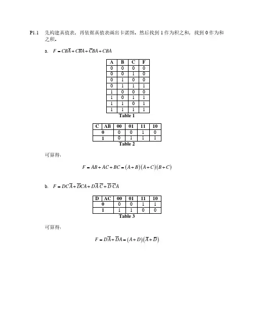
《数字电子技术基础》课后习题答案《数字电路与逻辑设计》作业教材:《数字电子技术基础》(高等教育出版社,第2版,2012年第7次印刷)第一章:自测题:一、1、小规模集成电路,中规模集成电路,大规模集成电路,超大规模集成电路5、各位权系数之和,1799、01100101,01100101,01100110;11100101,10011010,10011011二、1、×8、√10、×三、1、A4、B练习题:1.3、解:(1) 十六进制转二进制: 4 5 C0100 0101 1100二进制转八进制:010 001 011 1002 13 4十六进制转十进制:(45C)16=4*162+5*161+12*160=(1116)10所以:(45C)16=(10001011100)2=(2134)8=(1116)10(2) 十六进制转二进制: 6 D E . C 80110 1101 1110 . 1100 1000二进制转八进制:011 011 011 110 . 110 010 0003 3 3 6 . 6 2十六进制转十进制:(6DE.C8)16=6*162+13*161+14*160+13*16-1+8*16-2=(1 758.78125)10所以:(6DE.C8)16=(011011011110. 11001000)2=(3336.62)8=(1758.78125)10(3) 十六进制转二进制:8 F E . F D1000 1111 1110. 1111 1101二进制转八进制:100 011 111 110 . 111111 0104 3 7 6 . 7 7 2十六进制转十进制:(8FE.FD)16=8*162+15*161+14*160+15*16-1+13*1 6-2=(2302.98828125)10所以:(8FE.FD)16=(100011111110.11111101)2=(4376.772)8=(2302.98828125)10(4) 十六进制转二进制:7 9 E . F D0111 1001 1110 . 1111 1101二进制转八进制:011 110 011 110 . 111 111 0103 6 3 6 . 7 7 2十六进制转十进制:(79E.FD)16=7*162+9*161+14*160+15*16-1+13*16 -2=(1950. 98828125)10所以:(8FE.FD)16=(011110011110.11111101)2=(3636.772)8=(1 950.98828125)101.5、解:(74)10 =(0111 0100)8421BCD=(1010 0111)余3BCD (45.36)10=(0100 0101.0011 0110)8421BCD=(0111 1000.0110 1001 )余3BCD(136.45)10=(0001 0011 0110.0100 0101)8421BCD=(0100 0110 1001.0111 1000 )余3BCD (374.51)10=(0011 0111 0100.0101 0001)8421BCD=(0110 1010 0111.1000 0100)余3BCD1.8、解(1)(+35)=(0 100011)原= (0 100011)补(2)(+56 )=(0 111000)原= (0 111000)补(3)(-26)=(1 11010)原= (1 11101)补(4)(-67)=(1 1000011)原= (1 1000110)补第二章:自测题:一、1、与运算、或运算、非运算3、代入规则、反演规则、对偶规则二、2、×4、×三、1、B3、D5、C练习题:2.2:(4)解:Y=AB̅+BD+DCE+A̅D=AB̅+BD+AD+A̅D+DCE=AB̅+BD+D+DCE=AB̅+D (B +1+CE ) =AB̅+D (8)解:Y =(A ̅+B ̅+C ̅)(D ̅+E ̅)̅̅̅̅̅̅̅̅̅̅̅̅̅̅̅̅̅̅̅̅̅̅̅̅̅̅(A ̅+B ̅+C ̅+DE ) =[(A ̅+B ̅+C ̅)̅̅̅̅̅̅̅̅̅̅̅̅̅̅̅̅+(D ̅+E ̅)̅̅̅̅̅̅̅̅̅̅](A ̅+B ̅+C ̅+DE ) =(ABC +DE )(ABC ̅̅̅̅̅̅+DE ) =DE 2.3:(2)证明:左边=A +A ̅(B +C)̅̅̅̅̅̅̅̅̅̅̅̅ =A +A ̅+(B +C)̅̅̅̅̅̅̅̅̅̅=A +B̅C ̅ =右式所以等式成立(4)证明:左边= (A̅B +AB ̅)⨁C = (A̅B +AB ̅)C ̅+ (A ̅B +AB ̅)̅̅̅̅̅̅̅̅̅̅̅̅̅̅̅C = (A ̅BC ̅+AB ̅C ̅)+A ̅B ̅̅̅̅⋅AB̅̅̅̅̅⋅C =A̅BC ̅+AB ̅C ̅+(A +B ̅)(A ̅+B )C =A̅BC ̅+AB ̅C ̅+(AB +A ̅B ̅)C =A̅BC ̅+AB ̅C ̅+ABC +A ̅B ̅C 右边= ABC +(A +B +C )AB ̅̅̅̅⋅BC ̅̅̅̅⋅CA̅̅̅̅ =ABC +(A +B +C )[(A̅+B ̅)(B ̅+C ̅)(C ̅+A ̅)] =ABC +(A +B +C )(A̅B ̅+A ̅C ̅+B ̅+B ̅C ̅)(C ̅+A ̅)=ABC +(A +B +C )(A̅B ̅C ̅+A ̅C ̅+B ̅C ̅+A ̅B ̅) =ABC +AB̅C ̅+A ̅BC ̅+A ̅B ̅C 左边=右边,所以等式成立 2.4(1)Y ′=(A +B ̅C ̅)(A ̅+BC) 2.5(3)Y ̅=A ̅B ̅(C ̅+D ̅)̅̅̅̅̅̅̅̅̅̅̅̅̅̅̅ C ̅D ̅(A ̅+B ̅)̅̅̅̅̅̅̅̅̅̅̅̅̅̅̅ 2.6:(1)Y =AB +AC +BC=AB (C +C̅)+AC (B +B ̅)+BC (A +A ̅) =ABC +ABC ̅+AB ̅C +A ̅BC 2.7:(1)Y =A ̅B ̅+B ̅C ̅+AC +B ̅C 卡诺图如下: B C A 00 0111100 1 1 1111所以,Y=B̅+AC2.8:(2)画卡诺图如下:B C A 0001 11 100 1 1 0 11 1 1 1 1Y(A,B,C)=A+B̅+C̅2.9:(1)画Y(A,B,C,D)=∑m(0,1,2,3,4,6,8)+∑d(10,11,12,13,14)如下:CDAB00 01 11 1000 1 1 1 101 1 111 ×××10 1 ××Y (A,B,C,D )=A̅B ̅+D ̅ 2.10:(3)解:化简最小项式: Y =AB +(A̅B +C ̅)(A ̅B ̅+C ) =AB +(A̅B A ̅B ̅+A ̅BC +A ̅B ̅C ̅+C ̅C ) =AB (C +C̅)+A ̅BC +A ̅B ̅C ̅ =ABC +ABC ̅+A ̅BC +A ̅B ̅C ̅ =∑m (0,3,6,7)最大项式:Y =∏M(1,2,4,5) 2.13:(3)Y =AB̅+BC ̅+AB ̅C ̅+ABC ̅D ̅ =AB̅(1+C ̅)+BC ̅(1+AD ̅) =AB̅+BC ̅ =AB̅+BC ̅̿̿̿̿̿̿̿̿̿̿̿̿ = AB̅̅̅̅̅∙BC ̅̅̅̅̅̅̅̅̅̅̅̅̅̅̅̅技能题:2.16 解:设三种不同火灾探测器分别为A 、B 、C ,有信号时值为1,无信号时为0,根据题意,画卡诺图如下:B C A 00 01 11 10 0 0 0 1 0 1 0 1 1 1Y =AB +AC +BC=AB +AC +BC ̿̿̿̿̿̿̿̿̿̿̿̿̿̿̿̿̿̿̿=AB ̅̅̅̅⋅AC ̅̅̅̅⋅BC ̅̅̅̅̅̅̅̅̅̅̅̅̅̅̅̅̅̅̅̅=(A ̅+B ̅)(A ̅+C ̅)(B ̅+C ̅)̅̅̅̅̅̅̅̅̅̅̅̅̅̅̅̅̅̅̅̅̅̅̅̅̅̅̅̅̅̅̅=A ̅+B ̅̅̅̅̅̅̅̅̅+A ̅+C ̅̅̅̅̅̅̅̅̅+B ̅+C ̅̅̅̅̅̅̅̅̅第三章:自测题:一、1、饱和,截止7、接高电平,和有用输入端并接,悬空;二、1、√8、√;三、1、A4、D练习题:3.2、解:(a)因为接地电阻4.7k Ω,开门电阻3k Ω,R>R on ,相当于接入高电平1,所以Y =A ̅B ̅1̅̅̅̅̅̅=A +B +0=A +B(e) 因为接地电阻510Ω,关门电0.8k Ω,R<R off ,相当于接入高电平0,所以、Y =A +B +0̅̅̅̅̅̅̅̅̅̅̅̅̅=A̅⋅B ̅∙1̅̅̅̅̅̅̅̅̅̅=A +B +0=A +B3.4、解:(a) Y1=A+B+0̅̅̅̅̅̅̅̅̅̅̅̅̅=A+B̅̅̅̅̅̅̅̅(c) Y3=A+B+1̅̅̅̅̅̅̅̅̅̅̅̅̅=1̅=0(f) Y6=A⋅0+B⋅1̅̅̅̅̅̅̅̅̅̅̅̅̅̅̅̅=B̅3.7、解:(a) Y1=A⨁B⋅C=(A̅B+AB̅)C=A̅BC+AB̅C3.8、解:输出高电平时,带负载的个数2020400===IHOHOH I I NG 可带20个同类反相器输出低电平时,带负载的个数78.1745.08===ILOLOL I I NG 反相器可带17个同类反相器3.12EN=1时,Y 1=A , Y 2=B ̅EN=0时,Y 1=A ̅, Y 2=B3.17根据题意,设A为具有否决权的股东,其余两位股东为B、C,画卡诺图如下,BCA00 01 11 100 0 0 0 01 0 1 1 1则表达结果Y的表达式为:Y=AB+AC=AB+AC̿̿̿̿̿̿̿̿̿̿̿̿=AB̅̅̅̅⋅AC̅̅̅̅̅̅̅̅̅̅̅̅̅̅逻辑电路如下:技能题:3.20:解:根据题意,A、B、C、D变量的卡诺图如下:CD AB00 01 11 1000 0 0 0 001 0 0 0 011 0 1 1 110 0 0 0 0Y =ABC +ABD =ABC +ABD ̿̿̿̿̿̿̿̿̿̿̿̿̿̿̿̿=ABC ̅̅̅̅̅̅⋅ABD ̅̅̅̅̅̅̅̅̅̅̅̅̅̅̅̅̅̅̅̅̅̅电路图如下:第四章:自测题:一、2、输入信号,优先级别最高的输入信号7、用以比较两组二进制数的大小或相等的电路,A>B 二、3、√4、√三、5、A7、C练习题:4.1;解:(a) Y =A⨁B +B ̅̅̅̅̅̅̅̅̅̅̅̅̅=A ̅B +AB ̅+B ̅̅̅̅̅̅̅̅̅̅̅̅̅̅̅̅̅̅̅=A ̅B +B ̅̅̅̅̅̅̅̅̅̅̅=A ̅+B̅̅̅̅̅̅̅̅̅=AB ,所以电路为与门。
自我检测题
1.在存储器结构中,什么是“字”什么是“字长”,如何表示存储器的容量
解:采用同一个地址存放的一组二进制数,称为字。
字的位数称为字长。
习惯上用总的位数来表示存储器的容量,一个具有n字、每字m位的存储器,其容量一般可表示为n ×m位。
2.试述RAM和ROM的区别。
解:RAM称为随机存储器,在工作中既允许随时从指定单元内读出信息,也可以随时将信息写入指定单元,最大的优点是读写方便。
但是掉电后数据丢失。
ROM在正常工作状态下只能从中读取数据,不能快速、随时地修改或重新写入数据,内部信息通常在制造过程或使用前写入,
3.试述SRAM和DRAM的区别。
解:SRAM通常采用锁存器构成存储单元,利用锁存器的双稳态结构,数据一旦被写入就能够稳定地保持下去。
动态存储器则是以电容为存储单元,利用对电容器的充放电来存储信息,例如电容器含有电荷表示状态1,无电荷表示状态0。
根据DRAM的机理,电容内部的电荷需要维持在一定的水平才能保证内部信息的正确性。
因此,DRAM在使用时需要定时地进行信息刷新,不允许由于电容漏电导致数据信息逐渐减弱或消失。
4.与SRAM相比,闪烁存储器有何主要优点
解:容量大,掉电后数据不会丢失。
5.用ROM实现两个4位二进制数相乘,试问:该ROM需要有多少根地址线多少根数据线其存储容量为多少
解:8根地址线,8根数据线。
其容量为256×8。
6.简答以下问题:
(1)CPLD和FPGA有什么不同
FPGA可以达到比 CPLD更高的集成度,同时也具有更复杂的布线结构和逻辑实现。
FPGA 更适合于触发器丰富的结构,而 CPLD更适合于触发器有限而积项丰富的结构。
在编程上 FPGA比 CPLD具有更大的灵活性;CPLD功耗要比 FPGA大;且集成度越高越明显;CPLD比 FPGA有较高的速度和较大的时间可预测性,产品可以给出引脚到引脚的最大延迟时间。
CPLD的编程工艺采用 E2 CPLD的编程工艺,无需外部存储器芯片,使用简单,保密性好。
而基于 SRAM编程的FPGA,其编程信息需存放在外部存储器上,需外部存储器芯片 ,且使用方法复杂,保密性差。
(2)写出三家CPLD/FPGA生产商名字。
Altera,lattice,xilinx,actel
7.真值表如表所示,如从存储器的角度去理解,AB应看为地址,F0F1F2F3应看为数据。
表
8.一个ROM 共有10根地址线,8根位线(数据输出线),则其存储容量为。
A.10×8 B.102×8 C.10×82 D.210×8
9.为了构成4096×8的RAM,需要片1024×2的RAM。
A.8片 B.16片 C.2片 D.4片
10.哪种器件中存储的信息在掉电以后即丢失
A.SRAM B.UVEPROM C.E2PROM D.PAL
11.关于半导体存储器的描述,下列哪种说法是错误的。
A.RAM读写方便,但一旦掉电,所存储的内容就会全部丢失
B.ROM掉电以后数据不会丢失
C.RAM可分为静态RAM和动态RAM
D.动态RAM不必定时刷新
12.有一存储系统,容量为256K×32。
设存储器的起始地址全为0,则最高地址的十六进制地址码为 3FFFFH 。
13.PAL是一种的可编程逻辑器件。
A.与阵列可编程、或阵列固定的 B.与阵列固定、或阵列可编程的
C.与、或阵列固定的 D.与、或阵列都可编程的
习题
1.现有如图所示的4×4位RAM若干片,现要把它们扩展成8×8位RAM。
(1)试问需要几片4×4位RAM
(2)画出扩展后电路图(可用少量门电路)。
图
解:(1)用4×4位RAM扩展成8×8位RAM时,需进行字数和位数扩展,故需要4片4×4的RAM
(2)扩展后电路如图:
D D 6D D 4A 0A 1D D 2D D 0
A 2
2.在微机中,CPU 要对存储器进行读写操作,首先要由地址总线给出地址信息,然后发出相应读或写的控制信号,最后才能在数据总线上进行信息交流。
现有256×4位的RAM 二片,组成一个页面,现需4个页面的存储容量,画出用256×4位组成1K ×8位的RAM 框图,并指出各个页面的地址分配。
解:电路连接图如图所示。
从左到右四个页面的地址为: 000H~0FFH ,100H~1FFH ,200H~2FFH ,300H~3FFH 。
D 7D 6D 5D 4D 3D 2D 1
D 0
A 8A 9
A 0~A 3.试用4×2位容量的ROM 实现半加器的逻辑功能,并直接在图中画出用ROM 点阵图实现的半加法器电路。
A
B
S i C i
图
A
B
i S i
C
A
B
i S i
C
解:由于半加器的输出B A B A S i +=
AB C i = 所以ROM 点阵图如图所示。
4.用EPROM 实现二进制码与格雷码的相互转换电路,待转换的代码由I 3I 2I 1I 0输入,转换后的代码由O 3O 2O 1O 0输出。
X 为转换方向控制位,当X =0时,实现二进制码到格雷码的转换;当X =1时,实现格雷码到二进制码的转换。
试求:
(1)列出EPROM 的地址与内容对应关系真值表;
(2)确定输入变量和输出变量与ROM 地址线和数据线对应关系。
解:真值表为:
输入变量和输出变量与ROM 地址线和数据线对应关系如图所示:
32×4 RAM D 3D 2D 1D 0
A 0
A 1A 3A 2X A 4I 3I 2I 1I 0
O 3O 2O 1O 0
5.试分析如图所示PLA 构成电路。
写出F 1、F 2的逻辑表达式。
1
2
图
解:C
A
F+
+
C
=
AB
A
B
C
1
A
=
F+
BC
C
B
A
2
6.试分析如图所示电路。
(1)列出时序PLA的状态表和状态图
(2)简述该时序PLA的逻辑功能。
图
解:(1)根据电路图写出各触发器驱动方程 n n Q Q J 120+=,10=K
n Q J 01=,n n Q Q K 021+= n n Q Q J 012=,n Q K 12=
(2)写出各触发器状态方程
n n n n n n n Q Q Q Q Q K Q J Q 010200000+=+= n n n n n n n n Q Q Q Q Q Q K Q J Q 0120111111+=+=
n n n n n n n n Q Q Q Q Q Q K Q J Q 1201222222+=+=
(3)列出状态表
(4)状态转换图
(5)功能:同步七进制加法计数器。
7.试分析如图所示由PLA 实现的时序电路,列出状态转换表,简述该时序电路的逻辑功能。
Q 0
Q 1
Q 2
X
图
解 (1)根据电路图写出各触发器状态方程:
n n n n n Q Q X Q Q Q 020112+=+
n n n n n n Q Q Q Q Q Q 0120111+=+
n n n n Q X Q Q Q 00210+=+
(2)根据特性方程列出状态真值表,如表所示。
(3)状态转换图
由状态真值表可得电路在X = 0与X = 1时的状态转换图,如图所示。
12Q Q Q X =0
X =1
(4)逻辑功能
当X =0时,该时序电路为6进制加法计数器;当X =1时,该时序电路为5进制加法计数器。
8.观察如图的可编程I/O 模块,要求把此I/O 模块配置成输入管脚,请标出数据输入通道,给出具体的5个配置比特,并给出T 的值。
I/O 引脚
输出信号
输入信号
时钟
使能使能全局请零
时钟三态控制输出反相
三态反相
锁存输出弱上拉
转换
速率
图
解:要将I/O 引脚作为输入引脚,要将输出三态缓冲器输出置成高阻态,弱上拉禁止。
因此可将三态控制T 置1,三态反相置0,弱上拉置0,其余编程位无关。