产品使用说明书(GRZL智能漏电断路器)
- 格式:doc
- 大小:159.05 KB
- 文档页数:8

SERIESR DB5-40系列小型断路器符合标准:G B/T10963.1产品安装使用前,请仔细阅读使用说明书,并妥善保管,以备查阅。
警告1 严禁湿手操作断路器,否则可能发生电击事故。
2 断路器的短路保护特性工厂已经测试,若是在安装或使用过程中必须验证,则应使用经国家有关部门检测合格的专用测试台测试,严禁用负载线直接短路的试验方法,避免人身伤害。
注意1 断路器安装场所应无爆炸危险、无腐蚀性气体,并应注意防潮、防尘、防火、防震动。
2 断路器的过载保护特性已由制造厂整定,在使用过程中不可随意调整,以免影响性能。
3 为了您的安全,请合理选择断路器的短路保护特性要求,并合理配备安装导线。
4 本产品接触板为铜或铜合金,用户接铝导线时请采用铜铝过渡,搪锡或者加装铜接线鼻,以免导致铜、铝直接接触造成电化学腐蚀导致接线松动,接触电阻增大而烧损线路如因接线不合理出现线路烧毁,本公司概不负责,特此警告!5 接线时一定要接紧,且在安装使用一段时间后要再进行紧固,每次的拧紧力矩为(2~2.5)N·m。
6 安装按照产品说明书要求,包括安装方式、进线方式、适用条件、铜导线(铜排)截面积(参考值见附表A)。
-1-1 用途与适用范围RDB5-40小型断路器(以下简称断路器),主要用于交流50Hz(或60Hz),额定工作电压至230V,额定电流至40A,额定短路分断能力不超过4500A的保护配电线路中,作为线路不频繁接通、分断和转换之用,具有过载、短路保护功能。
产品符合:GB/T10963.1标准。
2 正常工作和安装条件2.1 周围空气温度上限不超过+40℃,下限不低于-5℃,且24h平均温度不超过+35℃。
2.2 安装地点海拔高度应不超过2000m。
2.3 大气相对湿度在周围空气温度为+40℃时不超过50%,在较低温度下允许有较高的相对湿度;例如20℃时达90%。
对由于温度变化偶尔产生在产品上的凝露应采取特殊的措施。
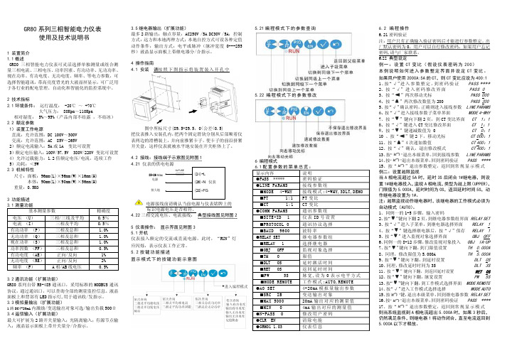
GR80系列三相智能电力仪表使用及技术说明书1 装置简介 1.1概述GR80三相智能电力仪表可灵活选择单独测量或组合测量三相电流、三相电压、功率因素、有功功率、无功功率、视在功率、有功电度、无功电度、频率、等电力参数,可选择智能通讯,带高亮度背光的大液晶屏显示,可广泛用于各行业的配电管理、自动化和智能化的监控系统中。
2 技术指标2.1环境条件: 运行温度: -20℃ ~ +70℃大气压力: 80Kpa~110Kpa相对湿度: 5%~95%(产品内部不结露 ,不结冰) 2.2 额定参数 1)装置工作电源直流:允许范围:DC 100V~300V 交流:允许范围:AC 85V~265V2)额定电流输入:5A 或1A 变比可设置3)额定电压输入:100V/57.5V 380V/220V 变比可设置 4)允许过载能力:1.2倍额定电压/电流,连续工作 5)功耗:<5W 2.3 机械特性尺寸:面板:96mm(L)×96mm(W)×16mm(H) 本体:90mm(L)×90mm(W)×56mm(H) 重量:0.5KG3 功能描述 3.1测量功能基本测量参数 精确度电压 (U) 三相/三线及平均0.5% 电流 (I) 三相及平均 0.5% 有功功率 (P) 三相及总和 1.0% 无功功率 (Q) 三相及总和 1.0% 视在功率 (S) 三相及总和 1.0% 功率因数 (PF) 三相及总和 0.5% 有功电度 (AE) 正向/反向1% 无功电度 (RE)正向/反向 2% 频率 (F) A 相/AB 线电压 0.5%3.2通讯功能(扩展功能)GR80系列自带RS-485通讯口,采用标准的MODBUS 通讯协议,通过通讯口,可以查询全部的测量监控信息。
液晶面板上和背部有LED 指示灯,用于通讯收/发指示。
3.3模拟量输出(扩展功能)1路DC4-20mA 内激励/变送输出对象可选/输出负载500Ω 3.4遥信输入(扩展功能)最大可扩展为2路开关量输入;光隔离输入;有源节点输入;液晶显示面板上带开关量分/合指示。

ZL30791, ZL30795, ZL30793IEEE 1588 & Synchronous EthernetPacket Clock Network SynchronizersProduct BriefAugust 2019 Features•One, Two or Three DPLL Channels•Packet and/or physical-layer frequency, phaseand time synchronization•Physical-layer compliance with ITU-T G.8262,G.8262.1, G.813, G.812, Telcordia GR-1244,GR-253•Packet-timing compliance with ITU-T G.8261,G.8263, G.8273.2 (class A,B,C&D), G.8273.4•Enables 5G wireless applications with sub-100ns time/phase alignment requirements •Programmable bandwidth, 0.1mHz to 470Hz•Hitless reference switching and mode switching •High-resolution holdover averaging•Programmable phase slope limit for transients, downto 1 ns/s•Per-DPLL phase adjustment, 1ps resolution•Input Clocks•Accepts up to 10 differential or CMOS inputs•Any input frequency from 0.5Hz to 900MHz•Per-input activity and frequency monitoring•Automatic or manual reference switching•Fast lock to 1 PPS input, <30 seconds•Any input can be a 1PPS SYNC input for REF+SYNC frequency/phase/time locking •Any input can be a clock with embedded 1PPS •Per-input phase adjustment, 1ps resolution•Output Clock Frequency Generation•Any output frequency from <0.5Hz to 1045MHz (180MHz max for Synth0)•High-resolution fractional frequency conversion with 0ppm error•Synthesizers 1 & 2 have integer and fractional dividers to make a total of 5 frequency families •Output jitter from Synths 1 & 2 is <0.3ps RMS •Output jitter from fractional dividers is typically < 1ps RMS, many frequencies <0.5ps RMS •Each HPOUTP/N pair can be LVDS, LVPECL, HCSL, 2xCMOS, HSTL or programable diff.•Four output banks each with VDDO pin; CMOS output voltages from 1.5V to 3.3V•Per-synthesizer phase adjust, 1ps resolution•Per-output programmable duty cycle•Precise output alignment circuitry and per-output phase adjustment•Per-output enable/disable and glitchlessstart/stop (stop high or low)•Local Oscillator•Operates from a single TCXO or OCXO: 23.75-25MHz, 47.5-50MHz, 114.285-125MHz •Very-low-jitter applications can connect a TCXO or OCXO as the stability reference and a low-jitter XO as the jitter reference•General Features•Automatic self-configuration at power-up from internal Flash memory•Input-to-output alignment <2ns•Internal compensation (1ppt) for local oscillator frequency error in DPLLs and input monitors •Numerically controlled oscillator behavior in each DPLL and each fractional output divider •Programmable Time of Day counters•Easy-to-configure design requires no external VCXO or loop filter components•7 GPIO pins with many possible behaviors•SPI or I2C processor Interface• 1.8V and 3.3V core VDD voltages•Power: 1.3W for 2 inputs, 1 synth, 6 LVDS out •Easy-to-use evaluation/programming software •Factory programmable power-up configuration Applications•Central system timing ICs for SyncE and/or IEEE 1588, SONET/SDH, OTN, wireless basestation and other carrier-grade systems •G.8262/813 EEC/SEC, Telcordia Stratum 2-4Ordering InformationZL30791LFG7 1-Channel 80-lead LGA TraysZL30795LFG7 2-Channel 80-lead LGA TraysZL30793LFG7 3-Channel 80-lead LGA TraysNiAu (Pb-free)Package size: 11 x 11 mm-40︒C to +85︒C1. Block DiagramFigure 1 - Functional Block Diagram2. Application ExampleFigure 2 - Synchronous Ethernet and IEEE 1588 Central Timing ApplicationPACKET_REF[2:0]Register A ccessFracDiv IntDiv FracDivIntDivHP Synthesizer 2low-jitterHPOUT6P HPOUT6N HPOUT7P HPOUT7NDIVREF0P DPLL0R S T _BC S _B _A S E L 0S C K _S C LS O _A S E L 1S I _S D AG P I O [8:0]Microprocessor Port SPI or I2C I/F & GPIO Pins One Diff / Two Single-Ended REF0N REF1P One Diff / Two Single-Ended REF1N REF2P One Diff / Two Single-EndedREF2NREF3P One Diff / Two Single-Ended REF3N REF4P One Diff / Two Single-EndedREF4NReference Monitors & State MachinesDPLL1DPLL2HP Synthesizer 1low-jitterGP Synthesizer 0general purpos eGPOUT0GPOUT1DIV DIVXO Optional x2O S C IO S C OMaster Clock M C L K I N _PDIVHPOUT4P HPOUT4N HPOUT5P HPOUT5N DIV DIVHPOUT0P HPOUT0N HPOUT1P HPOUT1N DIVDIV HPOUT2P HPOUT2N HPOUT3P HPOUT3NDIVDIVM C L K I N _NS R S T _BGPS (1PPS)BITS/SSU Line Extracted Clocks[7:0]TCXODPLL0T4 pathSynth01.544 or2.048MHz CMOS to BITS/SSU1 PPSDPLL1SyncESynth12x 156.25MHz 2x 125MHz155.52MHz, 161.1328125MHz or other frequencyDPLL21588Control info from IEEE 1588 algorithmSynth225MHz 1 PPS or clock w/ embedded PPS 1588 signals to system componentsSyncE signals to system componentsto BITS/SSU systemDPLL1 only present on ZL30795 and ZL30793 DPLL2 only present on ZL307933. Detailed Features3.1 Input Block Features•Ten input reference pins; each can accept a CMOS signal or the POS side of a differential pair; or two can be paired to accept both sides of a differential pair•Any input can be a SYNC signal for REF+SYNC frequency/phase/time locking•Any input can be a clock signal with embedded PPS signal (duty cycle distortion indicates PPS location) •Input clocks can be any frequency from 0.5Hz up to 900MHz (180MHz max for CMOS inputs)•Supported telecom frequencies include PDH, SDH, Synchronous Ethernet, OTN, wireless•Inputs constantly monitored by programmable frequency and single-cycle monitors•Single-cycle monitor can quickly disqualify a reference when measured period is incorrect•Frequency measurement (ppb or Hz) and monitoring (coarse, fine, and frequency-step monitors)•Optional input clock invalidation on GPIO assertion to react to LOS signals from PHYs•Input-to-input phase measurement, 1ps resolution•Input-to-DPLL phase measurement, 1ps resolution•Per-input phase adjustment, 1ps resolution3.2 DPLL Features•One, two or three full-featured DPLLs•Very high-resolution DPLL architecture•State machine automatically transitions among freerun, tracking and holdover states•Revertive or nonrevertive reference selection algorithm•Programmable bandwidth from 0.1mHz to 470Hz•Less than 0.1dB gain peaking•Fast frequency/phase/time lock capability for 1PPS or clock+1PPS input references•Programmable phase-slope limiting (PSL)•Programmable frequency rate-of-change limiting (FCL)•Programmable tracking range (i.e. hold-in range)•Truly hitless reference switching and mode switching•Physical-to-physical reference switching•Physical-to-packet reference switching•Packet-to-physical reference switching•Packet-to-packet reference switching•Per-DPLL phase adjustment, 1ps resolution•High-resolution frequency and phase measurement•Fast detection of input clock failure and transition to holdover mode•High-resolution holdover frequency averaging, better than 0.01ppb when using <10mHz filter•Time-of-Day registers: 48-bit seconds, 32-bit nanoseconds, writeable on input PPS edge3.3 Synthesizer Features•Any-to-any frequency conversion with 0ppm error•Two low-jitter synthesizers (Synth1, Synth2) with very high-resolution fractional scaling (i.e. non-integer multiplication)•Two output dividers per low-jitter synthesizer: one integer (4 to 15 plus half divides 4.5 to 7.5) and one 40-bit fractional•One general-purpose synthesizer (Synth0)• A total of five output frequency families•Easy-to-configure, completely encapsulated design requires no external VCXO or loop filter components3.4 Low-Jitter Output Clock Features•Up to 16 single-ended outputs (up to 8 differential outputs) from Synth1 and Synth2•Each output can be one differential output or two CMOS outputs•Output clocks can be any frequency from 1Hz to 1045MHz (250MHz max for CMOS and HSTL outputs)•Output jitter from Synth1 and Synth2 integer dividers is <0.3ps RMS•Output jitter from fractional dividers is <1ps RMS, many frequencies <0.5ps RMS•In CMOS mode, the HPOUTxN frequency can be an integer divisor of the HPOUTxP frequency (Example 1: HPOUT3P 125MHz, HPOUT3N 25MHz. Example 2: HPOUT2P 25MHz, HPOUT2N 1Hz) •Outputs directly interface (DC coupled) with LVDS, LVPECL, HSTL, HCSL and CMOS components •Supported telecom frequencies include PDH, SDH, Synchronous Ethernet, OTN•Can produce clock frequencies for microprocessors, ASICs, FPGAs and other components•Can produce PCIe clocks•Sophisticated output-to-output phase alignment•Per-synthesizer phase adjustment, 1ps resolution•Per-output phase adjustment•Per-output duty cycle / pulse width configuration•Per-output enable/disable•Per-output glitchless start/stop (stop high or low)3.5 General-Purpose Output Clock Features•Two CMOS outputs from Synth0•Any frequency from 0.5Hz to 180MHz•Output jitter is typically 20-30ps•Useful for applications where the component or system receiving the signal has low bandwidth such asa central timing IC•Can output a clock signal with embedded PPS (ePPS) (duty cycle distortion indicates PPS location) 3.6 Local Oscillator•Operates from a single TCXO or OCXO. Acceptable frequencies: 23.75MHz to 25MHz, 47.5MHz to 50MHz, 114.285MHz to 125MHz. Best jitter: ≥48MHz.•Very-low-jitter applications can connect a TCXO or OCXO (any frequency, any output jitter) as the stability reference and a low-cost low-jitter XO as the jitter reference•This ability to have separate jitter and stability references greatly reduces the cost of the TCXO or OCXO (no jitter requirement, no high-frequency-requirement) and allows reuse of already-qualifiedTCXO and OCXO components3.7 General Features•Automatic self-configuration at power-up from internal Flash memory•Input-to-output alignment <200ps with external feedback•Fast REF+SYNC locking for frequency and 1PPS phase alignment with lower-cost oscillator•Generates output SYNC signals: 1PPS (IEEE 1588), 2kHz or 8kHz (SONET/SDH) or other frequency •JESD204B clocking: device clock and SYSREF signal generation with skew adjustment•Internal compensation for local oscillator frequency error in DPLLs and input monitors, 1ppt resolution •Numerically controlled oscillator (NCO) behavior allows system software to steer DPLL frequency or fractional output divider frequency with resolution better than 0.005ppt•Spread-spectrum modulation available in each fractional output divider (PCIe compliant)•Seven general-purpose I/O pins each with many possible status and control options•SPI or I2C serial microprocessor interface3.8 Evaluation Software•Simple, intuitive Windows-based graphical user interface•Supports all device features and register fields•Makes lab evaluation of the device quick and easy•Generates configuration scripts to be stored in internal Flash memory•Generates full or partial configuration scripts to be run on a system processor•Works with or without an evaluation board4. Software FeaturesThe following figure shows the Time Synchronization Algorithm system environment. The subsections below list the features of the Time Synchronization Algorithm.Host ProcessorTransport Layer ProtocolsMicrosemi ZLS30390IEEE 1588-2008Protocol EngineMicrosemi ZLS30380Time Sync AlgorithmMicrosemiPLLSyncE/Stratum 3/GNSS/IEEE 1588Microsemi Ethernet MAC & PHY(Timestamp)Operating SystemApplication LayerControl, Configuration, Stats & AlarmsPacket NetworkClockPPSTimestamp Reference Clock4.1 Time Synchronization AlgorithmThe Time Synchronization Algorithm is responsible to accurately synchronize the local clock to a selected Server. The Time Synchronization Algorithm is synchronizing the Client to the Server to meet a variety of specifications or applications related to frequency accuracy (FFO), frequency (MTIE, TDEV), phase (1 Hz or 1PPS) and time (UTC & GNSS/GPS).The Time Synchronization Algorithm can run on a variety of host processor architectures, whether embedded into an SoC or on a dedicated small scale CPU (such as Microsemi’s SmartFusion2 SoC FP GA). The Time Synchronization Algorithm will interconnect with a wide array of software-programmable clock generators (such as Microsemi’s Network Synchronizer PLLs), protocol engines (such as Microsemi’s ZLS30390 IEEE 1588-2008 Protocol Engine) and underlying Ethernet MACs and PHYs that perform hardware timestamping.4.2 End Application Target PerformanceThe Time Synchronization Algorithm is suitable for many end application targets, including:• Frequency offset accuracy performance for GSM, WCDMA-FDD, LTE-FDD femtocell, small cell (residential, urban, rural, enterprise), picocell and macrocell applications, with target performance less than ± 15 ppb• Frequency performance for ITU-T G.823 and G.824 synchronization interface, as well as G.8261 PNT EEC, PNT PEC and CES interface specifications•Phase Synchronization performance for WCDMA-TDD, Mobile WiMAX, TD-SCDMA, CDMA2000, LTE-TDD, LTE-A, LTE-A Pro and 5G NR femtocell, small cell (residential, urban, rural, enterprise), picocell and macrocell applications with target performance less than ± 1 μs phase alignment •Time Synchronization for TAI, UTC-traceability and GNSS/GPS replacement4.3 Packet NetworksThe Time Synchronization Algorithm is suitable for high performance over a variety of packet networks including:• ITU-T G.8261 Appendix VI• ITU-T G.8261.1 network limit compliant• ITU-T G.8271.1 network limit compliant without SyncE •ITU-T G.8271.2 network limit compliant•Native Ethernet (switched) & IP (routed) networks•xDSL•Microwave•Fully aware, partially aware and unaware timing supported networks•Networks including intermediate Boundary Clocks and Transparent Clocks•Networks with and without SyncE or frequency physical layer support4.4 Clock SpecificationsThe Time Synchronization Algorithm meets the performance requirements from ITU-T packet clock specifications, or draft packet clock specifications, including:•ITU-T G.8261 Appendix VI•ITU-T G.8263 PEC-S•ITU-T G.8273.2 T-BC full on-path without SyncE•ITU-T G.8273.2 T-BC full on-path with SyncE•ITU-T G.8273.2 T-TSC full on-path without SyncE•ITU-T G.8273.2 T-TSC full on-path with SyncE•ITU-T G.8273.4 T-BC-A (draft)•ITU-T G.8273.4 T-BC-P (draft)•ITU-T G.8273.4 T-TSC-A (draft)•ITU-T G.8273.4 T-TSC-P (draft)4.5 ProfilesThe Time Synchronization Algorithm is suitable for use in a wide variety of markets and applications, including the following IEEE 1588-2008 Profiles:•IEEE 1588 Annex J.3 Delay Request-Response Default Profile (2008)•IEEE 1588 Annex J.4 Peer-to-peer Default Profile (2008)•ITU-T G.8265.1 Telecom Profile for Frequency Synchronization (Edition 1)•ITU-T G.8275.1 Telecom Profile for Phase with Full Timing Support Networks (Edition 1)•ITU-T G.8275.1 Telecom Profile for Phase with Full Timing Support Networks (Edition 2)•ITU-T G.8275.2 Telecom Profile for Phase with Partial Timing Support Networks (Edition 1)•CableLabs CM-SP-RDTI Remote DTI Profile (Edition I0x)•AES 67 Standard for Audio Applications of Networks – High-Performance Streaming Audio-over-IP interoperability: PTP Profile for Media Applications•SMPTE 2095-2 Profile for Use of IEEE-1588 Precision Time Protocol in Professional Broadcast Applications•AES R16 Project Report – PTP parameters for AES67 and SMPTE ST 2059-2 interoperability•IEEE C37.238 Standard Profile for Use of IEEE 1588 Precision Time Protocol in Power System Applications (Edition 2011)•IEEE C37.238 Standard Profile for Use of IEEE 1588 Precision Time Protocol in Power System Applications (Edition 2017)•IEC 61850-9-3 Precision time protocol profile for power utility automation (Edition 1.0)•IEC 62439-3 PTP profiles for high-availability automation networks (Edition 3.0)•IEEE802.1as AVB-TSN gPTP•IEEE 1588-2018 Annex J.5 High Accuracy Profile (based on White Rabbit)•IETF TICTOC Enterprise Profile4.6 Monitoring & RedundancyThe Time Synchronization Algorithm includes monitoring and redundancy for high availability synchronization, including:•Synchronization to the best available server•Client monitoring of secondary server referenceso Monitoring includes full time synchronization reporting of secondary servero Supports a programmable number of secondary server connections•Hitless reference switching between multiple servers•Holdover when server packet connectivity is lost•TIE-clear option to build out, or clear, phase offsets between server references4.7 GeneralThe Time Synchronization Algorithm includes many advanced features to aide in the high-accuracy & high-stability applications, including:•Full PLL state machine (Freerun, Holdover, Frequency Lock Acquiring, Frequency Lock Acquired, Phase Lock Acquired), with programmable thresholds for state transitions•Programmable, non-linear packet selection with PDV suppression•Programmable bandwidth configurability from sub-mHz to 100s of mHz.•Programmable packet rates from 1 packet/second to over 128 packets/second•Programmable phase slope limiting, down to 1 ns/s•Programmable frequency change limiting, down to 1 ppb/s•Warm-start to initialize or seed the Time Synchronization Algorithm from a stored or last-known-good frequency offset to improve convergence•Programmable thresholds for management of phase errors: when to adjust with frequency offsets and when to adjust with phase jumps•User ability to manually add frequency offsets due to temperature or ageing (especially during holdover state)4.8 ReportingThe Time Synchronization Algorithm includes user reporting to aide in performance debugging, including: •Set of user notifications about packet network events, such as packet loss, small transient phase jumps, large transient phase jumps, outliers, network path re-routes•Set of metrics related to the synchronization, such as frequency stability and phase stability•Independent reporting of the forward path and reverse path lock status•Oscillator stability analysis for excessive ageing or temperature variation•Server tracking impairments such as pull-in range exceeded4.9 Product Number SupportThere are several Time Synchronization Algorithm products. The following table provides a summary of support with the ZL3079x devices. Refer to ZLS30380 API User Guide section 1.0 “Products”.Product Number Product Name SupportedZLS30387 Basic Frequency and Phase Support NoZLS30384 IntermediateNoFrequency & PhaseSupportZLS30383 QualcommNoSmall Cell CustomZLS30380 Advanced YesMicrosemi Corporate Headquarters One EnterpriseAliso Viejo, CA 92656 USAWithin the USA: +1 (800) 713-4113 Outside the USA: +1 (949) 380-6100 Sales: +1 (949) 380-6136Fax: +1 (949) 215-4996E-mail: ***************************©2019 Microsemi Corporation. All rights reserved. Microsemi and the Microsemi logo are trademarks of Microsemi Corporation. All other trademarks and service marks are the property of their respective owners. Microsemi Corporation (Nasdaq: MSCC) offers a comprehensive portfolio of semiconductor and system solutions for communications, defense & security, aerospace and industrial markets. Products include high-performance and radiation-hardened analog mixed-signal integrated circuits, FPGAs, SoCs and ASICs; power management products; timing and synchronization devices and precise time solutions, setting the world’s standard for time; voice processing devices; RF solutions; discrete components; security technologies and scalable anti-tamper products; Power-over-Ethernet ICs and midspans; as well as custom design capabilities and services. Microsemi is headquartered in Aliso Viejo, Calif., and has approximately 3,400 employees globally. Learn more at .Microsemi makes no warranty, representation, or guarantee regarding the information contained herein or the suitability of its products and services for any particular purpose, nor does Microsemi assume any liability whatsoever arising out of the application or use of any product or circuit. The products sold hereunder and any other products sold by Microsemi have been subject to limited testing and should not be used in conjunction with mission-critical equipment or applications. Any performance specifications are believed to be reliable but are not verified, and Buyer must conduct and complete all performance and other testing of the products, alone and together with, or installed in, any end-products. Buyer shall not rely on any data and performance specifications or parameters provided by Microsemi. It is the Buyer’s responsibility to independently determine suitability of any products and to test and verify the same. The information provided by Microsemi hereunder is provided “as is, where is” and with all faults, and the entire risk associated with such information is entirely with the Buyer. Microsemi does not grant, explicitly or implicitly, to any party any patent rights, licenses, or any other IP rights, whether with regard to such information itself or anything described by such information. Information provided in this document is proprietary to Microsemi, and Microsemi reserves the right to make any changes to the information in this document or to any products and services at any time without notice.。

智能型万能式断路器使用说明书1.概述1.1适用范围HJW1系列空气断路器(以卜简称断路器)主要适用于交流50Hz,额定工作电压为400V、690V,额定电流为400A-6300A的配电网络中,用来分配电能和保护线路及电源设备免受过载、欠电压、短路取和接地等故障的危害。
断路器核心部件采用智能型控制器,具有精确的选择性保护,可避免不必要的停电,提高供电系统的可靠性、连续性和安全性。
1.2型导及其舍义1 3正常的使用,安装和运输条件1.3.1正常使用条件a)周围空气温度上限不超U+40℃,下限不低于-5℃,24h的平均值不超过+35℃,注:在周围空气温度高于+40℃或低-5℃的条件下使用的断路器应与制造厂协商。
b)安装地点的海拔不超过2000m,c)大气的相对湿度在周围最高温度+40℃时不超过50%,在较低在温度下可以有较高的相对湿度(侧如20℃时的90%),并考虑到因温度变化发生在产品表面上的凝露。
1.3.2正常安装条件a)安装位置应垂直、各方向的倾斜度不超过5℃;b)污染等缎:3级c)安装类别:断路器主电路及欠电压脱扣器线圈、电源变压器初级线圈为Ⅳ级,辅助电路、控制电路为Ⅲ级。
1 3 3正常贮存和运输条件a)温度下限不低于-25℃,上限小超过十55℃,b)相对湿度(25℃时)不超过95%,c)产品在运输过程中,应轻搬轻放,小应倒放,应尽量避免剧烈碰撞。
2.技术特征21分类2.1.1按安装方式分:固定式、抽屉式。
2 1 2按操作方式分:电动操作、手动操作。
2 1 3按脱扣器种类:具有智能型控制器、欠电压瞬时(或延时)脱扣器和分励脱扣器。
2 1 4智能型控制器分娄:a) Perfection-L(简称L)型(经济型,光柱显示),h) Perfection-M(简称M)型(普通型,LED数码显示),c) Perfection-H (简称H)型(增强型,LCD液晶显示)。
2.2主要技术参数见表1表1主要技术参数2 .3主要技术性能2.3. l智能型控制器保护特性的电流整定值范围及准确度见表2。
智能断路器使用说明智能断路器是一种集开关、保护和监控功能于一体的电气装置。
它能够自动感知电路中的电流大小,并根据预设的电流阈值,自动断开或连接电路。
智能断路器采用DC12V电源供电,并具有以下特点和使用说明。
一、特点:1.超低功耗:智能断路器采用先进的芯片技术和节能设计,功耗非常低。
即使连续工作长时间,也不会对电源造成明显影响。
2.自动保护:当电路中的电流超过预设阈值时,智能断路器会自动切断电路,避免过载和短路等危险情况的发生。
3.杜绝火灾隐患:智能断路器内部具有过流保护功能,一旦检测到过大的电流,会迅速切断电路,避免火灾发生。
4.远程监控:智能断路器可以连接到智能家居系统或手机APP,方便用户实时监测和控制电路的运行状态。
5.高可靠性:智能断路器采用优质材料和先进工艺,具有良好的耐用性和可靠性,可长时间稳定运行。
二、使用说明:1.安装:将智能断路器安装在电路中,按照正负极正确连接。
注意电源需要连接DC12V电源。
2.设置电流阈值:根据电路的负载情况,通过旋钮或APP设置智能断路器的电流阈值。
一般根据设备额定电流来设置,确保在电流超过预设值时自动切断电路。
3.实时监控:如果需要实时监控和控制电路的运行状态,可以通过连接到智能家居系统或手机APP来实现。
在APP上可以方便地查看电流大小、开关电路、设置阈值等。
三、注意事项:1.在安装和维修过程中,请务必断开电源,确保安全。
2.请勿超过智能断路器的额定负载,以免造成设备损坏或火灾。
3.定期检查智能断路器的运行状态,确保其正常工作。
4.在使用过程中,注意防潮、防尘,避免影响智能断路器的正常运行。
5.如果长时间不使用智能断路器,建议将其断开电源,以节省能源和延长寿命。
智能断路器是现代电路保护的重要装置,它的智能化和自动化功能,可以提高电路的安全性和稳定性。
使用者在安装和使用时,需要按照说明书进行正确操作,并定期进行检查和维护,以确保电路的正常运行。
RDBXLE系列剩余电流动作断路器符合标准:GB/T 16917.1产品安装使用前,请仔细阅读使用说明书,并妥善保管,以备查阅。
警告1 剩余电流动作断路器(下称漏电断路器)对同时接触被保护电路两线引起的触电危险不能进行保护,使用时请务必注意。
2 漏电断路器进行动作特性试验时,应使用经国家有关部门检测合格的专用测试台,严禁用相线和中性线直接短路或用相线触碰接地装置的试验方法,避免人身伤害。
3 漏电断路器主要功能是对有致命危险的人身触电提供间接接触保护,额定剩余动作电流不超过0.03A的漏电断路器在其他保护措施失效时,也可以作为直接接触电击事故基本防护措施的补充保护措施(不包括对相与相、相与N线间形成的直接接触电击事故的保护),但不能作为唯一的直接接触保护。
4 严禁湿手操作漏电断路器,否则可能发生电击事故。
注意1 漏电断路器安装场所应无爆炸危险、无腐蚀性气体,并应注意防潮、防尘、防震动。
2 漏电断路器安装位置应避开磁场干扰。
3 三极四线和四极漏电断路器的进线N端子必须接入中性线,使电子线路正常工作。
安装时必须严格区分中性线(N)和保护线(P E),经过漏电断路器的中性线不得作为保护线,不得重复接地或接设备外露可导电部分。
保护线不得接入漏电断路器。
4 漏电断路器的漏电、过载、短路保护特性均由制造厂整定,在使用中不可随意调整,以免影响性能。
5 用户不可随意将断路器和剩余电流组件(脱扣器)拼装成漏电断路器来使用。
6 耐压测试本漏电断路器出厂前已按标准规定进行耐压测试。
若安装前-1-必须进行复测确认时,请务必注意:因漏电断路器自带电子组件板,所以,供给电子组件板电源的两极之间不能测试,以避免电子元件损坏。
7 本产品接触板为铜或铜合金,用户接铝导线时请采用铜铝过渡,搪锡或者加装铜接线鼻,以免导致铜、铝直接接触造成电化学腐蚀导致接线松动,接触电阻增大而烧损线路如因接线不合理出现线路烧毁,本公司概不负责,特此警告!铜导线(铜排)截面积(参考值见附表A)。
智能断路器使用操作标准智能断路器指的是一种集电器、电信号判断和控制于一体的自动化设备,用于监视和控制电路中的电压、电流和功率等参数。
智能断路器的使用操作标准非常重要,不仅可以保证使用的安全,还可以延长设备的使用寿命。
下面就介绍智能断路器使用操作标准的相关内容。
一、安装前准备在进行智能断路器的安装前,需要进行以下准备工作:1、巡视安装场地及相关设备,清除现场杂物、灰尘,确保场地干燥且通风良好。
2、检查断路器产品的型号、电压等参数是否与实际需求相符,确认输入功率、输出负载等参数是否符合要求。
3、检查断路器的密封件、接线管、连接螺丝等是否完好无损。
4、在安装前,必须切断电源,在正常情况下禁止现场带电操作,确保人员和设备安全。
5、正确选择和使用工具,如带有保护套的电锤、电钻、扳手等特殊工具。
二、安装过程1、安装位置:智能断路器应安装在非易燃、易爆场所,距地1.8米以上,确保设备使用的通风环境和存放空间;2、安装顺序:先固定底座或安装板,再装饰罩或隔离罩。
3、接线:根据电路原理图将电缆与端子进行连接,严禁错误接线,特别注意接线规则的标准化及其符号的洁净、清晰。
4、测试:在接线完成后,对设备进行耐压检测、电流测量、负载测试等,以确保设备正常运行。
5、标记:安装完成后,应标记设备的型号、电压、额定电流等,以便日后维护和保养。
三、使用过程1、开机前检查:使用前需检查该设备是否处于正常工作状态,无异常声、光现象。
2、开机:开机前确保所有的开关状态为关闭状态,在通电前检查电源线是否正确接线,确认后进行通电。
3、操作规范:在操作过程中,不得超过产品的额定电流。
若设备发生故障,应及时通知专业人员进行检修,严禁私自拆卸。
4、环境要求:使用过程中环境要求偏微湿、无腐蚀性气体、无尘土等污染条件。
5、注意事项:设备在正常使用时,不得超过额定负载水平,避免长时间超载,以免损坏设备。
同时,也要避免轻信传言、随意更换元器件,以免导致故障加重或短路等事故的发生。
O 附录:智能漏电断路器——自动跟踪定档与合闸记忆功能的说明为满足用户的要求,本公司在智能漏电断路器(以下简称漏电断路器)的基础上增设剩余电流自动跟踪定档功能与记忆功能。
该功能是依据基层电力管理部门的建议,为解决线路剩余电流随用电负荷大小变化,以及随季节和天气晴雨变化使用电管理者难以对保护装置的手动动作档位进行合理的设定,无法根据线路实时剩余电流状态使故障接地危险电流在较小的额定动作值下正确保护运行这个难题而开发研制的。
该功能的实现,能科学的、合理的根据线路剩余电流的变化自动确定适当的动作值档位,当线路发生危险的接地故障漏电时,使保护装置在较小的动作值档位下动作,解决了使用管理上的难题,有利于较大地提高剩余电流保护装置的投运率和可靠性,扩大保护面,提高对供电线路剩余电流的安全保护性能。
1、线路剩余电流的变化与自动跟踪定档当漏电断路器剩余动作电流在1000mA,处于自动跟踪定档工作模式时,开机后,会自动把档位设定在1000mA上。
这时如果线路实际剩余电流小于400mA时,1-2分钟漏电断路器就会自动跟踪到800mA,如果线路实际剩余电流小于300mA时,漏电断路器会自动跟踪到600mA时,如果线路实际剩余电流小于200mA。
漏电断路器再会自动跟踪400mA时,如果线路实际剩余电流小于100mA时,漏电断路器再会自动跟踪到200mA时。
在自动跟踪定档下,线路剩余电流突然增加到自动跟踪的设定值时,漏电断路器马上跳闸(如漏电断路器处于600mA自动跟踪定档时,线路剩余电流突然增加到600mA,漏电断路器马上跳闸),20-60s内漏电断路器自动重合闸,重合闸后,漏电断将自动跟踪定档自动升上一档,如果线路剩余电流仍大于比上升后的定档值大,漏电断路器再次跳闸并闭锁(跳死),依此类推。
如果线路剩余电流缓慢增加,漏电断路器同时也能随着线路剩余电流增加而自动上升,一直变换到接近自动跟踪定档的最高档为止。
如果漏电断路器的自动跟踪档档位处于1000mA,线路的剩余电流缓慢下降,那么漏电断路器动作值就会自动下降,随着实际剩余电流的不断缓慢下降,档位会一直降到最低档,即200mA为止。
自动跟踪定档档位动作和不动作值见下表:2、记忆功能当漏电断路器牌合闸工作时,基层电力管理部门根据拨码开关设置说明进行检查记忆数据,便于了解排除线路的故障。
GRZL智能漏电断路器使用说明书1、概述GRZL系列智能漏电断路器的设计思想来源于市场,来源于用户,来源于农网改造第一线,是本公司近年适应我国城乡安全用电实际环境而研制开发的专利产品,使用简便、经济实用、为国内首创。
GRZL系列智能漏电断路器(以下简称漏电断路器),是集剩余电流继电器、漏电断路器及交流接触器的功能于一体的多功能漏电断路器。
适用于三相四线中性点直接接地的低压电网,用来对人身触电解除提供间接接触保护,也可以对线路或用电设备的接地故障、过电流、短路、欠过电压及缺相等进行保护。
2、特点2.1体积小、集漏电断路电器、漏电断路器及交流接触器为一体。
缩小了安装位置,简化了接一。
2.2智能化。
不但具有漏电可选、分断时间可选、过欠压、缺相、过电流、短路、远程辅助控制的保护功能,还具有智能化漏电保护之特点。
主要是漏电电流的数字显示及自动重合闸、动作状态指示等功能,此外,可以设置不同的漏电电流及剩余电流自动跟踪,还可以进行分别显示A相漏电、B相漏电、C相漏电值,当三相漏电不平衡时,可显示三相漏电电矢量和。
2.3能自动记忆运行数据如:合闸次数、总合闸次数、电动合闸次数、重合闸次数、动作/分闸次数、缓变动作次数、超限动作次数、突变动作次数、电动分闸次数、人工分闸次数、电压异常动作次数、电源频率异常次数,区分出主要动作原因及数据记录最近十次如:缓变动作、超限动作、A相突变动作、B相突变动作、C相突变动作、电动分闸、人工分闸、电压异常动作、电源频率异常。
2.4微处理器智能化数字编程控制电路,所有功能均由单片机程序完成。
2.5显示线路剩余电流值,故障漏电跳闸及显示跳闸时剩余电流值。
2.6自动跟踪线路剩余电流,自动调升或降低动作。
2.7矢量保护2.8面板功能及外形、安装尺寸见图1:壳架等级电流外形尺寸安装尺寸A B C D a b 安装孔Φ100A 126 207 150 88 60 188 4孔Φ4250A 145 240 157 102 70 200 4孔Φ4400A/630A 206 360 190 126 102 324 4孔Φ61、安装孔2、电源接线端3、数据显示表4、接通、分断指示标5、指示灯6、手动分闸按钮7、试验按钮8、合闸按钮9、分闸按钮10、功能选择开关3、正常工作气候条件3.1 环境温度:-40℃~+40℃3.2 相对空气湿度:最湿月的平均最低温度不超过25℃时,该月的月平均最大相对湿度不超过90%,并考虑到因温度变化发生在产品表面的凝露。
3.3海拔高度不超过2000米。
3.4污染等级:3级。
3.5安装内别:III3.6安装场所的外磁场在任何方向不超过地磁的5倍。
4、产品型号及含义5、技术参数额定电压:380V220V 三相四线额定频率:50Hz额定电流:63A,100A,160A,200A,250A,400A,630A额定辅助电源电压:220V(进线端左面1接N,进线端右面1接A相)剩余动作电流:1000mA额定漏电动作电流:75mA,100mA,200mA,300mA,500mA,1000mA额定漏电不动作电流:35mA,50mA,100mA,150mA,250mA,500mA剩余电流自动跟踪定档:200mA,400mA,600mA,800mA,1000mA额定分断时间:0.2S,0.3S,0.5S,1.0S(出厂设定在0.3S)延时重合闸:20S~60S欠压动作值单相155V±5%(电压恢复正常后能自动重合闸)过压动作值单相280V±5%(电压恢复正常后能自动重合闸)显示漏电自动跟踪定档值具有自动合闸记忆功能漏电动作值特性分类:AC型额定极限短路分断能力见表1过电流脱扣器保护特性见表2本产品符合:GB14048.2-2008额定极限短路分断能力如下:表1 过电流脱扣器保护特性如下:表2周围空气湿度试验电流脱扣时间状态1.05In2h内不脱扣冷态开始1.30In2h内脱扣热态开始3In可返回时间>2S冷态开始任何合适温度10In<0.2S冷态开始+20℃±2℃ 1.05In2h内不脱扣冷态开始1.30In2h内脱扣热态开始6、安装、试验与使用6.1安装前,必须检查漏电断路器是否处于断开位置(分合闸指示杆突时处于分闸位置),在合闸位置时应手动脱扣!6.2漏电断路器应垂直安装(倾斜度≤5)用螺钉通过安装孔固定。
6.3用户根据负荷选择合适的导线,把导线接入漏电断路器(须配接铜接头)。
漏电断路器的上接线端为主电路的电源端,下接线为出线端。
电源中性(零线)必须接在“N”端子,不接零线或辅助电源相线断相,漏电断路器将不能工作。
6.4安装,接线完毕,向漏电断路器的电源端送电,此时绿色“电源”指示灯亮,红色“分闸”指示灯亮,漏电断路器处于分闸断开状态。
按“合闸”按钮,漏电断路器自动合闸,当漏电断路器处于闭合状态时,只有绿色“电源”指示灯亮。
6.5欠压、过压及缺相跳闸,绿色“电源”指示灯亮,红色“分闸”指示灯亮,同时黄色“欠压、过压”指示灯亮,表示电源电压不正常。
电源电压正常后,黄色“欠压、过压”指示灯熄灭,漏电断路器自动重合闸,恢复正常运行。
6.6在使用中,按试验按钮进行检查漏电断路器是否正常,按按钮后,漏电断路器动作显示“E”或显示漏电电流值(数字)。
6.7漏电电流矢量和超过漏电电流动作值时,漏电断路器立即动作,这时,绿色“电源”指示灯亮,红色“分闸”指示灯亮,红色“漏电”指示灯闪亮,动作后,20S-60S自动重合闸,重合闸后10秒内,漏电电流仍大于漏电动作值,漏电断路器立即动作,这是绿色“电源”指示灯亮,漏电断路器自锁,并不再自动重合闸。
6.8过电流,短路跳闸:绿色“电源”指示灯亮,红色“分闸”指示灯亮,产品不能自动合闸。
6.9按“分闸”按钮,可分断主电路:如果停电后要分断主电路,可用“手动分闸”分断主电路。
在这两种情况下,漏电断路器不重合闸。
6.10漏电断路器安装,接线,试验后,应在线路末端进行试验,正常后再投入运行。
6.11漏电断路器有漏电电流数字显示时,用户应注意漏电电流变化,如果电流较大或变异常时,用户可以采取预防措施。
如果需要检查A、B 、C、三相中每一相的漏电电流,把拨码开关的“5”“6”“7”“8”设置在(拨向上方),此时,“漏电”指示灯闪亮没有保护功能,具体设置参数看(表3)。
检查完毕后,应立即将被码开关设置到正常工作位置!!!拔码开关设置功能表(表3)拔码开关设置说明如下:12345678欠压1位控制上为启用,下为退出过压2位控制上为启用,下为退出分断时间可选(3~4)控制0.2s下下0.3s下上0.5s上下1.0s上上漏电电流可选(6~7~8位)控制75mA上下下100mA上下上200mA上上下300mA下下下500mA下下上1000mA上上上自动跟踪下上上显示自动跟踪值上上上合闸次数及每相漏电电流值(5、6、7、8位)控制总合闸次数上上下下自动重合闸次数上上下上总漏电电流和上下下下A相漏电电流上下上下B相漏电电流上下上下C相漏电电流上下上上产品出厂时额定漏电电流为300mA,漏电分断时间设置为0.3S。
7、漏电断路器数字显示及指示显示主要含义8、故障分析与排除(表4主要故障及排除方法)9、注意事项请用户使用本产品前仔细阅读本《使用说明书》并请妥善保管好本说明书。
9.1 额定漏电电流可先设置及漏电分断时间可先设置见表3.9.2禁止擅自打开漏电断路器,保存好合格证。
9.3漏电断路器对相线与相线、相线与零线之间发生的漏电、触电不能保护。
9.4漏电断路器出线端的零线不能重复接地,被保护线路的任何线不能与其他线路混合使用。
9.5原有的用电设备保护接零必须拆除,改为保护接地。
9.6导线必须用铜拉头后才能接入漏电断路器接线端子,禁止铝导线直接接进接线端子。
9.7漏电断路器因安装和使用不当引起的非质量问题和接线端子因接触不良过热损坏等,不能退换。
本公司可负责维修,费用自理。
9.8漏电断路器在使用中,应按规定每月按试验按钮一次。
检查漏电断路器能否正常动作,并记录。
9.9漏电断路器处于合闸时,当漏电指示灯闪亮,漏电处于退出状态(注:试验按钮是不动作)9.10远程控制功能不需要外接电源。
如遇其它故障,敬请与本公司联系,本公司会尽快给你指导答复或派技术人员前来解决。
10、订货须知用户订货时必须说明:a、漏电断路器名称及型号b、漏电断路器额定脱扣电流(A)c、漏电断路器额定漏电动作电流(mA)d、数量注:漏电断路器如需要远程控制、矢量保护功能、漏电额定值特殊要求敬请注明。