贴片三端陶瓷滤波电容器(EMI,三端滤波器)规格书
- 格式:pdf
- 大小:3.33 MB
- 文档页数:4
陶瓷滤波器及它的三类原理陶瓷滤波器近几年的市场前景看好,因为部分工艺还不成熟,还没有到资本竞争的时候。
明年预计会有一个大爆发。
近5年是陶瓷滤波器发展的黄金期,但是工序长,为保证一致性,自动化水平需要提高,设备的投入将在工艺成熟后,大批量增加。
今天小编来讲讲陶瓷滤波器及其陶瓷滤波器原理。
一,什么是陶瓷滤波器,陶瓷滤波器有什么用什么是陶瓷滤波器陶瓷滤波器是由锆钛酸铅陶瓷材料制成的,把这种陶瓷材料制成片状,两面涂银作为电极,经过直流高压极化后就具有压电效应。
陶瓷滤波器的作用起滤波的作用,具有稳定,抗干扰性能良好的特点,广泛应用于电视机、录像机、收音机等各种电子产品中作选频元件。
它具有性能稳定、无需调整、价格低等优点,取代了传统的LC滤波网络。
陶瓷滤波器的结构陶瓷滤波器的结构有二端和三端两大类。
彩电中的带通滤波器常用型号有LT5.5M、LT6.5M、LT6.5MA、LT6.5MB陶瓷滤波器;调频立体声收录机、收音机常用的10.7MHz中频滤波器有LT10.7MA、LT10.7 MB、LT10.7MC等,调幅收音机的中频滤波器有LT455、LT465等。
彩电中的带阻滤波器(陷波器)常用型号有XT4.43M、XT5.5MA、XT5.5MB、XT6.0MA、XT6.0MB、XT6.5MA、XT6.5MB等。
陶瓷滤波器的种类电容滤波电路,这是最基本的滤波电路;π型RC滤波电路;π型LC滤波电路;电子滤波器电路。
二,陶瓷滤波器的原理是什么?1.单向脉动性直流电压的特点如图1(a)所示。
是单向脉动性直流电压波形,从图中可以看出,电压的方向性无论在何时都是一致的,但在电压幅度上是波动的,就是在时间轴上,电压呈现出周期性的变化,所以是脉动性的。
但根据波形分解原理可知,这一电压可以分解一个直流电压和一组频率不同的交流电压,如图1(b)所示。
在图1(b)中,虚线部分是单向脉动性直流电压U。
中的直流成分,实线部分是UO中的交流成分。
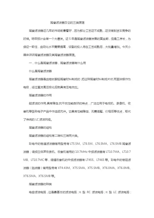
7CFXCA Series(in mm): Input: Output: Ground: ±0.1: ReferenceCFXCD SeriesCFXCE Series(1)(2)(3)(4)(5)Tolerance unless±0.1( ): Input: Output: Ground: Reference(in mm)通信设备用滤波器o kHz SMD型 CFXC_系列干扰: 40dB [在0.1到1.0MHz范围内]输入/输出阻抗: 2000 ohm为安全起见,将滤波器的输出通过一个直流耦合电容与IF放大器相连。
避免直接在陶瓷滤波器的输出端施加电流。
o kHz SMD型 SFPKA系列7通信设备用滤波器为安全起见,将滤波器的输出通过一个直流耦合电容与IF放大器相连。
避免直接在陶瓷滤波器的输出端施加电流。
fn表示标称中心频率为455kHz。
o kHz SMD型 CFUKG系列为安全起见,将滤波器的输出通过一个直流耦合电容与IF放大器相连。
避免直接在陶瓷滤波器的输出端施加电流。
fn表示标称中心频率为455kHz。
o kHz SMD型 CFUKG_X系列7: Input: Output: Ground(1)(2)(3)(4) Tolerance ±0.3mmin mm ()通信设备用滤波器为安全起见,将滤波器的输出通过一个直流耦合电容与IF放大器相连。
避免直接在陶瓷滤波器的输出端施加电流。
fn表示标称中心频率为455kHz。
o kHz SMD型 CFUKF系列为安全起见,将滤波器的输出通过一个直流耦合电容与IF放大器相连。
避免直接在陶瓷滤波器的输出端施加电流。
fn表示标称中心频率为455kHz。
o kHz SMD型 CFWKA系列7Tolerance ±0.3mm in mm : Input : Output : Ground(1)(2)(3)(4)()(1) : Input (2) : Ground(3) : Float (Signal line)(4) : Output ( ) : Reference: EIAJ Monthly Code(in mm)通信设备用滤波器为安全起见,将滤波器的输出通过一个直流耦合电容与IF放大器相连。
1)EMI滤波元件与滤波器的种类滤波器的种类繁多,除了一些传统的电感、电容及其组合外,还有多种新技术产品,其用法各不相同。
根据应用场合不同,可把它们分为三大类:①在交、直流电源部分使用的滤波器:电源滤波器、磁环和磁珠等;②在信号线上使用的滤波器:信号滤波器、磁环和磁珠、穿心电容、滤波连接器(即滤波器阵列)等;③在印刷电路板上使用的滤波器:去耦电容、片状(表面安装式)滤波器、磁珠等。
3)电感器与电感型滤波器线圈与其回流部分就可构成一个传统的电感器,通常有单线圈或多线圈式的。
电感器可按其环绕的磁芯来分类,最常见的两种类型是空气磁芯和磁性磁芯。
磁性磁芯电感器(简称磁芯电感)又可按其磁芯是开路或闭路作进一步分类。
另外,目前广泛应用的铁氧体磁环(或磁珠),虽然在物理概念上讲起变压器的作用,它也更象一个随频率变化的可变电阻,但是人们通常还是把它当作电感器来考虑。
实际应用中的电感器,其绕制导线中必然含有寄生的串联电阻及绕线间的分布电容,因此应用中会在某些频率上产生谐振现象。
衡量电感器性能的主要参数有:分布电容、有效电感、品质因数Q、自谐振频率和饱和电流等。
这些都是应用中应该考虑的。
①普通线圈式电感器具有同样体积和匝数的开路磁芯电感比空气芯电感有大得多的电感量和Q值,闭路磁芯情况会更好。
电感器的一个重要特性是产生杂散磁场和对杂散磁场敏感。
空气芯或开路磁芯电感器最容易引起干扰。
,因为其磁通从电感器扩展到相当大的距离。
就对磁场的敏感度而言,磁芯电感器比空气芯电感器敏感得多,而开路磁芯是最敏感的,因为磁芯(低磁阻通路)集中了外部磁场并引起更多的磁通流过线圈。
普通电感型滤波器一般只用于低频滤波。
在高频条件下,其插入损耗开始降低。
这是因为随着频率的增加,当频率超过电感器的自谐振频率后,寄生电容的阻抗开始降低从而引起电感器的阻抗降低。
这样一来,高频噪声便得不到良好的抑制而通过电感器引起噪声泄漏。
②铁氧体磁环电感器空心铁氧体磁环可以套在导线上,而带引线的铁氧体磁珠则串联在导线中。
Cat.No.C31C-4关于欧盟RoHS指令・本产品目录中的所有产品都符合欧盟RoHS指令。
・欧盟RoHS指令是指欧盟的“关于在电子电气设备中限制使用某些有害物质指令2002/95/EC”。
・详情请参见本公司网站“Murata's Approach for EU RoHS”(/info/rohs.html)。
12345624713646769818592目录本产品目录中的EMIFIL r 、EMIGUARD r 、“EMIFIL”和“EMIGUARD”是村田制作所的注册商标。
EMI静噪滤波器选择指南片状铁氧体磁珠开始BLM41P阻抗值为100MHz时的代表值。
2DLW5BS(AH)DLW31SNFM41PNFA31C2220NFM55PNFE61PNFL21SNFA31GNFA21S开始开始片状EMIFIL r共模扼流线圈3EMI静噪滤波器选择指南品种一览表/有效频率范围4品种一览表/有效频率范围5品种一览表/有效频率范围6..............p.21–91............p.146–148BLM03BLM02BLA31BLM31BLM41BLM18BLM21BLM15BLA2ABL01BL02RN1BL02RN2BL03RN2片状铁氧体磁珠铁氧体磁珠电感器o 片状铁氧体磁珠o 铁氧体磁珠电感器" 片状铁氧体磁珠可在几MHz到几GHz频率范围内有效。
片状铁氧体磁珠作为通用静噪元件,被广泛应用于低噪声控制。
" 片状铁氧体磁珠可在低频范围内产生微小的电感。
但是在高频,电感器的电阻分量将成为主要阻抗。
当串联接入噪声产生电路中时,电感器的电阻性阻抗将阻止噪声传播。
DC用EMI静噪滤波器 (EMIFIL r ) 概要介绍7...............p.95–99p.103–105p.114–120.............p.150–158............p.121–122NFE31P NFE61P/HNFM21P NFM31PNFM21CNFM3DCDS-6DS-9DS-9HNFA31C NFA18S806040201510C=2200pF501005001000 NFM18PNFA21S片状EMIFIL r引线型EMIFIL rT型片状EMIFIL ro片状EMIFIL ro T型片状EMIFIL ro引线型EMIFIL r" 该电容器型EMI静噪滤波器对从几MHz到几百MHz的频率具有大噪声静噪效果。
开关电源输入EMI滤波器设计与仿真摘要:开关电源中常用EMI滤波器抑制共模干扰和差模干扰。
三端电容器在抑制开关电源高频干扰方面有良好性能。
文中在开关电源一般性能EMI滤波器电路结构基础上,给出了使用三端电容器抑制高频噪声的滤波器结构。
并使用PSpice软件对插入损耗进行仿真,给出了仿真结果。
1 开关电源特点及噪声产生原因随着电子技术的高速发展,电子设备种类日益增多,而任何电子设备都离不开稳定可靠的电源,因此对电源的要求也越来越高。
开关电源以其高效率、低发热量、稳定性好、体积小、重量轻、利于环境保护等优点,近年来取得快速发展,应用领域不断扩大。
开关电源工作在高频开关状态,本身就会对供电设备产生干扰,危害其正常工作;而外部干扰同样会影响其正常工作。
开关电源干扰主要来源于工频电流的整流波形和开关操作波形。
这些波形的电流泄漏到输入部位就成为传导噪声和辐射噪声,泄漏到输出部位就形成了波纹问题。
考虑到电磁兼容性的有关要求,应采用EMI电源滤波器来抑制开关电源上的干扰。
文中主要研究的是开关电源输入端的EMI滤波器。
2 EMI滤波器的结构开关电源输入端采用的EMI滤波器是一种双向滤波器,是由电容和电感构成的低通滤波器,既能抑制从交流电源线上引入的外部电磁干扰,还可以避免本身设备向外部发出噪声干扰。
开关电源的干扰分为差模干扰和共模干扰,在线路中的传导干扰信号,均可用差模和共模信号来表示。
差模干扰是火线与零线之间产生的干扰,共模干扰是火线或零线与地线之间产生的干扰。
抑制差模干扰信号和共模干扰信号普遍有效的方法就是在开关电源输入电路中加装电磁干扰滤波器。
EMI滤波器的电路结构包括共模扼流圈(共模电感)L,差模电容Cx和共模电容Cy。
共模扼流圈是在一个磁环(闭磁路)的上下两个半环上,分别绕制相同匝数但绕向相反的线圈。
两个线圈的磁通方向一致,共模干扰出现时,总电感迅速增大产生很大的感抗,从而可以抑制共模干扰,而对差模干扰不起作用。

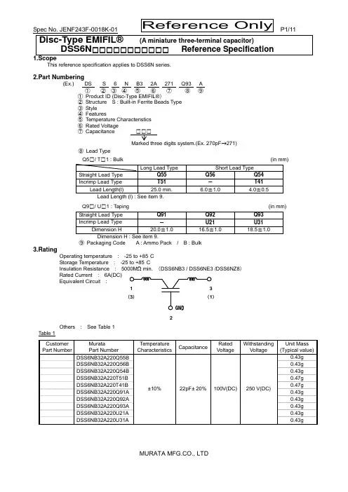
Disc-Type EMIFIL® (A miniature three-terminal capacitor)DSS6N □□□□□□□□□□□ Reference Specification1.ScopeThis reference specification applies to DSS6N series.2.Part Numbering(Ex.) DS S 6 N B3 2A 271 Q93 A ① ② ③ ④ ⑤ ⑥ ⑦ ⑧ ⑨① Product ID (Disc-Type EMIFIL®)② Structure S : Built-in Ferrite Beads Type ③ Style ④ Features⑤ Temperature Characteristics ⑥ Rated Voltage⑦ Capacitance□□□Marked three digits system.(Ex. 270pF →271)⑧ Lead TypeQ5□/ T □1 : Bulk (in mm) Q9□/ U □1 : Taping (in mm) Straight Lead Type Q91 Q92 Q93 Incrimp Lead Type - U21 U31Dimension H 20.0±1.0 16.5±1.0 18.5±1.0 Dimension H : See item 9.⑨ Packaging Code A : Ammo Pack / B : Bulk3.RatingOperating temperature : -25 to +85°CStorage Temperature : -25 to +85°C Insulation Resistance : 5000M Ω min. (DSS6NB3 / DSS6NE3 /DSS6NZ8) Rated Current : 6A(DC) Equivalent Circuit :Others : See Table 1Table 1CustomerPart NumberMurata Part Number Temperature CharacteristicsCapacitanceRated VoltageWithstanding Voltage Unit Mass (Typical value)DSS6NB32A220Q55B ±10% 22pF± 20%100V(DC)250 V(DC)0.43g DSS6NB32A220Q56B 0.43g DSS6NB32A220Q54B 0.43g DSS6NB32A220T51B 0.47g DSS6NB32A220T41B 0.47gDSS6NB32A220Q91A 0.43g DSS6NB32A220Q92A 0.43g DSS6NB32A220Q93A 0.43g DSS6NB32A220U21A 0.43gDSS6NB32A220U31A0.43gGND 1(3)3(1)2Customer Part NumberMurataPart NumberTemperatureCharacteristics CapacitanceRatedVoltageWithstandingVoltageUnit Mass(Typical value) DSS6NB32A330Q55B±10%33pF± 20%100V(DC)250 V(DC)0.43g DSS6NB32A330Q56B 0.43g DSS6NB32A330Q54B 0.43g DSS6NB32A330T51B 0.47g DSS6NB32A330T41B 0.47g DSS6NB32A330Q91A 0.43g DSS6NB32A330Q92A 0.43g DSS6NB32A330Q93A 0.43g DSS6NB32A330U21A 0.43g DSS6NB32A330U31A 0.43g DSS6NB32A470Q55B47pF± 20%0.42g DSS6NB32A470Q56B 0.42g DSS6NB32A470Q54B 0.42g DSS6NB32A470T51B 0.46g DSS6NB32A470T41B 0.46g DSS6NB32A470Q91A 0.42g DSS6NB32A470Q92A 0.42g DSS6NB32A470Q93A 0.42g DSS6NB32A470U21A 0.42g DSS6NB32A470U31A 0.42g DSS6NB32A101Q55B100pF±20%0.42g DSS6NB32A101Q56B 0.42g DSS6NB32A101Q54B 0.42g DSS6NB32A101T51B 0.46g DSS6NB32A101T41B 0.46g DSS6NB32A101Q91A 0.42g DSS6NB32A101Q92A 0.42g DSS6NB32A101Q93A 0.42g DSS6NB32A101U21A 0.42g DSS6NB32A101U31A 0.42g DSS6NB32A151Q55B150pF±20%0.42g DSS6NB32A151Q56B 0.42g DSS6NB32A151Q54B 0.42g DSS6NB32A151T51B 0.46g DSS6NB32A151T41B 0.46g DSS6NB32A151Q91A 0.42g DSS6NB32A151Q92A 0.42g DSS6NB32A151Q93A 0.42g DSS6NB32A151U21A 0.42g DSS6NB32A151U31A 0.42gDSS6NB32A221Q55B220pF±20% 0.42gDSS6NB32A221Q56B 0.42g DSS6NB32A221Q54B 0.42g DSS6NB32A221T51B 0.46g DSS6NB32A221T41B 0.46g DSS6NB32A221Q91A 0.42g DSS6NB32A221Q92A 0.42g DSS6NB32A221Q93A 0.42g DSS6NB32A221U21A 0.42g DSS6NB32A221U31A 0.42gCustomer Part NumberMurataPart NumberTemperatureCharacteristics CapacitanceRatedVoltageWithstandingVoltageUnit Mass(Typical value) DSS6NB32A271Q55B±10%270pF±20%100V(DC)250 V(DC)0.42gDSS6NB32A271Q56B 0.42g DSS6NB32A271Q54B 0.42g DSS6NB32A271T51B 0.46g DSS6NB32A271T41B 0.46g DSS6NB32A271Q91A 0.42g DSS6NB32A271Q92A 0.42g DSS6NB32A271Q93A 0.42g DSS6NB32A271U21A 0.42g DSS6NB32A271U31A 0.42gDSS6NB32A471Q55B470pF±20% 0.43gDSS6NB32A471Q56B 0.43g DSS6NB32A471Q54B 0.43g DSS6NB32A471T51B 0.47g DSS6NB32A471T41B 0.47g DSS6NB32A471Q91A 0.43g DSS6NB32A471Q92A 0.43g DSS6NB32A471Q93A 0.43g DSS6NB32A471U21A 0.43g DSS6NB32A471U31A 0.43gDSS6NB32A102Q55B1000pF±20% 0.42gDSS6NB32A102Q56B 0.42g DSS6NB32A102Q54B 0.42g DSS6NB32A102T51B 0.46g DSS6NB32A102T41B 0.46g DSS6NB32A102Q91A 0.42g DSS6NB32A102Q92A 0.42g DSS6NB32A102Q93A 0.42g DSS6NB32A102U21A 0.42g DSS6NB32A102U31A 0.42g DSS6NE32A222Q55B± 2055 %2200pF±8020%0.42gDSS6NE32A222Q56B 0.42g DSS6NE32A222Q54B 0.42g DSS6NE32A222T51B 0.46g DSS6NE32A222T41B 0.46g DSS6NE32A222Q91A 0.42g DSS6NE32A222Q92A 0.42g DSS6NE32A222Q93A 0.42g DSS6NE32A222U21A 0.42g DSS6NE32A222U31A 0.42g DSS6NZ82A103Q55B± 3085%10000pF±30 %0.42gDSS6NZ82A103Q56B 0.42g DSS6NZ82A103Q54B 0.42g DSS6NZ82A103T51B 0.46g DSS6NZ82A103T41B 0.46g DSS6NZ82A103Q91A 0.42g DSS6NZ82A103Q92A 0.42g DSS6NZ82A103Q93A 0.42g DSS6NZ82A103U21A 0.42g DSS6NZ82A103U31A 0.42g4.Testing Conditions<Unless otherwise specified> <In case of doubt> Temperature : Ordinary Temperature 15 to 35°C Temperature: 20 ± 2°CHumidity : Ordinary Humidity 25 to 85 %(RH) Humidity : 60 to 70 %(RH)Atmospheric Pressure : 86 to 106 kPa 5.Style and DimensionSee item 9.6.Marking7.PerformanceNo. Item Specification TestMethod7.1 AppearanceandDimensions Meet item 9. Visual Inspection and measured with SlideCalipers.7.2 Marking Marking is able to be read easily. Visual Inspection.7.3 CapacitanceandToleranceMeet item 3. Table 27.4 InsulationResistance(I.R.) Meet item 3. Test Voltage : Rated VoltageTime : 1 minute through a suitable resistor 1MΩ.7.5 WithstandingVoltage Products shall not be damaged. Test Voltage : 2.5 times for Rated VoltageTime : 1 to 5 secondsCharge Current : 10 mA max.It shall be applied between input / output terminaland ground terminal.7.6 TemperatureCharacteristics Meet item 3. Capacitance shall be measured at each stepspecified in Table 3 after reaching the thermalequilibrium.The capacitance change against the capacitanceat step 3 shall be calculated.( ) is for DSS6NZ82A103.Table37.7 Solderability Along the circumference of terminalshall be covered with new solder atleast 75%. Flux : Ethanol solution of rosin,25(wt)%(dipped for 5 to 10 seconds)Pre-heat : 150±10℃, 60~90 sSolder : Sn-3.0Ag-0.5CuSolder Temperature 245±5℃Immersion Time : 2 ± 0.5 secondsImmersion Depth :2 to 2.5 mm from the bottom of the body. Frequency TestVoltage Capacitance1±0.1MHz 3 V(rms) max. 22pF~100pF1±0.1kHz 3 V(rms) max. 150pF~10000pFStep 1 2 3 4 5 Temp.(°C)+20±2-25±2(-10)+20±2 +85±2(60)+20±2No. Item Specification TestMethod7.8 ResistancetoSoldering Heat Meet Table 4.Table 4Flux : Ethanol solution of rosin,25(wt)%(dipped for 5 to 10 seconds)Pre-heat : 150±10℃, 60~90 sSolder : Sn-3.0Ag-0.5CuSolder Temperature : 270 ± 5 °CImmersion Time : 3± 0.5 secondsImmersion Depth :1.6 ± 0.7 mm from the bottom of the body.Then measured after exposure in the roomcondition for 4 to 24hours.Appearance Nodamaged.CapacitanceChangeB3 within ± 5%E3 within ± 15%Z8 within ± 20%WithstandingVoltageNo damaged.7.9 Humidity MeetTable5.Table 5 Temperature : 40 ± 2°CHumidity : 90 to 95 %(RH)Time : 500 hours(+24-0 hours)Then measured after exposure in the room condition for 4 to 24hours.Appearance Nodamaged.Capacitance Change B3 within ± 10% E3, within ± 20% Z8 within ± 30%Insulation Resistance B3,E3Z81000MΩ min.7.10 Humidity Life Meet Table6.Table 6 Temperature : 40 ± 2°CHumidity : 90 to 95 %(RH)Time : 500 hours(+24-0 hours)Applying Voltage : Rated VoltageCharge Current : 10 mA max.Then measured after exposure in the room condition for 4 to 24hours.7.11 Heat Life Meet Table 7.Table 7 Temperature : 85 ± 3°CTime : 1000 hours(+48-0 hours)Applying Voltage :B3,E3 character : 2 times of DC rated voltage Z8character : 1.5times of DC rated voltage Charge Current : 10 mA max.Then measured after exposure in the room condition for 4 to 24hours.Appearance No damaged.Capacitance Change B3 within ± 10% E3 within ± 20% Z8 within ± 30%Insulation Resistance B3,E3Z8500MΩ min.Appearance Nodamaged.Capacitance Change B3 within ± 10% E3 within ± 20% Z8 within ± 30%Insulation Resistance B3,E3Z8 1000MΩ min.8.Mounting HoleBulk Taping9.Style and Dimension(1) Bulk(Straight Lead Type) : Q5□*1.Bottom of dielectric may be exposed. *2.There should not be the exposureof the ferrite bead if a hole is on the top of ferrite bead.(in mm)(2) Bulk (Incrimp Lead Type) : T □1*1.Bottom of dielectric may be exposed. *2.There should not be the exposure of the ferrite bead if a hole is on the top of ferrite bead.(in mm)(3) Taping(Straight Lead Type) : Q9□(All symbols in the illustrations below are described in Table 8)(in mm)*1.Bottom of dielectric may be exposed.*2.There should not be the exposure of the ferrite bead if a hole is on the top of ferrite bead.Lead Type l Q55 25.0 min. Q56 6.0±1.0 Q544.0±0.5 in m m Lead Type l T51 25.0 min. T41 4.0±0.5 8.0max.*1φ0.6F15.0±0.5F1lF1=2.5±0.5M arking side Marking side2.54m ax.*27.0m a x .1 2 3(3) (1) 8.0m ax.*1φ0.6F15.0±0.5F110.0m a x .lF1=2.5±0.5M arking sideMarking side2.54m ax.1.0±0.2Detail of form ing*21 2 3(3) (1)t 2t 1(4) Taping (Incrimp Lead Type) : U □1*1.Bottom of dielectric may be exposed.*2.There should not be the exposure of the ferrite bead if a hole is on the top of ferrite bead. Table 8Code Description DimensionsRemarkP Pitch of Component12.7 Product Inclination∆S Determines Crossing P 0 Pitch of Sprocket Hole12.7±0.2 P 1Length from Hole Center to Lead 3.75±0.7P 2Length from Hole Centerto Component Center 6.35±1.3Shift In TapeIn Direction of Feed D Width of Body7.0 max.∆SDeviation along tape, Left or Right 0±1.0W Carrier Tape Width 17.0±0.5W 1 Position of Sprocket Hole 9.0+0,-0.5 Tape Widthwise Shift l Protrusion Length +0.5 ~ -1.0 D 0 Diameter of Sprocket Hole φ4.0±0.1 d Lead Diameter φ 0.6t 1 Total Tape Thickness 0.7±0.2 Includes Thickness of Bonding Tapet 2 Total Thickness,Tape and Lead Wire 1.5 max. ∆h 1 Deviation across Tape,front 1.0 max.∆h 2 Deviation across Tape,rear 1.0 max. L Portion to Cut in Case of Defect 11.0+0,-1.0 W 0 Hold Down Tape Width 12.0±0.5 W 2 Hold Down Tape Position1.5±1.5H Lead length between sprocket hole and forming positionQ91 20.0±1.0 Q92U2116.5±1.0 Q93U3118.5±1.0F Lead Spacing 5.0+0.7,-0.2F 1 2.5+0.4,-0.2(in mm)t 2t 110.Taping10.1 Supplement condition of taping(1) A maximum of 0.3% of the components quantity per reel or Ammo pack may be missing without consecutive missing components.(2) The adhesive power of the tape shall have over 2.94N at the following condition.(3) Splicing method of tape1. Carrier tapeCarrier tape shall be spliced by cellophane tape. Overall thickness shall be less than 1.05 mm.(in mm)2. Hold down tapeHold down tape shall be spliced with overlapping. Overall thickness shall be less than 1.05 mm.(in mm)3. Both carrier tape and hold down tapeBoth tapes shall be cut zigzag and spliced with splicing tape.11. Packing11.1 Packing quantityThe standard packing quantity is as follows.(The packing quantity may be changed due to a fraction of order.)Minimum Packing Form and QuantityTerminal Configuration A Unit Quantity Bulk : in a plastic bag Taping : in an ammo pack * Standard Quantityin a container(corrugated cardboard box)BulkLong Lead Type (Q55/T51) 250 pcs. 5000 pcs.Short Lead Type (Q54/Q56/T41)500 pcs.10000 pcs.Taping (Q91/ Q92/ Q93/U21/U31) 2000 pcs.20000 pcs.* A quantity in a container is depending on a quantity of an order.11.2 Packing Form(1) Bulk<A plastic bag pack>1.Products are packed into a plastic bag.2.The plastic bags are put into a container(corrugated cardboard box) depending on aquantity of an order.F 2.94N Direction of feed Direction of feeda plastic bagcontainer labela containerthe plastic bag with products(2) Taping<An ammo pack>1 .Folding the tape per 25 pitches,products are packed into an ammo package so that each product of each layer wound zigzag is put on top of one another. [Fig 1]2. The dimensions of the ammo package are indicated in [Fig 2].3. The ammo packages are put into a container (corrugated cardboard box) depending on a quantity of an order.4. Not less than 3 consecutive of component shall be missing on both edge of tape.[Fig 1] [Fig 2]The unloading direction : RightThe hold down tape : Upper (in mm) The product body : Left along the unloading direction12.Marking on package12.1 Unit PackageBulk : Marked on a plastic bag.Taping : Marked on a label stuck on an ammo package.Marking on a unit package consists of :Customer part number , MURATA part number, Inspection number(*1), RoHS marking (*2), Quantity, etc*1) « Expression of Inspection No. » □□ OOOO ⨯⨯⨯(1) (2) (3)(1) Factory Code(2) Date First digit : Year / Last digit of year Second digit : Month / Jan. to Sep. → 1 to 9, Oct. to Dec. → O,N,DThird, Fourth digit : Day(3) Serial No.*2) « Expression of RoHS marking »ROHS – Y (△)(1) (2)(1) RoHS regulation conformity parts. (2) MURATA classification number12.2 ContainerMarking on the label stuck on a container consists of :Customer name Purchasing Order Number, Customer Part Number, MURATA part number, RoHS marking (*2), Quantity, etc13.△!Caution13.1 Mounting holesMounting holes should be designed as specified in this specifications.Or different design from this specifications may cause cracks in ceramics which may lead to smoking / firing.13.2 Caution for the product angle adjust workTake care not to apply any mechanical stress to product body at the lead terminal bending process for productangle adjustment after insertion.13.3 Limitation of ApplicationsPlease contact us before using our products for the applications listed below which require especially high reliability for the prevention of defects which might directly cause damage to the third party's life, body or property. (1) Aircraft equipment (7) Traffic signal equipment (2) Aerospace equipment (7) Disaster prevention / crime prevention equipment (3) Undersea equipment (9) Data-processing equipment(4) Power plant control equipment (10) Applications of similar complexity and /or reliability requirements (5) Medical equipment to the applications listed in the above (6) Transportation equipment (vehicles, trains, ships, etc.)zigzag label340max.240m ax.51m ax.14. Notice14.1 Soldering(1) Use rosin-based flux. Do not use strong acidic flux with halide content exceeding 0.2(wt)% (chlorine conversion value). Use Sn-3.0Ag-0.5Cu solder(2) Standard flow soldering profile.Solder temperature Soldering time 250~260 °C 4~6s(3) Resistance to soldering iron goes in the following condition that tip temperature is 350 °C max. andsoldering time is 5 s max.(4) Products and the leads should not be subjected to any mechanical stress during soldering process.(and also while subjected to the equivalent high temperature.)14.2 CleaningProducts shall be cleaned on following conditions.(1) Cleaning Temperature: 60℃ max.(40℃ max. for Isopropyl alcohol).(2) Ultrasonic cleaning shall comply with the following conditions, avoiding the resonance phenomenon at the mounted products and P .C.B.Power :20W / l max.Frequency :28kHz 40kHz Time :5 minutes max.(3) Cleaning agent1. alcohol cleaning agents.・Isopropyl alcohol (IPA)2. Aqueous cleaning agent・Pine Alpha ST-100S(4) Ensure that residual flux and residual cleaning agent is completely removed.Products should be thoroughly dried after aqueous agent has been removed with de-ionized water. (5) For other cleaning methods, please contact Murata engineering.14.3 Operating Environment(1) Do not use products in corrosive gases such as chlorine gas, acid or sulfide gas.(2) Do not use products in the environment where water, oil or organic solvents may adhere to products.(3) Do not adhere any resin to products, coat nor mold products with any resin (including adhesive)to preventmechanical and chemical stress on products.14.4.Storage and handling requirements.(1) Storage periodUse the products within 12 months after delivered.Solderability should be checked if this period is exceeded. (2) Storage environment conditionTo prevent products quality deterioration, stored conditions should be controlled as follows ; 1. Temperature : -10 to 40 degrees centigrade 2. Humidity : 15 to 85% relative humidity3. Products should be stored without sudden changes in temperature and humidity. Don't keep products in corrosive gases such as sulfur,chlorine gas or acid, or it may cause oxidization of lead terminals resulting in poor solderability.4. Products should be stored on the palette for the prevention of the influence from humidity, dust and so on.5. Products should be stored in the warehouse without heat shock, vibration,direct sunlight and so on. (3) Handling ConditionsCare should be taken when transporting or handling product to avoid excessive vibration or mechanical shock.1minutes min.Soldering tim eSolder tem p.25020015010050T e m p e r a t u r e (°C )Pre -heating(in air)Soldering Gradual Cooling(in air)300Spec No. JENF243F-0018K-01 P11/11 MURATA MFG.CO., LTD Reference Only 15. △!Note (1)Please make sure that your product has been evaluated in view of your specifications with our product being mounted to your product.(2)You are requested not to use our product deviating from the reference specifications.(3)The contents of this reference specification are subject to change without advance notice. Please approve our product specifications or transact the approval sheet for product specifications before ordering.。
三端 mom电容结构
三端MOS电容是一种非常常见的电容结构,通常用于集成电路中。
它由三个电极组成,其中一个是栅极,另外两个是源极和漏极。
这种结构可以用于实现高性能的电容器,常见的用途包括滤波器、
频率选择器和存储电荷等。
从结构角度来看,三端MOS电容的栅极与源漏极之间形成了一
个电容结构。
栅极与源漏极之间的电场可以控制电容器的电荷储存
和释放,因此可以实现对电容器的控制。
这种结构通常被用于集成
电路中的模拟电路和射频应用中。
从工作原理角度来看,三端MOS电容的电容值可以通过调节栅
极与源漏极之间的电压来实现。
当栅极与源漏极之间的电压变化时,电容器的电荷储存和释放也会相应变化。
这种特性使得三端MOS电
容在集成电路中应用广泛,特别是在需要可调电容值的场合。
从应用角度来看,三端MOS电容可以用于实现可调电容器,例
如在射频前端的匹配电路中可以用来调节频率响应。
此外,它还可
以用于实现滤波器和频率选择器等电路。
在模拟集成电路中,三端MOS电容也被广泛应用于模拟信号处理电路中。
总的来说,三端MOS电容结构具有灵活可调的特点,可以在集成电路中实现多种功能,是集成电路设计中常用的元件之一。
EMI滤波器的应用及选择指南一、EMI滤波器的电路结构形式(右图所示):1、C型滤波器C型滤波器由三端电容和穿心电容构成,适合于抑制高频。
C型滤波器两端均可视为低阻抗,接高阻抗源和负载。
2、L型滤波器由一个电感器和一个电容器组成。
这种滤波器可以提供高的输入阻抗,也可提供低的输入阻抗,取决于电路的安装方向。
LT电路适用于高阻抗负载,低阻抗源的情况。
LB电路适用于低阻抗负载,高阻抗源的情况。
3、π型滤波器π型滤波器由一个电感器两个电容器构成。
它的输入端和输出端都呈低阻抗性,因为元件比L型或C型多,故抑制性能要好的多。
但在开关电路中有时会出现“振铃”现象。
4、带瞬变抑制器的π型滤波器这种π型滤波器在其输入端增加了一个瞬变抑制器,它具有较好的高频抑制性能,同时可以防止电压尖峰。
5、T型滤波器这种滤波器包括两个电感器和一个电容器,它的两端都是高阻抗,其插入损耗性能和π型滤波器相似。
但它不易出现“振铃”现象,可用在开关电路中。
6、双T型滤波器(多级滤波器)多级滤波器是为源和负载都为低阻抗的电路设计的高性能滤波器,它们也可用在要求高插入损耗的其他情况。
在滤波器的输入端用一个电感器,有利于与美军标MIL-STD-461D(国军标GJB-151A)的测试装置匹配。
二、各种滤波电路的衰减特性:不同的滤波电路有着不同的滤波特性(见右图)。
一般而言,C 型电路的滤波衰减曲线较平坦,没有明显的拐点,适用于大多数电子设备;L 型电路Pi 型电路和T 型电路的滤波衰减曲线较C 型电路拐点明显,适用于抑制的干扰信号与有用信号频率接近的的场合。
但当工作频率为方波时,要注意这些电路的感性和容性器件的量值要选用恰当,避免一味追求滤波衰减性能,而把有用信号的波形部分衰减,导致设备工作反而不正常。
各种滤波电路滤波特性图一、 E MI 感性和容性器件的选择:滤波电容EMI 滤波器所用电容一般为穿芯式陶瓷电容,穿芯式的结构可有效防止高频信号在输入输出端之间直接耦合,且寄生电感小自谐振频率较高,这种同轴性的、低通高阻的设计组合,在1GHz 的频率范围内,可以提供高效的EMI 抑制。
几种常用的EMI滤波器件介绍
伴随电子技术的高速发展,电磁环境日益恶化,大量的电子设备在这种电磁环境中很难正常工作。
另一方面,电子设备的迅速增加,又进一步导致电磁环境的恶化。
因此,现代电子产品设计技术中,如何选用干扰抑制滤波器件,是我们每一位电子产品设计人员必须面对的问题,本文对此进行了详细的阐述。
1. 穿心电容器- 馈通滤波器
馈通滤波器常用于移动通讯设备、雷达导航等一些高频处理模块中,与屏蔽结构体配合,处理输入或输出的低频信号,是其他形式的电容器不能替代的产品。
现在电子线路的工作频率和周围环境中的电磁干扰频率越来越高,将滤波器安装在线路板上所暴露出的高频滤波不足的问题比较突出。
要想在UHF或更高的频段获得更好的滤波效果,特别是保护屏蔽体不被穿透时,必须使用馈通型滤波器解决。
馈通型滤波器安装在金属面板上,具有很低的接地阻抗,并且利用金属面板隔离滤波器的输入和输出,因此滤波器具有非常好的高频滤波效果。
馈通滤波器的电路结构分为C 型(穿心电容)、L 形(一个穿心电容加一个电感)、T 形(两个电感加一个穿心电容)、π形(两个穿心电容加一个电感)等;滤波器的器件越多,则滤波器的过渡带越短,阻带的插入损耗越大。
其中C 型馈通滤波器一般成为穿心电容器。
图1 穿心电容
任何有引线的电容器的滤波效果都会受到接地电感的限制。
如图1 所示,通过将电容器外表面直接用螺纹或焊接的方式接到金属屏蔽体或面板上构成电容器的接地。
由于地电流分散在中心导体周围360°的范围内,实际上不存。
北京芯联科泰电子有限公司贴片叠层瓷介电容器(SMD贴片电容)详细介绍:贴片电容全称:多层(积层,叠层)片式陶瓷电容器,也称为贴片电容,片容。
英文缩写:MLCC。
基本概述贴片电容(多层片式陶瓷电容器)是目前用量比较大的常用元件,就AVX公司生产的贴片电容来讲有NPO、X7R、Z5U、Y5V等不同的规格,不同的规格有不同的用途。
下面我们仅就常用的NPO、X7R、Z5U和Y5V来介绍一下它们的性能和应用以及采购中应注意的订货事项以引起大家的注意。
不同的公司对于上述不同性能的电容器可能有不同的命名方法,这里我们引用的是AVX公司的命名方法,其他公司的产品请参照该公司的产品手册尺寸贴片电容的尺寸表示法有两种,一种是英寸为单位来表示,一种是以毫米为单位来表示,贴片电容的系列型号有0402、0603、0805、1206、1210、1808、1812、2010、2225、2512,是英寸表示法, 04 表示长度是0.04 英寸,02 表示宽度0.02 英寸,其他类同型号尺寸(mm)英制尺寸公制尺寸长度及公差宽度及公差厚度及公差0402 1005 1.00±0.05 0.50±0.05 0.50±0.050603 1608 1.60±0.10 0.80±0.10 0.80±0.100805 2012 2.00±0.20 1.25±0.20 0.70±0.20 1.00±0.20 1.25±0.201206 3216 3.00±0.30 1.60±0.20 0.70±0.20 1.00±0.20 1.25±0.201210 3225 3.00±0.30 2.54±0.30 1.25±0.30 1.50±0.301808 4520 4.50±0.40 2.00±0.20 ≤2.001812 4532 4.50±0.40 3.20±0.30 ≤2.502225 5763 5.70±0.50 6.30±0.50 ≤2.503035 7690 7.60±0.50 9.00±0.05 ≤3.00命名贴片电容的命名所包含的参数有贴片电容的尺寸、做这种贴片电容用的材质、要求达到的精度、要求的电压、要求的容量、端头的要求以及包装的要求。
用于根据实际干扰源设计EMI滤波器的具体参数。
第四章介绍了滤波器是的高频模型及滤波器高频性能的优化,如果设计滤波器时不考虑滤波器元件的高频性能,则设计的滤波器可能达不到理想的性能。
最后介绍了滤波器的设计步骤并设计了一款具有具体参数的EMI滤波器。
关键词:电磁干扰;EMI滤波器;寄生参数ABSTRACTWith the rapid development of electrical technology,electromagnetic compatibility is a hot issue.It is an indispensable part to solve the problem of electromagnetic interference when suppressing conducted interference.EMI filter,as a common method to solve conducted interference,is of great significance to the research of its design.This article first introduces the causes of electromagnetic interference,including external factors and internal factors of power supply.Then the importance of EMC design of EMI filter is introduced.The second chapter introduces the basic principle of EMI filter as the basis of designing EMI filter.The third chapter introduces the test method of conducted interference and the separation method of interference signal,which is used to design the specific parameters of EMI filter according to the actual interference source.The fourth chapter introduces the high frequency model of the filter and the optimization of the high frequency performance of the filter.If the high frequency performance of the filter element is not considered in the design of the filter,the designed filter may not achieve the ideal performance.Finally,the design steps of the filter are introduced and an EMI filter with specific parameters is designed.Keywords:electromagnetic interference;EMI filter;parasitic parameter目录第一章绪论1.1文献综述 (5)1.2研究内容 (8)1.3本论文的结构安排 (8)第二章电磁干扰及EMI滤波器的介绍2.1电磁兼容基本原理 (8)2.1.1电磁干扰三要素 (8)2.1.2干扰信号产生的原因 (9)2.2EMI滤波器的原理 (11)2.2.1EMI滤波器简介 (13)2.2.2滤波器技术指标 (14)2.2.3滤波器结构选取原则 (14)2.3本章小结 (14)第三章传导干扰的测试与分离3.1传导干扰测试系统 (14)3.2本章小结 (16)第四章EMI滤波器的优化设计4.1无源器件的高频模型 (16)4.2EMI滤波器的优化 (20)4.2.1三端电容器的EMI滤波器 (20)4.2.2高频寄生参数的消除 (21)4.3本章小结 (25)第五章设计步骤5.1计算所需衰减量 (25)5.2滤波器截止频率确定 (25)5.3元件参数设计 (26)5.4寄生参数提取 (28)5.5本章小结 (31)第六章EMI滤波器的设计与实现6.1设计实例 (31)6.2本章小结 (32)第七章结论 (33)参考文献 (33)致谢 (34)第一章绪论1.1文献综述EMC设计技术是当下的热门研究问题,主要有两个方面的原因:一是电气设备的工作频率相较于以前有了很大提高,这将增加电路间的互相影响。