风华三端滤波器(三端滤波电容)规格书
- 格式:pdf
- 大小:4.57 MB
- 文档页数:28
广东风华高新科技股份有限公司GUANGDONG FENGHUA ADV ANCED TECHNOLOGY HOLDING CO.,LTD.承认书APPROV AL SHEET客户名称:CUSTOMER品名:常规厚膜片式固定电阻器PARTNAME规格版本号VERSION日期DATE制造客户APPROV AL APPROV AL 拟制审核确认检验审核批准FENGHUAFENG HUA ADV ANCED TECHNOLOGY (HOLDING) CO., LTD序号 No 目 录TABLE OF CONTENTS1.0 概述Summary2.0 结构及尺寸Structure And Dimensions3.0 型号规格表示办法How To Order4.0 电气性能Performance Specification5.0 可靠性Reliability Data6.0 包装Package7.0 环保情况说明 Environmental Protection Statement 8.0 推荐使用的焊接曲线Recommended soldering profile 9.0 使用注意事项Precautions For UseRC/RS□□□□1.0概述Summary片式电阻器主要生产的型号包括01005、0201、0402、0603、0805、1206、1210、2010、2512。
其特点是:The dimension type for chip resistor including01005、 0201、0402、0603、0805、1206、1210、2010、2512, and the features are as below:*体积小、重量轻miniature and light weight*电性能稳定,可靠性高 stable electrical capability and high reliability *机械强度高、高频特性优越superior mechanical and frequency*装配成本低,并与自动贴装设备匹配low assembly cost, suit for automatic SMT *适应再流焊与波峰焊suit for re-flow and wave flow soldering .*符合ROHS指令要求Compliant with ROHS Directive*符合无卤素要求Compliant with halogen free requirement*禁止使用SS-00259中规定的1级环境管理物质*SONY指定原材料只能从绿色伙伴认定供应商处采购产品广泛应用于计算机、通讯、工业自动化、航天航空、军事、数字电视、数字音响及消费类电子等领域。
常规厚膜片式固定电阻器GENERAL CHIP FIXED RESISTOR特长 Features体积小重量轻Miniature and light weight.适应再流焊与波峰焊Suit for reflow and wave flow solder.电性能稳定可靠性高Stable electrical capability, high reliability.装配成本低并与自动Low assembly cost, suit for automatic SMT装贴设备匹配equipment.机械强度高高频特性优越Superior mechanical and frequencycharacteristics.符合RoHS指令要求According with RoHS standard品名构成 Type Designation例Example200ppm/400ppm/200ppm/400ppm/100ppm/0603080512061210181220102512250ppm/Resistance Value Code三位数E-24系列前两位表示有效数字第三位表示有效数字后零的个数Three digits (E-24series): The first two digits are significant figuresand the third one denotes number of zeros.四位数E-96系列前三位表示有效数字第四位表示有效数字后零的个数Four digits (E-96series):The first three digits are significantExample103=10K E-241003=100K E-961R0=1.00.5%1%2%5%10%结构及规格尺寸Construction and dimension单位Unit: mm 型号Type L W t a b 0201 0.600.05 0.300.05 0.230.05 0.100.05 0.150.05 0402 1.000.10 0.500.10 0.300.10 0.200.10 0.250.10 0603 1.600.15 0.800.15 0.400.10 0.300.20 0.300.20 0805 2.000.20 1.250.15 0.500.10 0.400.20 0.400.20 1206 3.200.20 1.600.15 0.550.10 0.500.20 0.500.20 1210 3.200.20 2.500.20 0.550.10 0.500.20 0.500.20 1812 4.500.20 3.200.20 0.550.10 0.500.20 0.500.20 2010 5.000.20 2.500.20 0.550.10 0.600.20 0.600.20 2512 6.400.20 3.200.20 0.550.10 0.600.20 0.600.20产品外观Appearance1.电阻器表面二次玻璃体保护膜覆盖完好且难以脱落,表面平整The surface of resistor is covered with Protective Coating which hard to fade, and the surface of coating should avoid unevenness.2.电阻器引出端电极覆盖均匀镀层较难脱落且平整无裂痕针孔变色The terminal part is covered equable , the plating is hard to fade, and should avoid unevenness, flaw, pinhole and discoloration.3.电阻器芯片无裂痕标志可辨With a clear mark , the resistor body is crack-free.参考标准 Reference StandardGB/T 5729-2003GB/T 9546-1995JIS C 5223-1995JIS C 5201-1998JIS C 5202-1990负荷下降曲线Derating Curve755025使用温度范围OperatingTemperatureRange-55125环境温度Ambient temperature ()当电阻使用的环境温度超过70时其额定负荷(额定电压)按上述曲线下降For resistors operated in ambient over 70,rated load (power rating) shall be derated in accordance with the above figure.额定值 Ratings项目 Item 0201 0402 06030805 1206 1210 1812 20102512常规功率系列Normal PowerSeries1/20W 1/16W1/16W1/10W1/8W 1/4W 1/2W 1/2W1W 额定功率Power Rating提升功率系列Upgraded PowerSeries/ /1/10W1/8W1/4W1/3W/ 3/4W/最大工作电压VMax.Working Voltage25 50 50 150200 200 200 200 200最大过负荷电压VMax.Overload Voltage50 100 100 300400 400 400 400 400电阻温度系数Resistance TemperatureCoefficient10R 1M:200ppm/1R<10,1M<R10M:400ppm/10R1M:100ppm/1R<10,1M<R10M:250ppm/阻值范围Resistance Range1~10ME-24E-96系列阻值误差精度Resistance Tolerance5%10%1~10M: 1%2%5%10%10~1M:0.5%1~10M: 1%2%5%10%10~1M:0.5%1% 2% 5%10% 使用温度范围Operating Temperature Range-55~+125额定温度Rated Temperature70注额定电压=额定功率标称电阻值或最大工作电压两者中的较小值Note Rated Voltage=Power Rating Resistance Value or Max. Working Voltage , whichever is lower.特性 Characteristics项目Item标准Specifications测试方法JIS C 5202标准Test Methods (JIS C 5202)端头强度Bending Strength无可见损伤No mechanical damageR 1.0%R+0.05弯曲速度(Speed):1mm/s弯曲距离(Bending Distance):0201040206030805120612103mm1812201025121mm电阻温度系数T.C.R在规定值内within specified T.C.R测定范围-55~+125Measure between -55~+125温度循环TemperatureCycling无可见损伤No mechanical damageR 1.0%R+0.05-5530分钟~常温5分钟~12530分钟5个循环-5530min~normal temperature5min~12530min 5 cycles短时间过负载Short TimeOverload无可见损伤No mechanical damageR 2.0%R+0.052.5倍额定电压或最大过负荷电压取最小者保持5秒2.5Rated voltage or Max. Overload Voltagewhichever is lower for 5 seconds续上表稳态湿热Steady state humidity无可见损伤No mechanical damage R 3.0%R+0.1 40290~95RH 1000小时 402 90~95RH 1000h70耐久性 Load Life无可见损伤No mechanical damageR 3.0%R+0.17021000小时额定电压通1.5小时/断0.5小时7021000hRated voltage 1.5h on/0.5h off上限类别温度耐久性 Endurance atupper temperature 无可见损伤No mechanical damageR 3.0%R+0.11252 1000h 耐溶剂性Resistance toSolvent无可见损伤 No mechanical damage R 1.0%R+0.05 浸入三氯乙烯 10h 1hDip in chloroethylene for 10h 1h .绝缘电阻Insulation Resistance1000M Min在电极与基片间施加100V 直流电压,保持1分钟,然后测绝缘电阻值.Apply DC 100V between substrate and terminationfor 1 minute, then check insulation resistance .耐焊接热 Resistance toSoldering Heat无可见损伤No mechanical damageR 1.0%R+0.052605 10s 1s 可焊性Solderability 可焊面积95% 95% Cover Min2355 2s 0.5s 附着力Adhesion 外观无可见损伤 No mechanical damage 施加力5N 10s 1s Applying 5N 10s 1s包装 Packaging编带包装 Tape and reel * 纸带编带 Paper taping 020104020603080512061210单位unit: mm 型号Type A B W F E 0201 0.700.1 0.400.1 8.00.20 3.50.05 1.750.10402 1.200.1 0.700.1 8.00.20 3.50.05 1.750.10603 1.850.1 1.100.1 8.00.20 3.50.05 1.750.10805 2.350.1 1.650.1 8.00.20 3.50.05 1.750.11206 3.500.2 1.900.2 8.00.20 3.50.05 1.750.11210 3.500.2 2.800.2 8.00.20 3.50.05 1.750.1单位unit: mm 型号Type P P0 P1 ФD0 T 0201 2.00.05 4.00.1 2.00.05 1.50.1 0.5Max0402 2.00.05 4.00.1 2.00.05 1.50.1 0.6Max0603 4.00.1 4.00.1 2.00.05 1.50.1 0.600.10805 4.00.1 4.00.1 2.00.05 1.50.1 0.750.11206 4.00.1 4.00.1 2.00.05 1.50.1 0.750.11210 4.00.1 4.00.1 2.00.05 1.50.1 0.750.1*塑料带编带 Embossed taping单位unit: mm型号Type A0 B0WFEt 1812 4.800.10 3.400.10 12.000.10 5.500.10 1.750.10 0.250.05 2010 5.450.10 2.770.10 12.000.10 5.500.10 1.750.10 0.240.05 25126.730.10 3.400.10 12.000.10 5.500.10 1.750.10 0.240.05单位unit: mm型号Type PP0P1 ФD0ФD1K0 1812 4.000.10 4.000.10 2.000.05 1.550.10 1.500.10 1.000.10 2010 4.000.10 4.000.10 2.000.05 1.50+0.10/-0 1.500.10 0.840.10 25124.000.10 4.000.10 2.000.051.50+0.10/-0 1.500.100.810.10* 卷盘 Reel单位unit: mm型号Type MWTABCD0201 0402 0603 0805 1206 1210 178 2.09.5 1.012.5 1.52.0 0.513.0 0.521.0 0.558.0 2.01812 2010 2512178 2.013.0 0.515.5 1.52.0 0.513.0 0.521.0 0.557.0 2.0*塑料盒包装Bulk case单位unit:mm包装数量 Packaging quantity包装方法Packagingstyle编带Tape and reel塑料盒Bulk case塑料袋散装Bulk型号Type 020104020603080512061210181220102512020104020603 0805 12061210201018122512020104020603080512061210181220102512数量PCSQuantity10000 5000 4000 50000 25000 10000 5000 1500 1000 50000 10000 4000。
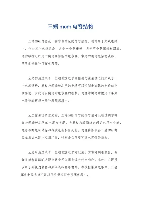
三端 mom电容结构
三端MOS电容是一种非常常见的电容结构,通常用于集成电路中。
它由三个电极组成,其中一个是栅极,另外两个是源极和漏极。
这种结构可以用于实现高性能的电容器,常见的用途包括滤波器、
频率选择器和存储电荷等。
从结构角度来看,三端MOS电容的栅极与源漏极之间形成了一
个电容结构。
栅极与源漏极之间的电场可以控制电容器的电荷储存
和释放,因此可以实现对电容器的控制。
这种结构通常被用于集成
电路中的模拟电路和射频应用中。
从工作原理角度来看,三端MOS电容的电容值可以通过调节栅
极与源漏极之间的电压来实现。
当栅极与源漏极之间的电压变化时,电容器的电荷储存和释放也会相应变化。
这种特性使得三端MOS电
容在集成电路中应用广泛,特别是在需要可调电容值的场合。
从应用角度来看,三端MOS电容可以用于实现可调电容器,例
如在射频前端的匹配电路中可以用来调节频率响应。
此外,它还可
以用于实现滤波器和频率选择器等电路。
在模拟集成电路中,三端MOS电容也被广泛应用于模拟信号处理电路中。
总的来说,三端MOS电容结构具有灵活可调的特点,可以在集成电路中实现多种功能,是集成电路设计中常用的元件之一。
AM/FM收音机的安装与调试实训报告一、实训目的:1、学习收音机的调试与装配。
2、提高读整机电路图及电路板图的能力。
3、掌握收音机生产工艺流程,提高焊接工艺水平。
二、实训容:1、收音机电路原理分析。
2、掌握印制电路板的组装及焊接工艺。
3、进行AM、FM中频及统调覆盖的调试及整机测试。
4、故障判断及排除。
三、实训基本要求:1、会检测元器件并判别其质量。
2、独立完成各测试点的测量与整机安装。
3、会排除在调试与装配过程中可能出现的问题与故障。
四、实训步骤(一)对照元件清单表清点元件(二)元件的插接与焊接(三)收音机的整机调试1、调幅部分的调整①中频放大电路的调整——调AM中周➢调整时,整机置中波AM收音位置➢将音量电位器置于最大位置,将收音机调谐到无电台广播又无其它干扰的地方(或者将可调电容调到最大,即接收低频端)。
➢使高频信号发生器输出载频为465kHz,调制信号频率为1000Hz,调制度为30%的调幅信号接入IC的“10”脚。
➢用无感螺丝刀微微旋转中频变压器(黑色中周)的磁帽向上或向下调整,使示波器显示的波形幅度最大无失真。
在调整中频变压器时也可以用喇叭监听,当喇叭里能听到1000Hz的音频信号,且声音最大,音色纯正,此时可认为中频变压器调整到最佳状态。
②、调整接收围(频率覆盖)——调AM的电感和电容➢调整时,整机置中波AM收音位置。
➢将音量电位器置于最大位置。
低端频率调整:➢将可变电容器(调谐双联)旋到容量最大处,即机壳指针对准频率刻度的最低频端。
➢使高频信号发生器输出载频为515kHz,调制信号频率为1000Hz,调制度为30%的高频调幅信号接入IC的“l0”脚。
➢用无感螺丝刀调整中波振荡线圈的磁芯(红色中周),以改变线圈的电感量,使示波器出现1000Hz波形,并使波形最大。
或直接鉴听收音机的声音,使收音机发出的声音最响最清晰。
高端频率调整:➢将整机的可变电容器置容量最小处,这时机壳指针应对准频率刻度的最高频端。
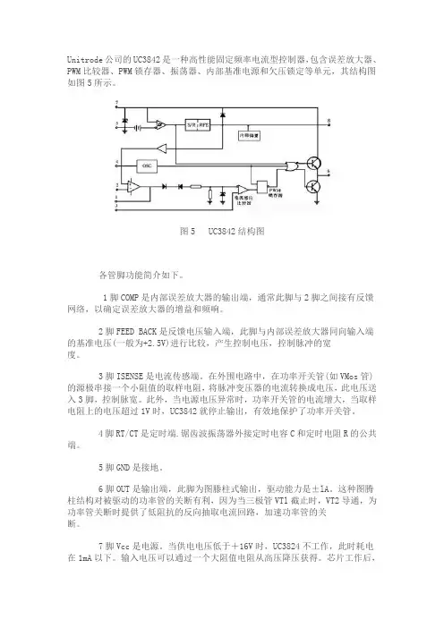
Unitrode公司的UC3842是一种高性能固定频率电流型控制器,包含误差放大器、PWM比较器、PWM锁存器、振荡器、内部基准电源和欠压锁定等单元,其结构图如图5所示。
图5 UC3842结构图各管脚功能简介如下。
1脚COMP是内部误差放大器的输出端,通常此脚与2脚之间接有反馈网络,以确定误差放大器的增益和频响。
2脚FEED BACK是反馈电压输入端,此脚与内部误差放大器同向输入端的基准电压(一般为+2.5V)进行比较,产生控制电压,控制脉冲的宽度。
3脚ISENSE是电流传感端。
在外围电路中,在功率开关管(如VMos管)的源极串接一个小阻值的取样电阻,将脉冲变压器的电流转换成电压,此电压送入3脚,控制脉宽。
此外,当电源电压异常时,功率开关管的电流增大,当取样电阻上的电压超过1V时,UC3842就停止输出,有效地保护了功率开关管。
4脚RT/CT是定时端.锯齿波振荡器外接定时电容C和定时电阻R的公共端。
5脚GND是接地。
6脚OUT是输出端,此脚为图滕柱式输出,驱动能力是±lA。
这种图腾柱结构对被驱动的功率管的关断有利,因为当三极管VTl截止时,VT2导通,为功率管关断时提供了低阻抗的反向抽取电流回路,加速功率管的关断。
7脚Vcc是电源。
当供电电压低于+16V时,UC3824不工作,此时耗电在1mA以下。
输入电压可以通过一个大阻值电阻从高压降压获得。
芯片工作后,输入电压可在+10~+30V之间波动,低于+10V停止工作。
工作时耗电约为15mA,此电流可通过反馈电阻提供。
8脚VREF是基准电压输出,可输出精确的+5V基准电压,电流可达50mA。
UV3842的电压调整率可达0.01%,工作频率为500kHz,启动电流小于1mA,输入电压为10~30V,基准电压为4.9~5.1V,工作温度为0~70℃,输出电流为1A。
开关稳压电源由UC3842A构成的开关电源电路如图6所示,T为高频变压器。
刚开机时,220V交流电先通过PNF滤掉射频干扰,再经过整流滤波获得约+300V直流电压,然后经R2降压后向UC3842提供+16V启动电压。
MULTILAYER CHIP CERAMIC CAPACITOR(:)DC Medium-voltage MLCCDC medium-voltage MLCC has good high-voltage reliability,it is made in special design that based on the MLCC technology and equipments.It is suitable for surface-mounting ,can improve the properties of circuits.New monolithic structureThe size of the capacitor is small,yet has high electrostatic capacitance,can operate at high-voltage levels.Has good solderability.Technology Parameter (refer to the picture below):DC-DC converter.The circuit filter and vibration bell of telephone,electrograph and modem.Snubber circuit for switching power supply.FeaturesApplicationsProduct Part Number Expression1206CG100J202NTWMULTILAYER CHIP CERAMIC CAPACITORCapacitance RangeOutside DimensionWMULTILAYER CHIP CERAMIC CAPACITORMULTILAYER CHIP CERAMIC CAPACITORMULTILAYER CHIP CERAMIC CAPACITOR【 南京南山半导体有限公司 — 贴片电容选型资料】MULTILAYER CHIP CERAMIC CAPACITORX7R 1808 (V)10018122225200 200 200 5001000 2000 3000 4000 100 500 1000 2000 3000 4000 100 500 1000 2000 3000 4000 5000 /250 /250 /250100PF 150PF 330PF 470PF 680PF 1000PF 1nF 2.2nF 3.3nF 4.7nF 6.8nF 10nF 12nF 15nF 22nF 27nF 33nF 39nF 47nF 56nF 68nF 100nF 120nF 150nF 220nF 270nF 330nF 470nF 680nF 1 F 2.2 F 3.3 F 10 F 22 F75【 南京南山半导体有限公司 — 贴片电容选型资料】ItemX7R Medium-voltage MLCCDielectric 1808 1812 2225 Size Rated 100 200 5001000 2000 3000 4000 100 200 500 1000 2000 3000 4000 100 200 500 1000 2000 3000 4000 5000 /250 /250 Volatage(V) /250 Capacitance 100PF 150PF 330PF 470PF 680PF 1000PF 1nF 2.2nF 3.3nF 4.7nF 6.8nF 10nF 12nF 15nF 22nF 27nF 33nF 39nF 47nF 56nF 68nF 100nF 120nF 150nF 220nF 270nF 330nF 470nF 680nF 1 F 2.2 F 3.3. F 10 F 22 F76【 南京南山半导体有限公司 — 贴片电容选型资料】MULTILAYER CHIP CERAMIC CAPACITORY5V 0603 (V) 100 100 0805 200 250 100 1206 200 250 100 1210 200 250 100 1812 200 250 100 2225 200 2501000PF 1.5nF 2.2nF 3.3nF 4.7nF 6.8nF 10nF 12nF 15nF 22nF 27nF 33nF 39nF 47nF 56nF 68nF 100nF 150nF 220nF 270nF 330nF 390nF 470nF 680nF 820nF 1 F 2.2 3.3 10 F F F77【 南京南山半导体有限公司 — 贴片电容选型资料】ItemY5V Medium-voltage MLCC 1210 100 200 250 100 1812 200 250 100 2225 200 250Dielectric 0603 0508 1206 Size Rated Volatage(V) 100 100 200 250 100 200 250 Capacitance 1000PF 1.5nF 2.2nF 3.3nF 4.7nF 6.8nF 10nF 12nF 15nF 22nF 27nF 33nF 39nF 47nF 56nF 68nF 100nF 150nF 220nF 270nF 330nF 390nF 470nF 680nF 820nF 1 2.2 3.3 10 F F F F78【 南京南山半导体有限公司 — 贴片电容选型资料】MULTILAYER CHIP CERAMIC CAPACITORCOG1-551251. 2. 3. 2 4. , , , , , 105.3 4 :HP4278A 1. 2. 5 (D.F.) 3. HP4284 25 5 :30% 75% 1.0 0.2V C<1000PF,1.0 0.1MHz; C 1000PF,1.0 0.1KHZ :10( :SF2511) >500V6I.R. 500V: , 60 5>1 5 7 >1 2 >1 21000V 1000V 2000V 2000V50mA 50mA 10mA 150+0/-10 60 55S 5S 5S824 2 -55 125 25975235 5 5 2 0.5 150+0/-10 5% 0.5PF, 10 1 D.F. 24 2 265 5 24 2 25 2.5mm/ : 25 2.5mm/ 60 524510I.R.1 2100 170120 2001 179【 南京南山半导体有限公司 — 贴片电容选型资料】Middle and high Voltage COG MLCC reliability test methodNumber 1 Item Operating Temperature Range Appearance -55 Standard 125 Test Method21.Good ceramic body color continuity. 2.The chips have no visual damages and must be very smooth. 3.No exposed innerelectrode, no cracks or holes. 4.The outer electrode should have no cracks, holes, damages or surface oxidation. 5.Outer electrode no prolongation or the prolongation is less than half of that of the termination width. Within the specified dimensions Within the specified toleranceCr 5PF 0.56% -4 5PF Cr 50PF 1.5[(150/Cr)+7] 10 Cr 50PF 0.15%Check by using microscope10.3 4Dimensions Capacitance Dissipation Factor (DF) Insulation ResistanceUsing micrometer or vernier calipers Measuring Equipment:HP4278 capacitance meter,HP4284 capacitance, Measuring Conditions: 1.Measuring Temperature:25 5 .Humidity: 30%~75%. 2.Measuring Voltage:1.0 0.2V. 3.Measuring Frequency:C<1000PF 1.0 0.1MHz C 1000PF 1.0 0.1KHz Measuring Equipment:Insulation resistance meter (such as Sf2511 insulation resistance). Measuring Method:Must measure at rated voltage, and if Ur>500V,then just use 500V,measure the IR within 60 1 seconds. Ur Max. Current Measuring Time 1000V 1000V 2000V 2000V 50mA 50mA 10mA 5S 5S 5S56C<10nF,IR 5 10 C>10nF,IR CR 500S10Withstanding Voltage 7Requirement >1.5Ur >1.2Ur >1.2Ur8Must meet the capacitor Capacitance temperature coefficient Temperature requirements within the Characteristics operating temperature range. Solderability Tin coverage 75% should be of the outer electrode covered by Tin Appearance Cap. Change ratio No defects visible 5% or 0.5PF whichever is bigger Same as original standard Same as original standardFirst, pre-heat: heat treat 60 5 minutes at 150+0/-10 , then set it for 24 2 hours at room temperature. Measure the capacitance at 55~125 or 55~85 , the capacitance change ratio comparing to that of 25 must be within the specified range. Dip the capacitor into ethanol or colophony solution, and then dip it into 235 5 eutectic solder solution for 2 0.5 seconds. Dipping speed: 25 2.5mm/second. First pre-heat: heat treat for 60 5 minutes at 150+0/-10 , then set it for 24 2 hours at room temperature. Then pre-heat the capacitance according to the following chart. Dip the capacitor into 265 5 eutectic solder solution for 10 1 seconds. Then set it for 24 2 hours at room temperature, then measure. Dipping speed: 25 2.5mm/second. Preheat conditions: Stage Temperature Time 1 2 100 170 120 200 1minutes 1minutes9 Resistance to Soldering10DFIR80【 南京南山半导体有限公司 — 贴片电容选型资料】MULTILAYER CHIP CERAMIC CAPACITOR1 10N11 10N,10 1 :1.0mm/ 11.5mm 10 D.F. 12 55Hz10 55Hz 10Hz 2 6 123 420 mmmm3mm mm mm mmmm150+0/-10 14 24 260 524 281【 南京南山半导体有限公司 — 贴片电容选型资料】NumberItem Adhesive Strength of TerminationStandard No removal of the termination or other defect shall occurTest Method Solder the capacitor to the test jig (glass epoxy resin board) shown in Fig.1 using a eutectic solder.Then apply a 10N force inthe direction shown as the arrowhead.The soldering shall be done either with an iron or using the reflow method and shall be conducted with care so that the soldering is uniform and free of defects such as heat shock,etc.11Fig.1 Vibration Resistance10N,10 1s Speed:1.0mm/s Glss epoxy resin board12Appearance No defects or Solder the capacitor to the test jig (glass epoxy resin abnormities board). The capacitor should be subjected to a simple harmonic motion having a total amplitude of 1.5mm, the Capacitance Within the frequency being varied uniformly between the specified approximate limits of 10 and 55Hz, shall be traversed tolerance range (from 10 Hz to 55 Hz then 10 Hz again) in approximately 1 minute.This motion shall be applied for a period of 2 DF Same as hours in each 3 mutually perpendicular directions original (total is 6 hours). standardFig.2 Bending Resistance No cracks or other defects shall occur Solder the capacitor to the test jig (glass epoxy resin board) shown in Fig.3 using a eutectic solder. Then apply a force in the direction shown in Fig.4. The soldering shall be done either with an iron or using the reflow method and shall be conducted with care so that the soldering is uniform and free of defects such as heat shock, etc. mmmm13mmmm mmmmTemperature Cycle 14Appearance No defects or abnormitiesPre-treatment: Heat-treat the capacitor for 60 5 minutes at 150+0/-10 , then set it for 24 2 hours at room temperature. Perform five cycles according to the four heat treatments listed in the following table. Set it for 24 2 hours at room temperature, the measure.82【 南京南山半导体有限公司 — 贴片电容选型资料】MULTILAYER CHIP CERAMIC CAPACITOR2.5% 0.25PF, min. 14 D.F. I.R. 10000M 1 2 3 4 2 3 30 2 30 2 3 3 3 34029095 24 2500+24/-05% 0.5PF, 15 ( ) D.F. I.R. 10000M1.5 50mA ( 5% 0.5PF, 16 .) >2000V100012 24 21.2D.F. I.R. 10000M83【 南京南山半导体有限公司 — 贴片电容选型资料】NumberItems Temperature CycleStandard Cap. Change ratio 2.5% or 0.25PF whichever is larger Same as original standard More than 10000M Heat-treatment:Test MethodD.F. 14 I.R.Stage Temperature Time 1 lowest operating temperature 3 30 2 2 Room Temperature 3 Highes operating temperature 2 30 4 Room Temperature 2min. 3 3 3 3Humidity Steady State 15AppearanceNo defects or abnormities 5% or 0.5PF whichever is larger Same as original standard More than 10000M No defects or abnormities 5% or 0.5PF (whichever is larger) Same as original standard More than 10000MSet the capacitor for 500+24/-0 hours at the condition of 40 2 and 90-95% humidity. Then remove and set it for 24 2 hours at room temperature, then measure.Cap. Change ratioD.F.I.R. Life Test AppearanceCap. Change ratio 16Apply 1.5 times rated voltage to the capacitor for 1000 12 hours at the upper temperature limits, the charging current should be less than 50mA. Remove and set it for 24 2 hours at room temperature, then measure.(If Ur>2000V,apply 1.2times Ur to test)D.F.I.R.84【 南京南山半导体有限公司 — 贴片电容选型资料】MULTILAYER CHIP CERAMIC CAPACITORX7R1-551251. 2. 3. 2 4. , , , , , 105.3 4 : HP4278A HP42845(D.F.)25010-41.255:30% 75% 2. 3. : :1.0 :1.0 0.2V 0.1KHz ( :SF2511 ) >500V , 60 56I.R.C 25nF,IR 10000M C>25nF,R C 500S 500V:>1 5 7 >1 2 >1 21000V 1000V 2000V 2000V50mA 50mA 10mA5S 5S 5S150+0/-10 24 8 25 -55 125 2605235 9 75 245 5 25 2.5mm/ 2 0.5585【 南京南山半导体有限公司 — 贴片电容选型资料】General X7R MLCC reliability test methodNumber 1 Item Operating Temperature Range Appearance -55 Standard 125 Test Method21.Good ceramic body color continuity. 2.The chips have no visualdamages and must be very smooth. 3.No exposed inner- electrode, no cracks or holes. 4.The outer electrode should have no cracks, holes, damages or surface oxidation. 5.Outer electrode no prolongation or the prolongation is less than half of the termination width. Within the specified dimensions Within the specified tolerance 250 10-4Check by using microscope10 .3 4Dimensions Capacitance Dissipation Factor (DF)5Using micrometer or vernier calipers Measuring Equipments: HP4278 capacitance meter, HP4284 capacitance, Measuring Conditions: 1.Measuring Temperature: 25 5 . Humidity: 30% 75%. 2.Measuring Voltage: 1.0 0.2V. 3.Measuring Frequency:1.0 0.1KHz Measuring Equipment: Insulation resistance meter (such as Sf2511 insulation resistance). Measuring Method: Must measure at rated voltage, and measure the IR within 60 1 seconds. Ur 1000V 1000V 2000V Max. Current Measuring Time 50mA 50mA 10mA 5S 5S 5SInsulation Resistance 6C 25nF,IR 10000M C>25nF,R C 500SWithstanding Voltage 7Requirement >1.5Ur >1.2Ur >1.2Ur2000V8Capacitance Temperature CharacteristicsMust meet the capacitor character temperature coefficient requirements within the operating temperature range. 75% of the outer electrode should be covered by TinFirst, pre-heat: heat treat 60 5 minutes at 150+0/-10 ,then set it for 24 2 hours at room temperature. Measure the capacitance at -55 125 ,the capacitance change ratio comparing to that of 25 must be within the specified range. Dip the capacitor into ethanol or colophony solution,and then dip it into 245 5 eutectic solder solution for 2 0.5 seconds. Dipping speed:25 2.5mm/second.Solderability 986【 南京南山半导体有限公司 — 贴片电容选型资料】MULTILAYER CHIP CERAMIC CAPACITOR150+0/-10 10% D.F. 10 I.R. 25 : 10 1 24 2 26560 5 24522.5mm/1 2100 170120 2001 1110N11 10N,10 1 :1.0mm/ 11.5mm 10 D.F. 55Hz 55Hz 10Hz 1 2 12 6 1023 13 ( ) 487【 南京南山半导体有限公司 — 贴片电容选型资料】NumberItemStandardTest Method First pre-heat: heat treat for 60 5 minutes at 150+0/-10 , then set it for 24 2 hours at room temperature. Then pre-heat the capacitance according to the following chart. Dip the capacitor into 265 5 eutectic solder solution for 10 1s. Then set it for 24 2 hours at room temperature, then measure. Dipping speed: 25 2.5mm/second. Preheat conditions: Stage Temperature Time 1 2 100 170 120 200 1minute 1minuteResistance to Appearance No defects visible Soldering Cap. Change Within 10% ratio DF 10 IR Same as original spec. Same as original spec.Adhesive Strength of TerminationNo removal of the terminations or other defect shall occur11Solder the capacitor to the test jig (glass epoxy resin board) shown in Fig.1 using a eutectic solder. Then apply a 10N force in the direction shown as the arrowhead. The soldering shall be done either with an iron or using the reflow method and shall be conducted with care so that the soldering is uniform and free of defects such as heat shock, etc. 10N,10 1s Speed:1.0mm/s Glss epoxy resinboardFig.1 Resistance to Soldering Appearance No defects visible or abnormities Capacitance Within the specified tolerance range D.F. 12 Same as original spec.Solder the capacitor to the test jig (glass epoxy resin board). The capacitor should be subjected to a simple harmonic motion having a total amplitude of 1.5mm, the frequency being varied uniformly between the approximate limits of 10 and 55Hz, shall be traversed (from 10 Hz to 55 Hz then 10 Hz again) in approximately 1 minute. This motion shall be applied for a period of 2 hours in each 3 mutually perpendicular directions (total is 6 hours).Fig.2 Bending Resistance No cracks or other defects shall occur Solder the capacitor to the test jig (glass epoxy resin board) shown in Fig.3 using a eutectic solder. Then apply a force in the direction shown as Fig.4. The soldering shall be done either with an iron or using the reflow method and shall be conducted with care so that the soldering is uniform and free of defects such as heat shock, etc.1388【 南京南山半导体有限公司 — 贴片电容选型资料】MULTILAYER CHIP CERAMIC CAPACITOR20 mmmmmm13mmmmmmmmmin. 20% 1 2 14 D.F. I.R. 3 4 2 3 30 2 30 2 3 3 3 340 20% 15 ( ) D.F. I.R.29095 48 2500+24/-01.5 20% .) 16 D.F. I.R 50mA ( >2000V100012 24 21.289【 南京南山半导体有限公司 — 贴片电容选型资料】NumberItem Bending ResistanceStandardTest Methodmmmmmm13mm mmmmTemperature CycleAppearanceNo defects or abnormities 20%Cap. Change Within ratio 14Stage Temperature Time min. 1 Min. Operating Temperature 3 30 3 2 Room Temperature 2 3 3 Max. Operating Temperature 2 30 3 4 Room Temperature 2 3D.F.Same as original Specification Same as original Specification No defects or abnormities 20% Set the capacitor for 500+24/-0 hours at the condition of 40 2 and 90-95% humidity. Then remove and set it for 48 2 hours at room temperature, then measure.I.R.Humidity Steady StateAppearanceCap. Change within ratio D.F.15 I.R. Life Test AppearanceSame as original Specification Same as original Specification No defects or abnonrmities 20% Apply 1.5 times rated voltage to the capacitor for 1000 12 hours at the upper temperature limits, the charging current should be less than 50mA. Remove and set it for 24 2 hours at room temperature, then measure.(If Ur>2000V,apply 1.2Ur to test.)Cap. Change within ratio 16 D.F.Same as original specification Same as original specificationI.R.90【 南京南山半导体有限公司 — 贴片电容选型资料】MULTILAYER CHIP CERAMIC CAPACITORY5V1-25~851. 2. 3. 2 4. 5. , , , , ,103 4 : HP4278A 1. 5 (D.F.) 500 10-4HP4284 25 5 75% 0.2V 0.1kHz:30% 2. 3. : :1.0 :1.06I.R.C 25nF,IR 40000M C>25nF,R C 500S( : ,: SF2511 60 5)7>300V >400V >500V100V 200V 250V50mA 50mA 50mA5S 5S 5S150+0/-10 8 24 -25 85 2605 25975235 25 0.52455 25 2.5mm/91【 南京南山半导体有限公司 — 贴片电容选型资料】General Y5V MLCC reliability test methodNumber 1 Item Operating Temperature Range Appearance -25 85 Standard Test Method21.Good ceramic body color continuity. 2.The chips have no visualdamages and must be very smooth. 3.No exposed inner- electrode, no cracks or holes. 4.The outer electrode should have no cracks, holes, damages or surface oxidation. 5.Outer electrode no prolongation or the prolongation is less than half of that of the termination width. Within the specified dimensions Within the specified tolerance 500 10-4Check by using microscope10.3 4Dimensions Capacitance) Dissipation Factor (DF)Using micrometer or vernier calipers Measuring Equipments: HP4278 capacitance meter, HP4284 capacitance, Measuring Conditions: 1.Measuring Temperature: 25 5 . Humidity: 30% 75%. 2.Measuring Voltage: 1.0 0.2V. 3.Measuring Frequency: 1.0 0.1KHz Measuring Equipment: Insulation resistance meter (such as Sf2511 insulation resistance). Measuring Method: Must measure at rated voltage, and measure the IR within 60 5seconds. Ur 1000V 1000V 2000V Max. Current Measuring Time 50mA 50mA 10mA 5S 5S 5S5Insulation Resistance 6C 25nF,IR 40000M C>25nF,R C 500SWithstanding Voltage 7Requirement >1.5Ur >1.2Ur >1.2Ur2000VCapacitance Temperature Characteristics 8Must meet the capacitor temperature coefficient requirements within the operating temperature range.First, pre-heat: heat treat 60 5 minutes at 150+0/-10 , then set it for 24 2 hours at room temperature. Measure the capacitance at 55 125 or 55 85 ,the capacitance change ratio comparing to that of 25 must be within the specified range. Dip the capacitor into ethanol or colophony solution,and then dip it into 235 5 (or 245 5 leadless eutectic solder solution) eutectic solder solution hanging lead for 2 0.5seconds. Dipping speed: 25 2.5mm/second.Solderability 975% of the outer electrode should be covered by Tin92【 南京南山半导体有限公司 — 贴片电容选型资料】MULTILAYER CHIP CERAMIC CAPACITOR150+0/-10 30% D.F. I.R. 10 60 5 24 22655 24 2 25 2.5mm/ :1011 2100 170120 200 11 110N11 10N,10 1 :1.0mm/ 11.5mm D.F. 10 55Hz 12 55Hz 10Hz 1 2 6 1023 ( 13 ) 493【 南京南山半导体有限公司 — 贴片电容选型资料】NumberItemStandardTest Method First pre-heat: heat treat for 60 5 minutes at 150+0/-10 , then set it for 24 2 hours at room temperature. Then pre-heat the capacitance according to the following chart. Dip the capacitor into 265 5 eutectic solder solution for 10 1s. Then set it for 24 2 hours at room temperature, then measure. Dipping speed: 25 2.5mm/second. Preheat conditions: Stage Temperature Time 1 2 100 170 120 200 1minute 1minuteResistance to Appearance No defects visible Soldering Cap. Change Z5U, Y5V: within ratio DF 10 IR30%Same as original spec. Same as original spec.Adhesive Strength of TerminationNo removal of the terminations or other defects shall occur11Solder the capacitor to the test jig (glass epoxy resin board) shown in Fig.1 using a eutectic solder. Then apply a 10N force in the direction shown as the arrowhead. The soldering shall be done either with an iron or using the reflow method and shall be conducted with care so that the soldering is uniform and free of defects such as heat shock, etc. 10N,10 1s Speed:1.0mm/s Glss epoxy resinboardFig.1 Resistance to Soldering Appearance No defects visible or abnormities Capacitance Within the specified tolerance range D.F. 12 Same as original spec.Solder the capacitor to the test jig (glass epoxy resin board). The capacitor should be subjected to a simple harmonic motion having a total amplitude of 1.5mm, the frequency being varied uniformly between the approximate limits of 10 and 55Hz, shall be traversed (from 10 Hz to 55 Hz then 10 Hz again) in approximately 1 minute. This motion shall be applied for a period of 2 hours in each 3 mutually perpendicular directions (total is 6 hours).Fig.2 Bending Resistance No cracks or other defects shall occur Solder the capacitor to the test jig (glass epoxy resin board) shown in Fig.3 using a eutectic solder. Then apply a force in the direction shown as Fig.4. The soldering shall be done either with an iron or using the reflow method and shall be conducted with care so that the soldering is uniform and free of defects such as heat shock, etc.1394【 南京南山半导体有限公司 — 贴片电容选型资料】MULTILAYER CHIP CERAMIC CAPACITOR20 mm mmmm13mm mmmmmm30%min. 1 2 3 4 3 2 30 2 30 2 3 3 3 3D.F. 14 I.R.40 30%29095 48 2500+24/-015()D.F. I.R.30% 16 D.F. I.R 48 21.5 50mA10001295【 南京南山半导体有限公司 — 贴片电容选型资料】NumberItem Bending ResistanceStandardTest Methodmmmm13mmmmmmmmTemperature CycleAppearanceNo defects or abnonrmities 2.5Cap. Change Within ratio 14Stage Temperature Time 30 1 Min. Operating Temperature 3 2 Room Temperature 2 3 Max. Operating Temperature 2 30 4 Room Temperature 2min. 3 3 3 3D.F.Same as original spec. Same as original spec. No defects or abnonrmities Set the capacitor for 500+24/-0 hours at the condition of 40 2 and 90-95% humidity. Then remove and set it for 24 2 hours at room temperature, then measure.I.R.Humidity Steady State 15AppearanceCap. Change within 30% ratio Same as D.F. original spec. I.R. Same as original spec. No defects or abnonrmities 30%Life TestAppearanceCap. Change within ratio 16 D.F.Same as original spec. Same as original spec.Apply 1.5 times rated voltage to the capacitor for 1000 12 hours at the upper temperature limits, the charging current should be less than 50mA. Remove and set it for 24 2 hours at room temperature, then measure.I.R.96。
课程设计任务书学生姓名:专业班级:指导教师:工作单位:信息工程学院题目:电容三端式振荡器(克拉泼振荡器)初始条件:计算机、Multisim软件要求完成的主要任务:(包括课程设计工作量及其技术要求,以及说明书撰写等具体要求)1、课程设计工作量:1周2、技术要求:(1)学习Multisim软件。
(2)正常工作状况时的波形图。
(3)起振条件的仿真,要求改变偏置电阻、相位电容和电源电压值,再观察起振波形和振荡电压的变化情况。
3、查阅至少5篇参考文献。
按《武汉理工大学课程设计工作规范》要求撰写设计报告书。
全文用A4纸打印,图纸应符合绘图规范。
时间安排:2014.9.18 下达任务书2014.9.19-9.26 根据要求设计电路,在计算机上仿真,并撰写课程设计报告书;2014年9月28日上午,鉴主13楼实验室答辩。
指导教师签名:年月日系主任(或责任教师)签名:年月日目录摘要 (I)Abstract (II)1绪论 (1)2绪论设计方案及原理 (1)2.1克拉泼振荡器简介 (2)2.2 设计方案 (2)2.3 设计原理 (4)2.4 参数计算 (5)3 Multisim仿真分析 (6)3.1 软件介绍 (6)3.2 克拉泼振荡器的仿真 (7)3.3 仿真结果分析 (11)4心得体会 (12)参考文献 (13)附录 (14)摘要克拉泼振荡器是电容三点式振荡器的改进型电路,属于LC振荡器的一种,它的振荡频率改变不影响反馈系数,振荡幅度比较稳定,广泛应用于各类电子设备中,克拉泼振荡器频率覆盖率较小,因此克拉泼振荡器适合作为固定频率的振荡器。
本文首先介绍了克拉泼振荡器的理论基础,紧接着计算了所设计电路的参数,从理论上论证了此电路的可行性,随后运用Multisim软件绘制了所设计的克拉泼振荡器并进行仿真,得到仿真结果,最后对仿真结果进行分析,并与理论值和理论波形进行比较。
关键词:克拉泼振荡器;Multisim;振荡频率;幅度AbstractCarat oscillator is the improved circuit of three-point capacitance oscillator, belongs to a kind of LC oscillator, the oscillation frequency changes will not affect the feedback coefficient of oscillation amplitude is stable, widely used in all kinds of electronic equipment, carat spilt oscillator frequency coverage is small, so the carat spilt oscillator for a fixed frequency oscillator.This article first introduces the theory foundation of carat spilt oscillator was followed by the calculation of the designed circuit parameters, theoretically demonstrates the feasibility of this circuit, and then use Multisim software made by carat spilt oscillator design and simulation, simulation results, finally the results of simulation is analyzed, and compared with the theoretical value and theoretical waveform.Keywords: Carat spilt oscillator;Multisim;Oscillation frequency;amplitude1绪论在电子线路中,除了要有对各种电信号进行放大的电子线路外,还需要有能在没有激励信号的情况下产生周期信号的电子电路,这种在无需外加激励信号的情况下,能将直流电能转换成具有一定波形、一定频率和一定幅度的交变能量的电子电路称为振荡器。
大学收音机实训报告(一)§1. 概述一、实训目的:1、学习收音机的装配与调试。
2、提高对整机电路图与电路板图的识读能力。
3、掌握收音机生产工艺流程,提高焊接与装配工艺水平。
4、通过收音机组装、调试、检修,使学生提高故障分析能力和动手能力,为更高端的家用电子产品维修打下坚实的理论和实践基础。
二、实训内容:1、HX218集成电路收音机电路原理分析。
2.收音机元器件识别与测量。
3.电路图与印制电路板的对应。
4.掌握印制电路板的组装及焊接工艺。
5.进行AM、FM中频、覆盖的调试及统调和整机测试。
6.收音机电路工作点的测量。
7.故障判断及排除。
三、实训基本要求:1、会识别、检测元器件并判别其质量。
2、能独立识读电路图和印制板图并完成各测试点的测量与整机安装。
3、会排除在调试与装配过程中可能出现的问题与故障。
4、所制作的产品电器性能指标应能满足三级机水平(国标),具体如下:①接收频率范围:AM 535~1605KHZ FM 87~108MHZ②接收灵敏度:AM 达国家C类标准FM 优于μV级③输出功率大于100mW ④供电电源: DC 3V§2. 收音机的基本工作原理1、收音机的电路结构种类有很多,早期生产的收音机多为分立元件电路,目前基本上都采用了大规模集成电路为核心的电路(本机电路采用日本索尼公司生产的调频调幅专用集成电路CXA1691M,国产型号为CD1691M)。
集成电路收音机的特点是:结构比较简单,性能指标优越,体积小等优点。
AM/FM型的收音机电路可用如图1所示的方框图来表示。
收音机通过调谐回路选出所需的电台,送到变频器与本机振荡电路送出的本振信号进行混频,然后选出差频作为中频输出(我国规定的AM中频为465KHZ,FM中频为10.7MHZ),中频信号经过检波器检波后输出调制信号(低频信号),调制信号(低频信号)经低频放大、功率放大后获得足够的电流和电压,即功率,再推动喇叭发出响亮的声音。
三端稳压器国内外各厂家生产的三端(电压输入端,电压输出端,公共接地端)固定式正压稳压器均命名为78系列,该系列稳压器有过流,过热和调整管安全工作区保护,以防止过载而损坏。
其中78后面的数字代表稳压器输出的正电压数值(一般有05V,06V,08V,09V,10V,12V,15V,18V,24V共9种输出电压),各厂家在78前面冠以不同的英文字母代号。
78系列稳压器最大输出电流分100mA,500mA,1.5A三种,已插入78和电压数字之间的字母表示。
插入L表示100mA,M表示500mA,如不插入字母则表示1.5A。
此外,78(L,M)XX的后面往往还附有表示输出电压容差和封装外壳类型的字母。
常见的封装形式有TO-3金属和TO-220的塑料封装。
TO-3金属封装形式输出电流可以达到5A。
三端稳压电路注意事项在实际应用中,应在三端集成稳压电路上安装足够大的散热器(当然小功率的条件下不用)。
当稳压管温度过高时,稳压性能将变差,甚至损坏。
当制作中需要一个能输出1.5A以上电流的稳压电源,通常采用几块三端稳压电路并联起来,使其最大输出电流为N个1.5A,但应用时需注意:并联使用的集成稳压电路应采用同一厂家、同一批号的产品,以保证参数的一致。
另外在输出电流上留有一定的余量,以避免个别集成稳压电路失效时导致其他电路的连锁烧毁。
在78 ** 、79 ** 系列三端稳压器中最常应用的是TO-220和TO-202两种封装。
这两种封装的图形以及脚序号、引脚功能如附图所示。
从正面看①②③引脚从左向右按顺序标注,接入电路时①脚电压高于②脚,③脚为输出位。
如对于78**正压系列,①脚高电位,②脚接地,;对与79**负压系列,①脚接地,②脚接负电压,输出都是③脚。
如附图所示。
此外,还应注意,散热片总是和接地脚相连。
这样在78**系列中,散热片和②脚连接,而在79**系列中,散热片却和①脚连接。
三端固定式正压稳压器三端固定式稳压器的基本应用电路如图3.1.4所示,只要把正输入电压Ui加到MC7805的输入端,MC7805的公共端接地,其输出端便能输出芯片标称正电压Uo。
Disc-Type EMIFIL® (A miniature three-terminal capacitor)DSS6N □□□□□□□□□□□ Reference Specification1.ScopeThis reference specification applies to DSS6N series.2.Part Numbering(Ex.) DS S 6 N B3 2A 271 Q93 A ① ② ③ ④ ⑤ ⑥ ⑦ ⑧ ⑨① Product ID (Disc-Type EMIFIL®)② Structure S : Built-in Ferrite Beads Type ③ Style ④ Features⑤ Temperature Characteristics ⑥ Rated Voltage⑦ Capacitance□□□Marked three digits system.(Ex. 270pF →271)⑧ Lead TypeQ5□/ T □1 : Bulk (in mm) Q9□/ U □1 : Taping (in mm) Straight Lead Type Q91 Q92 Q93 Incrimp Lead Type - U21 U31Dimension H 20.0±1.0 16.5±1.0 18.5±1.0 Dimension H : See item 9.⑨ Packaging Code A : Ammo Pack / B : Bulk3.RatingOperating temperature : -25 to +85°CStorage Temperature : -25 to +85°C Insulation Resistance : 5000M Ω min. (DSS6NB3 / DSS6NE3 /DSS6NZ8) Rated Current : 6A(DC) Equivalent Circuit :Others : See Table 1Table 1CustomerPart NumberMurata Part Number Temperature CharacteristicsCapacitanceRated VoltageWithstanding Voltage Unit Mass (Typical value)DSS6NB32A220Q55B ±10% 22pF± 20%100V(DC)250 V(DC)0.43g DSS6NB32A220Q56B 0.43g DSS6NB32A220Q54B 0.43g DSS6NB32A220T51B 0.47g DSS6NB32A220T41B 0.47gDSS6NB32A220Q91A 0.43g DSS6NB32A220Q92A 0.43g DSS6NB32A220Q93A 0.43g DSS6NB32A220U21A 0.43gDSS6NB32A220U31A0.43gGND 1(3)3(1)2Customer Part NumberMurataPart NumberTemperatureCharacteristics CapacitanceRatedVoltageWithstandingVoltageUnit Mass(Typical value) DSS6NB32A330Q55B±10%33pF± 20%100V(DC)250 V(DC)0.43g DSS6NB32A330Q56B 0.43g DSS6NB32A330Q54B 0.43g DSS6NB32A330T51B 0.47g DSS6NB32A330T41B 0.47g DSS6NB32A330Q91A 0.43g DSS6NB32A330Q92A 0.43g DSS6NB32A330Q93A 0.43g DSS6NB32A330U21A 0.43g DSS6NB32A330U31A 0.43g DSS6NB32A470Q55B47pF± 20%0.42g DSS6NB32A470Q56B 0.42g DSS6NB32A470Q54B 0.42g DSS6NB32A470T51B 0.46g DSS6NB32A470T41B 0.46g DSS6NB32A470Q91A 0.42g DSS6NB32A470Q92A 0.42g DSS6NB32A470Q93A 0.42g DSS6NB32A470U21A 0.42g DSS6NB32A470U31A 0.42g DSS6NB32A101Q55B100pF±20%0.42g DSS6NB32A101Q56B 0.42g DSS6NB32A101Q54B 0.42g DSS6NB32A101T51B 0.46g DSS6NB32A101T41B 0.46g DSS6NB32A101Q91A 0.42g DSS6NB32A101Q92A 0.42g DSS6NB32A101Q93A 0.42g DSS6NB32A101U21A 0.42g DSS6NB32A101U31A 0.42g DSS6NB32A151Q55B150pF±20%0.42g DSS6NB32A151Q56B 0.42g DSS6NB32A151Q54B 0.42g DSS6NB32A151T51B 0.46g DSS6NB32A151T41B 0.46g DSS6NB32A151Q91A 0.42g DSS6NB32A151Q92A 0.42g DSS6NB32A151Q93A 0.42g DSS6NB32A151U21A 0.42g DSS6NB32A151U31A 0.42gDSS6NB32A221Q55B220pF±20% 0.42gDSS6NB32A221Q56B 0.42g DSS6NB32A221Q54B 0.42g DSS6NB32A221T51B 0.46g DSS6NB32A221T41B 0.46g DSS6NB32A221Q91A 0.42g DSS6NB32A221Q92A 0.42g DSS6NB32A221Q93A 0.42g DSS6NB32A221U21A 0.42g DSS6NB32A221U31A 0.42gCustomer Part NumberMurataPart NumberTemperatureCharacteristics CapacitanceRatedVoltageWithstandingVoltageUnit Mass(Typical value) DSS6NB32A271Q55B±10%270pF±20%100V(DC)250 V(DC)0.42gDSS6NB32A271Q56B 0.42g DSS6NB32A271Q54B 0.42g DSS6NB32A271T51B 0.46g DSS6NB32A271T41B 0.46g DSS6NB32A271Q91A 0.42g DSS6NB32A271Q92A 0.42g DSS6NB32A271Q93A 0.42g DSS6NB32A271U21A 0.42g DSS6NB32A271U31A 0.42gDSS6NB32A471Q55B470pF±20% 0.43gDSS6NB32A471Q56B 0.43g DSS6NB32A471Q54B 0.43g DSS6NB32A471T51B 0.47g DSS6NB32A471T41B 0.47g DSS6NB32A471Q91A 0.43g DSS6NB32A471Q92A 0.43g DSS6NB32A471Q93A 0.43g DSS6NB32A471U21A 0.43g DSS6NB32A471U31A 0.43gDSS6NB32A102Q55B1000pF±20% 0.42gDSS6NB32A102Q56B 0.42g DSS6NB32A102Q54B 0.42g DSS6NB32A102T51B 0.46g DSS6NB32A102T41B 0.46g DSS6NB32A102Q91A 0.42g DSS6NB32A102Q92A 0.42g DSS6NB32A102Q93A 0.42g DSS6NB32A102U21A 0.42g DSS6NB32A102U31A 0.42g DSS6NE32A222Q55B± 2055 %2200pF±8020%0.42gDSS6NE32A222Q56B 0.42g DSS6NE32A222Q54B 0.42g DSS6NE32A222T51B 0.46g DSS6NE32A222T41B 0.46g DSS6NE32A222Q91A 0.42g DSS6NE32A222Q92A 0.42g DSS6NE32A222Q93A 0.42g DSS6NE32A222U21A 0.42g DSS6NE32A222U31A 0.42g DSS6NZ82A103Q55B± 3085%10000pF±30 %0.42gDSS6NZ82A103Q56B 0.42g DSS6NZ82A103Q54B 0.42g DSS6NZ82A103T51B 0.46g DSS6NZ82A103T41B 0.46g DSS6NZ82A103Q91A 0.42g DSS6NZ82A103Q92A 0.42g DSS6NZ82A103Q93A 0.42g DSS6NZ82A103U21A 0.42g DSS6NZ82A103U31A 0.42g4.Testing Conditions<Unless otherwise specified> <In case of doubt> Temperature : Ordinary Temperature 15 to 35°C Temperature: 20 ± 2°CHumidity : Ordinary Humidity 25 to 85 %(RH) Humidity : 60 to 70 %(RH)Atmospheric Pressure : 86 to 106 kPa 5.Style and DimensionSee item 9.6.Marking7.PerformanceNo. Item Specification TestMethod7.1 AppearanceandDimensions Meet item 9. Visual Inspection and measured with SlideCalipers.7.2 Marking Marking is able to be read easily. Visual Inspection.7.3 CapacitanceandToleranceMeet item 3. Table 27.4 InsulationResistance(I.R.) Meet item 3. Test Voltage : Rated VoltageTime : 1 minute through a suitable resistor 1MΩ.7.5 WithstandingVoltage Products shall not be damaged. Test Voltage : 2.5 times for Rated VoltageTime : 1 to 5 secondsCharge Current : 10 mA max.It shall be applied between input / output terminaland ground terminal.7.6 TemperatureCharacteristics Meet item 3. Capacitance shall be measured at each stepspecified in Table 3 after reaching the thermalequilibrium.The capacitance change against the capacitanceat step 3 shall be calculated.( ) is for DSS6NZ82A103.Table37.7 Solderability Along the circumference of terminalshall be covered with new solder atleast 75%. Flux : Ethanol solution of rosin,25(wt)%(dipped for 5 to 10 seconds)Pre-heat : 150±10℃, 60~90 sSolder : Sn-3.0Ag-0.5CuSolder Temperature 245±5℃Immersion Time : 2 ± 0.5 secondsImmersion Depth :2 to 2.5 mm from the bottom of the body. Frequency TestVoltage Capacitance1±0.1MHz 3 V(rms) max. 22pF~100pF1±0.1kHz 3 V(rms) max. 150pF~10000pFStep 1 2 3 4 5 Temp.(°C)+20±2-25±2(-10)+20±2 +85±2(60)+20±2No. Item Specification TestMethod7.8 ResistancetoSoldering Heat Meet Table 4.Table 4Flux : Ethanol solution of rosin,25(wt)%(dipped for 5 to 10 seconds)Pre-heat : 150±10℃, 60~90 sSolder : Sn-3.0Ag-0.5CuSolder Temperature : 270 ± 5 °CImmersion Time : 3± 0.5 secondsImmersion Depth :1.6 ± 0.7 mm from the bottom of the body.Then measured after exposure in the roomcondition for 4 to 24hours.Appearance Nodamaged.CapacitanceChangeB3 within ± 5%E3 within ± 15%Z8 within ± 20%WithstandingVoltageNo damaged.7.9 Humidity MeetTable5.Table 5 Temperature : 40 ± 2°CHumidity : 90 to 95 %(RH)Time : 500 hours(+24-0 hours)Then measured after exposure in the room condition for 4 to 24hours.Appearance Nodamaged.Capacitance Change B3 within ± 10% E3, within ± 20% Z8 within ± 30%Insulation Resistance B3,E3Z81000MΩ min.7.10 Humidity Life Meet Table6.Table 6 Temperature : 40 ± 2°CHumidity : 90 to 95 %(RH)Time : 500 hours(+24-0 hours)Applying Voltage : Rated VoltageCharge Current : 10 mA max.Then measured after exposure in the room condition for 4 to 24hours.7.11 Heat Life Meet Table 7.Table 7 Temperature : 85 ± 3°CTime : 1000 hours(+48-0 hours)Applying Voltage :B3,E3 character : 2 times of DC rated voltage Z8character : 1.5times of DC rated voltage Charge Current : 10 mA max.Then measured after exposure in the room condition for 4 to 24hours.Appearance No damaged.Capacitance Change B3 within ± 10% E3 within ± 20% Z8 within ± 30%Insulation Resistance B3,E3Z8500MΩ min.Appearance Nodamaged.Capacitance Change B3 within ± 10% E3 within ± 20% Z8 within ± 30%Insulation Resistance B3,E3Z8 1000MΩ min.8.Mounting HoleBulk Taping9.Style and Dimension(1) Bulk(Straight Lead Type) : Q5□*1.Bottom of dielectric may be exposed. *2.There should not be the exposureof the ferrite bead if a hole is on the top of ferrite bead.(in mm)(2) Bulk (Incrimp Lead Type) : T □1*1.Bottom of dielectric may be exposed. *2.There should not be the exposure of the ferrite bead if a hole is on the top of ferrite bead.(in mm)(3) Taping(Straight Lead Type) : Q9□(All symbols in the illustrations below are described in Table 8)(in mm)*1.Bottom of dielectric may be exposed.*2.There should not be the exposure of the ferrite bead if a hole is on the top of ferrite bead.Lead Type l Q55 25.0 min. Q56 6.0±1.0 Q544.0±0.5 in m m Lead Type l T51 25.0 min. T41 4.0±0.5 8.0max.*1φ0.6F15.0±0.5F1lF1=2.5±0.5M arking side Marking side2.54m ax.*27.0m a x .1 2 3(3) (1) 8.0m ax.*1φ0.6F15.0±0.5F110.0m a x .lF1=2.5±0.5M arking sideMarking side2.54m ax.1.0±0.2Detail of form ing*21 2 3(3) (1)t 2t 1(4) Taping (Incrimp Lead Type) : U □1*1.Bottom of dielectric may be exposed.*2.There should not be the exposure of the ferrite bead if a hole is on the top of ferrite bead. Table 8Code Description DimensionsRemarkP Pitch of Component12.7 Product Inclination∆S Determines Crossing P 0 Pitch of Sprocket Hole12.7±0.2 P 1Length from Hole Center to Lead 3.75±0.7P 2Length from Hole Centerto Component Center 6.35±1.3Shift In TapeIn Direction of Feed D Width of Body7.0 max.∆SDeviation along tape, Left or Right 0±1.0W Carrier Tape Width 17.0±0.5W 1 Position of Sprocket Hole 9.0+0,-0.5 Tape Widthwise Shift l Protrusion Length +0.5 ~ -1.0 D 0 Diameter of Sprocket Hole φ4.0±0.1 d Lead Diameter φ 0.6t 1 Total Tape Thickness 0.7±0.2 Includes Thickness of Bonding Tapet 2 Total Thickness,Tape and Lead Wire 1.5 max. ∆h 1 Deviation across Tape,front 1.0 max.∆h 2 Deviation across Tape,rear 1.0 max. L Portion to Cut in Case of Defect 11.0+0,-1.0 W 0 Hold Down Tape Width 12.0±0.5 W 2 Hold Down Tape Position1.5±1.5H Lead length between sprocket hole and forming positionQ91 20.0±1.0 Q92U2116.5±1.0 Q93U3118.5±1.0F Lead Spacing 5.0+0.7,-0.2F 1 2.5+0.4,-0.2(in mm)t 2t 110.Taping10.1 Supplement condition of taping(1) A maximum of 0.3% of the components quantity per reel or Ammo pack may be missing without consecutive missing components.(2) The adhesive power of the tape shall have over 2.94N at the following condition.(3) Splicing method of tape1. Carrier tapeCarrier tape shall be spliced by cellophane tape. Overall thickness shall be less than 1.05 mm.(in mm)2. Hold down tapeHold down tape shall be spliced with overlapping. Overall thickness shall be less than 1.05 mm.(in mm)3. Both carrier tape and hold down tapeBoth tapes shall be cut zigzag and spliced with splicing tape.11. Packing11.1 Packing quantityThe standard packing quantity is as follows.(The packing quantity may be changed due to a fraction of order.)Minimum Packing Form and QuantityTerminal Configuration A Unit Quantity Bulk : in a plastic bag Taping : in an ammo pack * Standard Quantityin a container(corrugated cardboard box)BulkLong Lead Type (Q55/T51) 250 pcs. 5000 pcs.Short Lead Type (Q54/Q56/T41)500 pcs.10000 pcs.Taping (Q91/ Q92/ Q93/U21/U31) 2000 pcs.20000 pcs.* A quantity in a container is depending on a quantity of an order.11.2 Packing Form(1) Bulk<A plastic bag pack>1.Products are packed into a plastic bag.2.The plastic bags are put into a container(corrugated cardboard box) depending on aquantity of an order.F 2.94N Direction of feed Direction of feeda plastic bagcontainer labela containerthe plastic bag with products(2) Taping<An ammo pack>1 .Folding the tape per 25 pitches,products are packed into an ammo package so that each product of each layer wound zigzag is put on top of one another. [Fig 1]2. The dimensions of the ammo package are indicated in [Fig 2].3. The ammo packages are put into a container (corrugated cardboard box) depending on a quantity of an order.4. Not less than 3 consecutive of component shall be missing on both edge of tape.[Fig 1] [Fig 2]The unloading direction : RightThe hold down tape : Upper (in mm) The product body : Left along the unloading direction12.Marking on package12.1 Unit PackageBulk : Marked on a plastic bag.Taping : Marked on a label stuck on an ammo package.Marking on a unit package consists of :Customer part number , MURATA part number, Inspection number(*1), RoHS marking (*2), Quantity, etc*1) « Expression of Inspection No. » □□ OOOO ⨯⨯⨯(1) (2) (3)(1) Factory Code(2) Date First digit : Year / Last digit of year Second digit : Month / Jan. to Sep. → 1 to 9, Oct. to Dec. → O,N,DThird, Fourth digit : Day(3) Serial No.*2) « Expression of RoHS marking »ROHS – Y (△)(1) (2)(1) RoHS regulation conformity parts. (2) MURATA classification number12.2 ContainerMarking on the label stuck on a container consists of :Customer name Purchasing Order Number, Customer Part Number, MURATA part number, RoHS marking (*2), Quantity, etc13.△!Caution13.1 Mounting holesMounting holes should be designed as specified in this specifications.Or different design from this specifications may cause cracks in ceramics which may lead to smoking / firing.13.2 Caution for the product angle adjust workTake care not to apply any mechanical stress to product body at the lead terminal bending process for productangle adjustment after insertion.13.3 Limitation of ApplicationsPlease contact us before using our products for the applications listed below which require especially high reliability for the prevention of defects which might directly cause damage to the third party's life, body or property. (1) Aircraft equipment (7) Traffic signal equipment (2) Aerospace equipment (7) Disaster prevention / crime prevention equipment (3) Undersea equipment (9) Data-processing equipment(4) Power plant control equipment (10) Applications of similar complexity and /or reliability requirements (5) Medical equipment to the applications listed in the above (6) Transportation equipment (vehicles, trains, ships, etc.)zigzag label340max.240m ax.51m ax.14. Notice14.1 Soldering(1) Use rosin-based flux. Do not use strong acidic flux with halide content exceeding 0.2(wt)% (chlorine conversion value). Use Sn-3.0Ag-0.5Cu solder(2) Standard flow soldering profile.Solder temperature Soldering time 250~260 °C 4~6s(3) Resistance to soldering iron goes in the following condition that tip temperature is 350 °C max. andsoldering time is 5 s max.(4) Products and the leads should not be subjected to any mechanical stress during soldering process.(and also while subjected to the equivalent high temperature.)14.2 CleaningProducts shall be cleaned on following conditions.(1) Cleaning Temperature: 60℃ max.(40℃ max. for Isopropyl alcohol).(2) Ultrasonic cleaning shall comply with the following conditions, avoiding the resonance phenomenon at the mounted products and P .C.B.Power :20W / l max.Frequency :28kHz 40kHz Time :5 minutes max.(3) Cleaning agent1. alcohol cleaning agents.・Isopropyl alcohol (IPA)2. Aqueous cleaning agent・Pine Alpha ST-100S(4) Ensure that residual flux and residual cleaning agent is completely removed.Products should be thoroughly dried after aqueous agent has been removed with de-ionized water. (5) For other cleaning methods, please contact Murata engineering.14.3 Operating Environment(1) Do not use products in corrosive gases such as chlorine gas, acid or sulfide gas.(2) Do not use products in the environment where water, oil or organic solvents may adhere to products.(3) Do not adhere any resin to products, coat nor mold products with any resin (including adhesive)to preventmechanical and chemical stress on products.14.4.Storage and handling requirements.(1) Storage periodUse the products within 12 months after delivered.Solderability should be checked if this period is exceeded. (2) Storage environment conditionTo prevent products quality deterioration, stored conditions should be controlled as follows ; 1. Temperature : -10 to 40 degrees centigrade 2. Humidity : 15 to 85% relative humidity3. Products should be stored without sudden changes in temperature and humidity. Don't keep products in corrosive gases such as sulfur,chlorine gas or acid, or it may cause oxidization of lead terminals resulting in poor solderability.4. Products should be stored on the palette for the prevention of the influence from humidity, dust and so on.5. Products should be stored in the warehouse without heat shock, vibration,direct sunlight and so on. (3) Handling ConditionsCare should be taken when transporting or handling product to avoid excessive vibration or mechanical shock.1minutes min.Soldering tim eSolder tem p.25020015010050T e m p e r a t u r e (°C )Pre -heating(in air)Soldering Gradual Cooling(in air)300Spec No. JENF243F-0018K-01 P11/11 MURATA MFG.CO., LTD Reference Only 15. △!Note (1)Please make sure that your product has been evaluated in view of your specifications with our product being mounted to your product.(2)You are requested not to use our product deviating from the reference specifications.(3)The contents of this reference specification are subject to change without advance notice. Please approve our product specifications or transact the approval sheet for product specifications before ordering.。
swsx vusy vuvs vwswvwvu!" 7 4# $8 %8 $4! 884%48 7&$345365)*+,-./+01,2,1*),3-)4564789:;58588<=>?@:98>?:AB *C +;589);5=>?B DC 14789:;58588<=>?E=986:=4>?E=986:=4>?E =986:=4>!" 7 4# $8 %8 $4! 884%48 7&$gg54>8>:@54>8>:@+986;G:=4>@a49:A8G@84a?8>89;<p Z11!" 7 4# $8 %8 $4! 884%48 7&$%8%8!" 7 4# $8 %8 $4! 884%48 7&$|6!" 7 4# $8 %8 $4! 884%48 7&$!" 7 4# $8 %8 $4! 884%48 7&$/:;?8@+986;G:=4>@)86A>=6;<64>@=E89;:=4>@VM /4<E89=>?PMX A8>:44J G6A A;<4?8>;:8E @GD@:;>68B 1A<49=>8l8:6C64>:8>:=@G@8E :4;6:=7;:8:A8a <G_l49A=?A<I ;6=E=6a <G_=@G@8El;>8_68@@=78;J 4G>:4a 98@=EG8;a :89@4<E89=>?J ;I <8;E :464994@=4>4a:A8:89J =>;<8<86:94E8@49E8?9;E;:=4>4a=>@G<;:=4>98@=@:;>684>:A8@G9a ;684a:A86;5;6=:49@M QM 2<G_=@G@8E :4=>698;@8@4<E89;D=<=:I =>a <4b @4<E89=>?lDG:=a:44J G6Aa <G_=@;55<=8El;<;9?8;J 4G>:4aa <G_?;@J ;I D88J =::8E ;>E J ;I E8:9=J 8>:;<<I ;a a 86:@4<E89;D=<=:I M)4J =>=J =^8:A8;J 4G>:4aa <G_;55<=8El =:=@9864J J 8>E8E :4G@8;a <G_U DGDD<=>?@I@:8J M[M /=>68:A898@=EG84ab ;:89U @4<GD<8a <G_=@8;@=<I E=@@4<78E DI b ;:8964>:8>:=>:A8;=9l:A898@=EG84>:A8@G9a ;684a6;5;6=:49@=>A=?A AGJ =E=:I 64>E=:=4>@J ;I 6;G@8;E8?9;E;:=4>4a=>@G<;:=4>98@=@:;>68;>E :A898a 498;a a 86::A898<=;D=<=:I 4a:A864J 54>8>:@M)A86<8;>=>?J 8:A4E@;>E :A86;5;D=<=:I 4a:A8J ;6A=>8@G@8E @A4G<E ;<@4D864>@=E898E 6;98a G<<I b A8>@8<86:=>?b ;:89U @4<GD<8a <G_M +98A8;:=>?b A8>@4<E89=>?Y 8;:=>?k+98A8;::A86A=5@;:POO:4P[O POO D8a 498@4<E89=>?M144<=>?k)A8:8J 589;:G98E=a a 898>68D8:b 88>:A864J 54>8>:@;>E 6<8;>=>?59468@@@A4G<E >4:D8?98;:89:A;>POO M189;J =66A=56;5;6=:49@;98@G@685:=D<8:4:A89J ;<@A46H b A8>8_54@8E :49;5=E 4964>68>:9;:8E A8;:=>?499;5=E 644<=>?l)A898a 498l:A8@4<E89=>?59468@@J G@:D864>EG6:8E b =:A ?98;:6;98@4;@:459878>:J ;<a G>6:=4>4a:A864J 54>8>:@EG8:48_68@@=78:A89J ;<@A46HM¡¢£¡¢£¡¢£¡¢£¡¢£¡¢£¤¥¤¦¤§¤¨¤¨¤©¤ª¤¢©¨¤¥©¨©¤««««««««««««««««««2222«2222T 2222««««¬ «¬ «¬ «¬«¬ «¬ «¬ «¬ «¬m864>J J 8>E8E /4<E89=>?p 8:A4E®¯°±²³´µ¶±·¸®°±¹¯®º®¯±²³´µ¬¬»¼±®¯°±²³´µ³½±¾±¶¿±²»·À²± »·±°£®¯·»µ±Á»¿»Â³·»´Â±®¯°±²³´µÁ¸»²»Â·±²³Ã·³ÂÃı·¸®°35!" 7 4# $8 %8 $4! 884%48 7&$3!" 7 4# $8 %8 $4! 884%48 7&$35%86%86h Í!" 7 4# $8 %8 $4! 884%48 7&$Stages Precautions Technical considerations8.Storage Condition s Storage1.To maintain the solderability of terminalelectrodes and to keep the packagingmaterial in good condition,care must betaken to control temperature and humidityin the storage area.Humidity shouldespecially be kept as low as possible.Recommended conditionsTemperature040Humidity Below70%RHThe room temperature must below40.Even under ideal storage conditions capacitor electrode solderability decreased as time passes,so ceramic chip capacitors should be used within6months from the time of delivery.The packaging material should be kept where nochlorine or sulfur exist in the air.2.The capacitance value of high dielectric constant capacitors(type2&3)will gradually decrease with thePassage of time,so this should be taken into consideration in the circuit design.If such a capacitance reduction occurs,a heat treatment of150for1hour will return the capacitance to its initial level.1.If the parts are stored in a high temperatureand humidity environment,problems such asreduced solderability caused by oxidation ofterminal electrodes and deterioration oftaping/packaging materials may take place.Forthis reason,components should be used within6months from the rime of delivery.If exceedingthe above period,please check solderabilitybefore using the capacitors.6.Post cleaning Processes With some type of resins a decomposition gas or chemical reaction vapor may remain inside the resin during the hardening period or even while left under normal storage conditionswill result in the deterioration of thecapacitor s ps hs o。