MEMS 课件 litho&etching
- 格式:pdf
- 大小:1.41 MB
- 文档页数:41

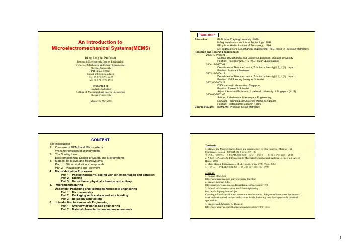
Inertia Sensor for Automobile “Air Bag”Micro inertia sensor (accelerometer) in place:Sensor-on-a-chip:(2 mm x 3 mm-smaller thanrice grain(Courtesy of Analog Devices, Inc)Rice grainsOver 100 micro-sensors and micro-actuators by MEMS technologyThe ENIAC Computer in 1946A “Palm-top”Computer in 2003This spectacular miniaturization took place in 50 years!!The ENIAC computerMobil phones 15 Years Ago:Current State-of-the Art:Transceive voice onlyTransceive voice+ others Palm-top Wireless PCThe only solution is to pack manyMicro pressure sensorsInertia Sensor for Automobile “Air Bag”Micro inertia sensor (accelerometer) in place:Sensor-on-a-chip:(the size of arice grain(Courtesy of Analog Devices, Inc) Unique Features of MEMS and Microsystems (1)-A great challenge to engineersComponents are in micrometers with complex geometryusing silicon, si-compounds and polymers:25 µmA microgear-train by(1)(10)(2)(3)(4)(5)(6)(8)(9)(2) Exhaust gas differential pressure sensor(1) Manifold or Temperature manifold absolute pressure sensor (3) Fuel rail pressure sensor(4) Barometric absolute pressure sensor (5) Combustion sensor(7) Fuel tank evaporative fuel pressure sensor (6) Gasoline direct injection pressure sensor (8) Engine oil sensor (9) Transmission sensor (10) Tire pressure sensorApplication of MEMS and MicrosystemsinAerospace IndustryCockpit instrumentation.Wind tunnel instrumentation MicrosattellitesCommand and control systems with MEMtronicsInertial guidance systems with microgyroscopes, accelerometers and fiber optic gyroscope.Attitude determination and control systems with micro sun and Earth sensors.Power systems with MEMtronic switches for active solar cell array reconfiguration, andMicro lenses:Micro switches: Micro Optical SwitchesMigratingElectrons The strains associated with the deformation of the diaphragm areplaced in “strategic locations”onThese tiny piezoresistors are madeThere is preset mismatch of pitches of the electrodes in the two sets.Stator RotorGear fortransmittingtorqueStationary electrodesMoving electrodeThe movement of the proof mass is carried out by measuring the change of capacitances between the pairs of electrodes.B e a m M ov e m e n tA c ce l e r a t i o nThe need for integrating microelectronics (ICs)and moving microstructures –A great challenge!A c c e l e r a t i o n3 mm2 mm。



EE C245: Introduction to MEMS DesignLecM 4C. Nguyen8/20/091EE C245 –ME C218Introduction to MEMS DesignFall 2011Prof. Clark T.-C. NguyenDept. of Electrical Engineering & Computer SciencesUniversity of California at BerkeleyBerkeley, CA 94720Lecture Module 4: Lithography, Etching, & DopingLecture Outline•Reading: Senturia, Chpt. 3; Jaeger, Chpt. 2, 4, 5ªLithography ªEtching(Wet etching (Dry etchingªSemiconductor Doping (Ion implantation (DiffusionEE C245: Introduction to MEMS Design LecM 4 C. Nguyen 8/20/09 3LithographyLithographyLithographyªMethod for massive patterning of features on a wafer →pattern billions of devices in just a few steps I. Radiation SourceFour Main Components (that affect resolution)II. MaskIII. PhotoresistMask (glass/quartz)Photoresist (~1μm-thick)Film to be patterned (e.g., poly-Si)Designated pattern (clear or dark field)IV. Exposure System contact, step and repeatoptics this is where the real art is!emulsionchromeªGenerated from layoutEE C245: Introduction to MEMS DesignLecM 4C. Nguyen8/20/095Lithography (cont.)The basic Process –(Positive Resist Example)PRlight SiSiFilm Film SiFilmPRPR Remove PREtch PR protects film; open areas of film get etchedDip or spray wafer with developer if (+) resist, developer is often a base Exposed PR converts to another form afterreaction with light (e.g., (+)-resist:polymer organic acid)Lithography (cont.)With each masking step usually comes a film deposition, implantation and/or etch. Thus, the complexity of a process is often measured by # masks required.NMOS: 4-6 masks Bipolar: 8-15 masks BICMOS: ~20 masks CMOS: 8-28 masksComb-Drive Resonator: 3 masks GHz Disk: 4 masksNow, take a closer look at the 4 components:Multi-level metallizationEE C245: Introduction to MEMS DesignLecM 4C. Nguyen8/20/097I. Radiation SourceI.Radiation SourceªSeveral types: optical, (visible, UV, deep UV light), e-beam, X-ray, ion beamThe shorter the wavelength →Better the resolutionToday’s prime choice due to cost and throughput.Can expose billions of devices at once!Optical Sources:ªMercury arc lamp (mercury vapor discharge)200365405435546 nmªFor deep UV, need Excimer laser (very expensive)Glass opaque, so must use quartz mask and lensI-lineG-line (we have both in our μlab)we have all of these in our μlabII. MaskII. Mask →has become one of today’s biggest bottlenecks!Mask Material:ªFused silica (glass) inexpensive, but larger thermal expansion coeff.ªQuartz expensive, but smaller thermal expansion coeff.A single filecontains all layersElectronic computerrepresentation of layout (e.g., CIF, GDSII)Masks for each layertape mask generatorEE C245: Introduction to MEMS Design LecM 4 C. Nguyen 8/20/09 9SiSi PRPRdevelopSiSiPRPRdevelopExposed Area:Pictorial Description:remainsremovedIII. Photoresist (optical)Mechanism:NegativePositive photoactivation Polymerization (long, linked Carbonchains)Developer solventremoves unexposed PRphotoactivation Converts exposed PR to organic acid Alkaline developer (e.g.,kOH) removesacidEE C245: Introduction to MEMS Design LecM 4 C. Nguyen8/20/0911Issues:Polymerized PR swells in solvent →bridging problemExposed and polymerizedDoesn’t adhere well to SiO 2Need primer: HMDS(hexamethyl disilazane)PRSiO 2Poor adhesionPR SiO 2HMDS Good adhesion at both HMDS interfacesTypical Procedure for LithographyClean Wafer Dry Wafer Deposit HMDS Spin-on PR Soft Bake Very important step30 min. @ 120°C pre-bake(for oxide on wafer surface)30-60 sec @ 1000-5000 rpm2 min @ 90°CImprove adhesion and remove solvent from PR Topography very important:Thicker and unfocusedunderexpose overexposePRDescumAlign & Expose DevelopPost BakeOxygen plasma (low power ~ 50W)EE C245: Introduction to MEMS DesignLecM 4C. Nguyen8/20/0913IV. Exposure System/Optics•1X printing very useful for MEMS →can expose surfaceswith large topography (where reduction printers cannot)Contact PrintingProximity Printing•Mask in contact with wafer•Problem : mask pattern can become damaged with each exposure →must make a new mask after x number of exposures•Mask in very closeproximity but not touchingPhotoresistPhotoresistIV. Exposure System/Optics•Dominates in IC transistor fabrication •5X or 10X reduction typical•Mask minimum features can be largerthan the actual printed features by the focused reduction factor →less expensive mask costs•Less susceptible to thermal variation (in the mask) than 1X printing•Can use focusing tricks to improve yield:Projection PrintingStep & repeat PhotoresistDust particle willbe out of focus →better yield!wafermaskEE C245: Introduction to MEMS Design LecM 4 C. Nguyen 8/20/09 15EtchingEtching Basics•Removal of material over designated areas of the wafer •Two important metrics:1. Anisotropy 2. Selectivity1. Anisotropy –a) Isotopic Etching (most wet etches)If 100% isotropic: d f = d + 2h Define: B = d f –d If B = 2h ÖisotropicPRPRhd fdEE C245: Introduction to MEMS Design LecM 4 C. Nguyen 8/20/09 17b) Partially Isotropic: B < 2h(most dry etches, e.g., plasma etching)Degree of Anisotropy: (definition)PRPR021=−=hB A f if 100% isotropic 10≤<f A anisotropicEtching Basics (cont.)2. Selectivity -PR Poly-Si SiO 2SiPR Poly-Si SiO 2SiIdeal Etch Actual EtchOnly poly-Si etched (no etching of PR or SiO 2)Perfect selectivityPR Poly-Si SiO 2PR partially etchedSiO 2partially etched after some overetch of the polysiliconEE C245: Introduction to MEMS Design LecM 4 C. Nguyen 8/20/09 19μ1Why overetch ?mμ4.0PRdm =μ4.0Thicker spots due to topography!md d μ56.04.12==10nm Gate oxide45°Poly-Si →conformal if deposited by LPCVDThus, must overetch at least 40%:40% overetch →(0.4)(0.4) = 0.16 μm poly= ??? oxide Depends on the selectivity of poly-Si over the oxideEtching Basics (cont.)Define selectivity of A over B:∴Selectivity of A over Be.g., wet poly etch (HNO 3+ NH 4+ H 2O)=PR poly S Very high (but PR can still peel off aftersoaking for > 30 min., so beware)ba ab R E R E S ....=Etch rate of A Etch rate of B1152=SiO polyS (very good selectivity)e.g., polysilicon dry etch:1752−=SiO poly S 14=PR poly S (but depends on type of etcher)Regular RIEECR: 30:1Bosch:100:1 (or better)EE C245: Introduction to MEMS Design LecM 4C. Nguyen 8/20/09 21Etching Basics (cont.)oxide! of nm 20816.0=This will etch all poly over the thin oxide,etch thru the 10nm of oxide, then startetching into thesilicon substrate →needless to say, thisis bad!with better selectivity:e.g.,nm 3.53016.0=40% overetch removes(better )(Can attain with high density Cl plasma ECR etch!)If 40% overetch removes182=SiO poly S 1302=SiO poly S Wet EtchingEE C245: Introduction to MEMS DesignLecM 4C. Nguyen8/20/0923Wet Etching•Wet etching: dip wafer into liquidsolution to etch the desired film ªGenerally isotropic, thus, inadequate for defining features < 3μm-wide•General Mechanism - 1.Diffusion of thereactant to the film surface2.Reaction: adsorption,reaction, desorption 3.Diffusion of reactionproducts from the surfacewaferetchSolvent bathPRPRSiPRPRSio o Film to be etchedo ReactantReaction productsWet Etching (cont.)•There are many processes by which wet etching can occurªCould be as simple as dissolution of the film into the solvent solutionªUsually, it involves one or more chemical reactions (Oxidation-reduction (redox) is very common:(a)Form layer of oxide(b)Dissolve/react away the oxide•Advantages:1. High throughput process →can etch many wafers in a single bath2. Usually fast etch rates (compared to many dry etch processes)3. Usually excellent selectivity to the film of interestEE C245: Introduction to MEMS Design LecM 4 C. Nguyen 8/20/09 25Wet Etching Limitations1. IsotropicªLimited to <3μm featuresªBut this is also an advantage of wet etching, e.g., if used for undercutting for MEMS2. Higher cost of etchants & DI water compared w/ dry etch gas expenses (in general, but not true vs. deep etchers)3. SafetyªChemical handling is a hazard4. Exhaust fumes and potential for explosion ªNeed to perform wet etches under hood5. Resist adhesion problemsªNeed HMDS (but this isn’t so bad)Wet Etch Limitations (cont.)6. Incomplete wetting of the surface:ªFor some etches (e.g., oxide etch using HF), the solution is to dip in DI water first, then into HF solution →the DI water wets the surface betterwaferBut this will lead to nonuniform etching across the wafer.Pockets where wetting hasn’t occurred, yet(eventually, it will occur).Wetted surfaceSolvent bathEE C245: Introduction to MEMS Design LecM 4 C. Nguyen 8/20/09 27Wet Etch Limitations (cont.)7. Bubble formation (as a reaction by-product)ªIf bubbles cling to the surface →get nonuniform etchingNon-uniform etchingPRPRSi waferBubble (gaseous by-product)Film to be etchedSolution:Agitatewafers during reaction.Some Common Wet Etch ChemistriesWet Etching Silicon:Common: Si + HNO 3+ 6HF H 2SiF 6+ HNO 2+ H 2+ H 2O(isotropic)(nitric acid)(hydrofluoricacid)(1) forms a layerof SiO 2(2) etches awaythe SiO 2Different mixture combinations yield different etch rates.EE C245: Introduction to MEMS Design LecM 4C. Nguyen8/20/09 29Silicon Crystal Orientation•Silicon has the basic diamondstructureªTwo merged FCC cells offset by (a/4) in x, y, and z axes ªFrom right:# available bonds/cm 2<111># available bonds/cm 2<110># available bonds/cm 2<100>x y za[100](100) planeI n c r e a s i n g@ coordinate (1,0,0)<100> plane ⊥to this vectorx yza][110](110) planexyz a][111]e(111) plane coordinate(1,1,0) defines vector <110> plane ⊥to this vector@ coordinate (1,1,1), <111> plane ⊥to resulting vectorAnisotropic Wet EtchingAnisotropic etches also available for single crystal Si:ªOrientation-dependent etching: <111>-plane more densely packed than <100>-planeSlower E.R.Faster E.R.…in some solventsOne such solvent: KOH + isopropyl alcohol(e.g., 23.4 wt% KOH, 13.3 wt% isopropyl alcohol, 63 wt% H 2O)E.R.<100>= 100 x E.R.<111>EE C245: Introduction to MEMS DesignLecM 4C. Nguyen8/20/0931Anisotropic Wet Etching (cont.)Can get the following:(on a <100> -wafer)Si54.7°<111><100>SiO 2(on a <110> -wafer)Quite anisotropic!Si<110><111>SiO 2Wet Etching SiO 2SiO 2+ 6HF H 2+ SiF 6+ 2H 2OGenerally used to clear out residual oxides from contactsnative oxidecan get this just by exposing Si to air 1-2nm-thickProblem:Contact hole is so thin that surface tensions don’t allow the HF to get into the contactGenerally the case for VLSI circuits oxideHFbubblent300nmSolution:add a surfactant (e.g., Triton X) to the BHFbefore the contact clear etch1.Improves the ability of HF to wet the surface (hence, getinto the contact)2.Suppresses the formation of etch by-products, whichotherwise can block further reaction if by-products get caught in the contactEE C245: Introduction to MEMS DesignLecM 4C. Nguyen8/20/0933More Wet Etch Chemistries•Wet etching silicon nitrideªUse hot phosphoric acid: 85% phosphoric acid @ 180o C ªEtch rate ~ 10 nm/min (quite slow)ªProblem: PR lifted during such etchingªSolution: use SiO 2as an etch mask (E.R. ~2.5 nm/min)(A hassle →dry etch processes more common than wet •Wet etchining aluminumªTypical etch solution composition:ªProblem: H 2gas bubbles adhere firmlly to the surface →delay the etch →need a 10-50% overetch timeªSolution: mechanical agitation, periodic removal of wafers from etching solution80% phoshporic acid, 5% nitric acid, 5% acetic acid, 10% water(HNO 3)(CH 3COOH)(H 2O)(H 2PO 4)(1) Forms Al 2O 3(aluminum oxide)(2) Dissolves the Al 2O 3Wet Etch Rates (f/ K. Williams)Film Etch Chemistries•For some popular films:EE C245: Introduction to MEMS Design LecM 4 C. Nguyen 8/20/09 35Dry EtchingEE C245: Introduction to MEMS DesignLecM 4C. Nguyen8/20/0937Dry EtchingAll based upon plasma processes.~+++++++++waferE-fieldRF (also, could be μwave)Develop (-) bias)Plasma (partially ionized gas composed of ions, e -’s, and highly reactive neutral species)(+) ions generated by inelastic collisions with energetic e -1’sGet avalanche effect because more e -1’scome out as each ion is generated.Develops (+) charge to compensate for∴(+) ions will be accelerated to the wafer•Physical sputtering •Plasma etching•Reactive ion etchingPhysical Sputtering (Ion Milling)•Bombard substrate w/ energetic ions →etching via physicalmomentum transfer•Give ions energy and directionality using E-fields •Highly directional →very anisotropicPRPR film SiionsplasmaSteep vertical wallEE C245: Introduction to MEMS DesignLecM 4C. Nguyen8/20/0939Problems With Ion MillingPR etched down to here PRPR filmSi PR1.PR or other masking material etched at almostthe same rate as the film to be etched →very poor selectivity!2.Ejected species not inherently volatile →getredeposition →non-uniform etch →grass!•Because of these problems, ion milling is not used often(very rare)Once through the film, the etch will start barreling through the SiPlasma Etching•Plasma (gas glow discharge) creates reactive species thatchemically react w/ the film in question•Result: much better selectivity, but get an isotropic etchPlasma Etching Mechanism:1.Reactive species generated in a plasma.2.Reactive species diffuse to the surface of material to be etched.3.Species adsorbed on the surface.4.Chemical reaction.5.By-product desorbed from surface.6.Desorbed species diffuse into the bulk of the gasMOST IMPORTANT STEP! (determineswhether plasma etching PRPR Film to be etchedSi123456plasmaEE C245: Introduction to MEMS DesignLecM 4C. Nguyen8/20/0941Ex: Polysilicon Etching w/ CF 4and O 2•F°is the dominant reactant →but it can’t be given adirection →thus, get isotropic etch!CF 4CF 4++ CF 3++ CF 2++ CF ++ F ++ F 0+ CF 2++ …Neutral radical (highly reactive!)SiCF 6, SiF 4both volatile dry etching is possible.∴e -+ CF 4→CF 3+ F + e -SiplasmaPR polySiF 0F 0SiF 4isotropic componentEx: Polysilicon Etching w/ CF 4and O 2PR polySiF 0F 0SiF 4isotropic component•Problems:1.Isotropic etching2.Formation of polymer because of C in CF 4ªSolution: add O 2to remove the polymer (but notethat this reduces the selectivity, S poly/PR )•Solution:ªUse Reactive Ion Etching (RIE)EE C245: Introduction to MEMS Design LecM 4 C. Nguyen 8/20/09 43Reactive Ion Etching (RIE)•Use ion bombardment to aid and enhance reactive etching ina particular directionªResult: directional, anisotropic etching!•RIE is somewhat of a misnomerªIt’s not ions that react …rather, it’s still the neutral species that dominate reactionªIons just enhance reaction of these neutral radicals in a specific direction•Two principle postulated mechanisms behind RIE1. Surface damage mechanism2. Surface inhibitor mechanismRIE: Surface Damage Mechanism•Relatively high energyimpinging ions (>50 eV) produce lattice damage at surface•Reaction at these damaged sites isenhanced compared to reactions at undamaged areasfilmSiPRPR Enhanced reaction overplasma+++reactive radicalResult: E.R. at surface >> E.R. on sidewallsEE C245: Introduction to MEMS DesignLecM 4C. Nguyen8/20/0945RIE: Surface Inhibitor MechanismfilmSiPRPR plasma+++reactive radical(+) ions breakup the polymer layerno reaction•Non-volatile polymerlayers are a product of reaction•They are removed by high energy directional ions on the horizontal surface, but notremoved from sidewallsget reaction Result: E.R. @ surface >> E.R. on sidewallsDeep Reactive-Ion Etching (DRIE)The Bosch process:•Inductively-coupled plasma •Etch Rate: 1.5-4 μm/min •Two main cycles in the etch:ªEtch cycle (5-15 s): SF 6(SF x +) etches SiªDeposition cycle: (5-15 s): C 4F 8deposits fluorocarbon protective polymer (CF 2-)n•Etch mask selectivity:ªSiO 2~ 200:1ªPhotoresist ~ 100:1•Issue: finite sidewall roughness ªscalloping < 50 nm •Sidewall angle: 90o ±2oEE C245: Introduction to MEMS Design LecM 4C. Nguyen 8/20/09 47DRIE Issues: Etch Rate Variance•Etch rate is diffusion-limitedand drops for narrow trenchesªAdjust mask layout to eliminate large disparities ªAdjust process parameters (slow down the etch rate to that governed by the slowest feature)Etch rate decreases with trench widthEtch rate decreases with trench width Semiconductor DopingEE C245: Introduction to MEMS DesignLecM 4C. Nguyen8/20/0949•Semiconductors are not intrinsically conductive•To make them conductive, replace silicon atoms in the latticewith dopant atoms that have valence bands with fewer or more e -’s than the 4 of Si•If more e -’s, then the dopant is a donor: P, AsªThe extra e -is effectively released from the bonded atoms to join a cloud of free e -’s, free to move like e -’s in a metal ªThe larger the # of donor atoms, the larger the # of free e -’s →the higher the conductivityDoping of SemiconductorsSi ::Si :Si::Si ::P ::Si :Si:: Si ::: Si ::: Si :::: Si ::: Si :::. P ..:Dope.Extra free e -::::::::Doping of Semiconductors (cont.)•Conductivity Equation:•If fewer e -’s, then the dopant is an acceptor: BªLack of an e -= hole = h +ªWhen e -’s move into h +’s, the h +’s effectively move in the +pq n q p n μμσ+=conductivityelectron mobility hole mobilitycharge magnitudeon an electronelectron densityhole densitySi ::Si :Si::Si ::B :.Si:Si:: Si ::: Si ::: Si :::: Si ::: Si :::. B ..Dope.::::::::holeEE C245: Introduction to MEMS Design LecM 4 C. Nguyen 8/20/09 51Ion ImplantationIon Implantation•Method by which dopants can be introduced in silicon tomake the silicon conductive, and for transistor devices, to form, e.g., pn-junctions, source/drain junctions, …B+B+B+B+B+B-B-B-B-xSiThe basic process:Control current & time to control the dose.Charged dopant accelerated to high energy by an E-Field (e.g., 100 keV)Masking material(could be PR, could be oxide, etc.)Depth determined by energy & type of dopantResult of I/IEE C245: Introduction to MEMS DesignLecM 4C. Nguyen8/20/0953Ion Implantation (cont.)SiSiSiSiSiBSiIon collides with atoms and interacts with e -’s in the lattice all of which slow it down and eventually stop it.Damage Si layer attop becomes amorphous ª B not in the lattice, so it‘s not electrically active.SiSiSiSiSiBHigh Temperature Anneal (also, usually do a drive-in diffusion) (800-1200°C)ªNow B in the lattice & electrically active! (serves as dopant)This is a statistical process →implanted impurity profile can be approximated by a Gaussian distribution.Result of I/IStatistical Modeling of I/IImpurity concentration N(x)N pUnlucky ionsAvg. ions Lucky ionsΔR pΔR p ΔR p ΔR pR pDistance into Si material, xOne std. dev. away →0.61N p 2 std. dev. away →0,14N p 3 std. dev. away →0.11N pΔp R Projected range = avg. distance on ion trends before stoppingΔΔp R Straggle = std. deviation characterizing the spread of thedistribution.EE C245: Introduction to MEMS Design LecM 4C. Nguyen 8/20/09 55Analytical Modeling for I/I()()⎥⎥⎦⎤⎢⎢⎣⎡Δ−−=222exp )(ppp R R x N x N pp R N Q Δ=π2Mathematically:Implanted Dose =[]∫∞=02/ )(cm ions dx x N Q For an implant completely contained within the Si:Assuming the peak is in the silicon: (putting it in one-sided diffusion form)()()()⎥⎥⎦⎤⎢⎢⎣⎡Δ−−=222exp 2)(p p eff I R R x Dt D x N π()()22peffR Dt Δ=, where QD I =So we can track the dopant front during asubsequent diffusion step.Area under theimpurity distribution curveI/I Range GraphsFigure 6.1•Roughly proportional to ionenergy R p αion energy (some nonlinearties), R p•R p is a function of theenergy of the ion and atomic number of the ion and target material•Lindhand, Scharff and Schiott (LSS) Theory:•Assumes implantation into amorphous material, i.e,atoms of the target material are randomly positioned•Yields the curves of Fig. 6.1 and 6.2•For a given energy, lighter elements strike Si withhigher velocity and penetrate more deeplyEE C245: Introduction to MEMS DesignLecM 4C. Nguyen8/20/0957I/I Straggle GraphsFigure 6.2•Results for Si and SiO 2surfaces are virtuallyidentical →so we can use these curves for bothDiffusionEE C245: Introduction to MEMS DesignLecM 4C. Nguyen8/20/0959Diffusion in Silicon•Movement of dopants within thesilicon at high temperatures •Three mechanisms: (in Si)Substitutional Diffusion •Impurity moves along vacancies in the lattice •Substitutes for a Si-atom in the latticeInterstitialcy Diffusion •Impurity atom replaces a Si atom in the lattice •Si atom displaced to an interstitial site Interstitial Diffusion •Impurity atoms jump from one interstitial site to another•Get rapid diffusion ªHard to control ªImpurity not inlattice so not electrically activeDiffusion in Polysilicon•In polysilicon, still get diffusion into the crystals, but getmore and faster diffusion through grain boundaries•Result: overall faster diffusion than in silicon•In effect, larger surface area allows much faster volumetricdiffusionFast diffusion through grain boundariesRegular diffusion into crystalsEE C245: Introduction to MEMS Design LecM 4 C. Nguyen 8/20/09 61Basic Process for Selective Doping 1. Introduce dopants (introduce a fixed dose Q of dopants)(i) Ion implantation (ii) Predeposition2. Drive in dopants to the desired depthªHigh temperature > 900o C in N 2or N 2/O 2•Result:dopantsDrive-in Predeposition•Furnace-tube system using solid, liquid, or gaseous dopant sources •Used to introduced a controlled amount of dopants ªUnfortunately, not very well controlledªDose (Q) range: 1013–1016±20%ªFor ref: w/ ion implantation: 1011–1016±1% (larger range & more accurate)•Example: Boron predeposition O 2, B 2H 6Furnace tubewafer boat GasesO 2+ B 2H 6+ carrier gasdiborane (Inert gas: e.g., N 2or Ar)Predeposition Temp: 800-1100°CEE C245: Introduction to MEMS Design LecM 4 C. Nguyen 8/20/09 63Ex: Boron PredepositionSiO 2SiO 2SiB B B B B B 1. Deposit B 2O 3glass 2. B diffuses from B 2O 3→Si SiO 2diffusion barrier (masks out dopants)Furnace tube cross-section Less B concentration •Difficult to control dose Q, because it’s heavily dependent on partial pressure of B 2H 6gas flowªthis is difficult to control itselfªget only 10% uniformity•Basic Procedure:Ex: Boron Predeposition (cont.)For better uniformity, use solid source:Furnace tubewaferBoron/Nitride wafer →2% uniformitySi Si Si Si Si Si Reactions:B 2H 6+ 3O 2→3H 2O + B 2O 3Si + O 2 →SiO 2EE C245: Introduction to MEMS Design LecM 4 C. Nguyen 8/20/09 65General Comments on Predeposition •Higher doses only: Q = 1013–1016cm -2(I/I is 1011–1016)•Dose not well controlled: ±20% (I/I can get ±1%)•Uniformity is not good ª±10% w/ gas source ª±2%w/solid source •Max. conc. possible limited by solid solubility ªLimited to ~1020cm -3ªNo limit for I/I →you force it in here!•For these reasons, I/I is usually the preferred method for introduction of dopants in transistor devices •But I/I is not necessarily the best choice for MEMS ªI/I cannot dope the underside of a suspended beam ªI/I yields one-sided doping →introduces unbalanced stress →warping of structures ªI/I can do physical damage →problem if annealing is not permitted •Thus, predeposition is often preferred when doping MEMS Diffusion ModelingDiffusion Modeling (cont.)EE C245: Introduction to MEMS Design LecM 4 C. Nguyen 8/20/09 67 Diffusion Modeling (Predeposition)Diffusion Modeling (Limited Source)EE C245: Introduction to MEMS Design LecM 4 C. Nguyen 8/20/09 69 Diffusion Modeling (Limited Source)EE C245: Introduction to MEMS Design LecM 4 C. Nguyen 8/20/09 71Two-Step Diffusion •Two step diffusion procedure:ªStep 1: predeposition (i.e., constant source diffusion)ªStep 2: drive-in diffusion (i.e., limited source diffusion)•For processes where there is both a predeposition and a drive-in diffusion, the final profile type (i.e., complementary error function or Gaussian) is determined by which has the much greater Dt product:(Dt)predep »(Dt)drive-in Öimpurity profile is complementary error function(Dt)drive-in »(Dt)predep Öimpurity profile is Gaussian (which is usually the case)Successive Diffusions•For actual processes, the junction/diffusion formation is only one of many high temperature steps, each of which contributes to the final junction profile •Typical overall process:1. Selective doping(Implant →effective (Dt)1= (ΔR p )2/2 (Gaussian)(Drive-in/activation →D 2t 22. Other high temperature steps((eg., oxidation, reflow, deposition) →D 3t 3, D 4t 4, …(Each has their own Dt product 3. Then, to find the final profile, usein the Gaussian distribution expression.()iii tot t D Dt ∑=EE C245: Introduction to MEMS Design LecM 4 C. Nguyen 8/20/09 73The Diffusion Coefficient (as usual, an Arrhenius relationship)⎟⎠⎞⎜⎝⎛−=kT E D D A o exp Diffusion Coefficient GraphsSubstitutional & Interstitialcy DiffusersInterstitial Diffusers ªNote the much higher diffusion coeffs. than for substitutional。