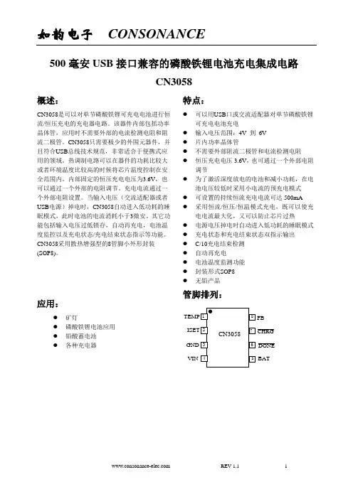
500毫安USB接口兼容的锂电池充电集成电路CN3062
- 格式:pdf
- 大小:377.81 KB
- 文档页数:11
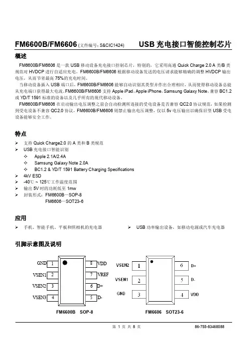
FM6600B/FM6606 (文件编号:S&CIC1424) USB充电接口智能控制芯片概述FM6600B/FM6606是一款USB移动设备充电接口控制芯片,特别的,它采用高通Quick Charge 2.0 A类/B类规范对HVDCP进行自适应充电。
FM6600B/FM6606根据移动设备发送的电压请求能够精确的调整HVDCP输出电压,从而节省最高75%的充电时间。
当移动设备插入USB端口后,FM6600B/FM6606能够自动识别其类型并作出合理相应,从而使得移动设备总能从充电端口获得最大电流。
FM6600B/FM6606支持Apple iPad,Apple iPhone,Samsung Galaxy Note,兼容BC1.2或YD/T 1591标准的设备以及几乎所有的现代移动设备。
FM6600B/FM6606在启动输出电压调整之前会自动检测所连接的受电设备是否兼容QC2.0协议规范,如果检测到受电设备不兼容QC2.0协议,FM6600B/FM6606则禁止输出电压调整,仅以5v电压输出以确保旧型USB受电设备能够安全工作。
特点支持Quick Charge2.0的A类和B类规范USB充电接口智能识别✧Apple 2.1A/2.4A✧Samsung Galaxy Note 2.0ACVREFB(文件编号:S&CIC1424)内部框图FM6600B/FM6606 (文件编号:S&CIC1424) USB充电接口智能控制芯片极限工作条件*注意:如果器件工作条件超过上述各项极限值,可能对器件造成永久性损坏。
上述参数仅是工作条件的极限值,不建议器件工作在推荐工作条件以外的情况。
器件长时间工作在极限工作条件下,其可靠性可能受到影响。
推荐工作条件电气参数(文件编号:S&CIC1424)FM6600B/FM6606 (文件编号:S&CIC1424) USB充电接口智能控制芯片典型应用电路图FM6600BFM6600B/FM6606 (文件编号:S&CIC1424) USB充电接口智能控制芯片FM6606电路功能描述FM6600B/FM6606是一款支持Quick Charge 2.0规范的USB高压专用充电端口(HVDCP)的智能接口IC,它能够自动识别连接到USB端口的受电设备类型,从而允许受电设备以所需的充电电压从充电端口获得最大电流。
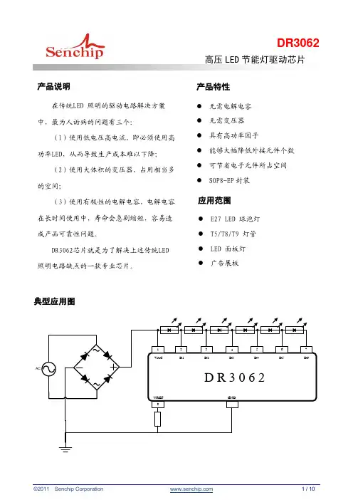
南京拓品微电子有限公司NanJing Top Power ASIC Corp.数据手册DATASHEETTP4057(500mA线性锂离子电池充电器)概述、特点、典型应用-------------------------------------------------------------------------------------P2管脚、特性指标----------------------------------------------------------------------------------------------P3引脚功能说明-------------------------------------------------------------------------------------------------P5充电电流大小设置、电池反接保护功能----------------------------------------------------------------P7充电指示状态、无电池连接指示状态-------------------------------------------------------------------P8多种典型应用图、使用注意事项-------------------------------------------------------------------------P12采用SOT23封装500mA 防锂电池反接充电器Top Power ASIC拓品微电子特点·锂电池正负极反接保护; ·高达500mA 的可编程充电电流; ·无需MOSFET 、检测电阻器或隔离二极管; ·用于单节锂离子电池 ·恒定电流/恒定电压操作,并具有可在无过热危险的情况下实现充电速率最大化的热调节功能;·可直接从USB 端口给单节锂离子电池充电; ·精度达到±1%的4.2V 预设充电电压; ·最高输入可达9V ; ·自动再充电;·2个充电状态开漏输出引脚; ·C/10充电终止;·待机模式下的供电电流为40uA ; ·2.9V 涓流充电器件版本; ·软启动限制了浪涌电流; ·采用6引脚SOT-23封装。
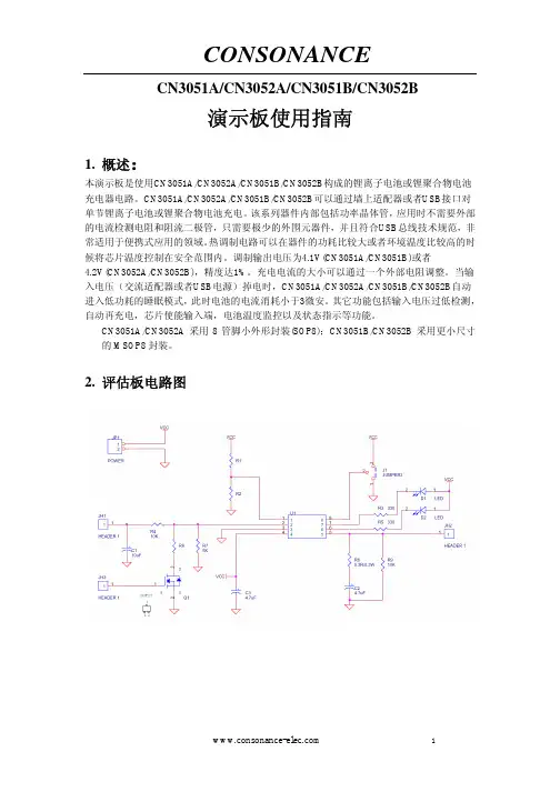
CN3051A/CN3052A/CN3051B/CN3052B演示板使用指南1. 概述:本演示板是使用CN3051A/CN3052A/CN3051B/CN3052B构成的锂离子电池或锂聚合物电池充电器电路。
CN3051A/CN3052A/CN3051B/CN3052B可以通过墙上适配器或者USB接口对单节锂离子电池或锂聚合物电池充电。
该系列器件内部包括功率晶体管,应用时不需要外部的电流检测电阻和阻流二极管,只需要极少的外围元器件,并且符合USB总线技术规范,非常适用于便携式应用的领域。
热调制电路可以在器件的功耗比较大或者环境温度比较高的时候将芯片温度控制在安全范围内。
调制输出电压为4.1V(CN3051A/CN3051B)或者4.2V(CN3052A/CN3052B),精度达1%。
充电电流的大小可以通过一个外部电阻调整。
当输入电压(交流适配器或者USB电源)掉电时,CN3051A/CN3052A/CN3051B/CN3052B自动进入低功耗的睡眠模式,此时电池的电流消耗小于3微安。
其它功能包括输入电压过低检测,自动再充电,芯片使能输入端,电池温度监控以及状态指示等功能。
CN3051A/CN3052A采用8管脚小外形封装(SOP8);CN3051B/CN3052B采用更小尺寸的MSOP8封装。
2. 评估板电路图3. 元器件列表及注意事项序号 名称 描述1 JP1 输入电源接入插头。
在VCC 和GND 之间施加4.35V 到6V 的电压。
2 JH1 CN3051A/B/CN3052A/B 第2管脚ISET 电压监测点。
通过此点监测可以避免测试仪器的分布电容对CN3051A/B/CN3052A/B 第2管脚电压的影响。
3 JH2 CN3051A/B/CN3052A/B 第5管脚BAT 引出点。
电池接入端,充电电流和充电电压也从此点输出。
4 JH3 MOS 晶体管Q1栅极输入端。
输入高电平将扩流电阻R6接入电路,充电电流增大。
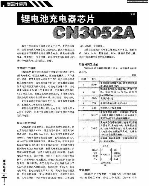
高性能的线性锂电池充电管理芯片CN3052A/CN3052B/CN3056的应用CN3052A/CN3052B/CN3056是高性能的线性锂电池充电管理芯片。
这些器件内部集成有功率管,不需要外部的电流检测电阻和阻流二极管,只需要极少的外围元器件,并且符合USB总线技术规范,可以通过USB端口为锂电池充电,因此非常适用于各种充电器及MP4播放器、蓝牙耳机、数码相机等便携式产品。
图1是一个典型的应用电路图。
图1:CN3052A/CN3052B/CN3056的典型应用电路图CN3052A/CN3052B/CN3056的工作流程图2是CN3052A/CN3052B/CN3056的充电过程示意图。
当输入电压大于电源低电压检测阈值和芯片使能输入端接高电平时,CN3052A/CN3052B/CN3056开始对电池充电,CHRG管脚输出低电平,表示充电正在进行。
如果电池电压低于3V,充电器用小电流对电池进行预充电。
当电池电压超过3V时,充电器采用恒流模式对电池充电,充电电流由ISET管脚和GND之间的电阻RISET<确定。
当电池电压接近电池端调制电压4.2V时,充电电流逐渐减小,CN3052A/CN3052B/CN3056进入恒压充电模式。
图2:CN3052A/CN3052B/CN3056充电过程示意图当充电电流减小到充电结束阈值时,CHRG端输出高阻态,表示充电周期结束,充电结束阈值是恒流充电电流的10%。
如果要开始新的充电周期,只要将输入电压断电,然后再上电就可以了,或者将CE管脚的电压暂时拉到0V,再恢复到高电平。
当电池电压降到再充电阈值以下时,自动开始新的充电周期。
当输入电压低于电池电压时,充电器进入低功耗的睡眠模式,电池端消耗的电流小于3uA,从而增加了待机时间。
如果将使能输入端CE接低电平,充电器被关断。
CN3052A/CN3052B/CN3056的主要功能介绍电源低电压检测(UVLO) CN3052A/CN3052B/CN3056内部有电源电压检测电路,当电源电压低于电源电压过低阈值(典型值4.03V)时,芯片处于关断状态,充电也被禁止。
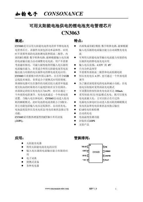
Lithium Ion Battery Charger for Solar-Powered SystemsCN3063General Description:The CN3063 is a complete constant-current /constant voltage linear charger for single cell Li-ion and Li Polymer rechargeable batteries. The device contains an on-chip power MOSFET and eliminates the need for the external sense resistor and blocking diode. An on-chip 8-bit ADC can adjust charging current automatically based on the output capability of input power supply, so CN3063 is ideally suited for solar powered system. Furthermore, the CN3063 is specifically designed to work within USB power specifications. Thermal feedback regulates the charge current to limit the die temperature during high power operation or high ambient temperature. The regulation voltage is internally fixed at 4.2V with 1% accuracy, it can also be adjusted with an external resistor. The charge current can be programmed externally with a single resistor. When the input supply is removed, the CN3063 automatically enters a low power sleep mode , dropping the battery drain current to less than 3uA. Other features include undervoltage lockout, automatic recharge, battery temperature sensing and charging/termination indicator.The CN3063 is available in a thermally enhanced8-pin SOP package.Applications:●Solar Powered System●Digital Still Cameras●MP3 Players●Bluetooth Applications●Portable Devices●Chargers Features:●On-chip 8-bit ADC can adjust charging currentautomatically based on the output capability ofinput power supply●Suitable for Solar-Powered System●On-chip Power MOSFET●No external Blocking Diode or Current SenseResistors Required●Preset 4.2V Regulation V oltage with 1%Accuracy, adjustable with an external resistor●Precharge Conditioning for Reviving DeeplyDischarged Cells and Minimizing Heat Dissipation During Initial Stage of Charge●Continuous Programmable Charge Current Upto 600mA●Constant-Current/Constant-Voltage Operationwith Thermal Regulation to Maximize ChargeRate Without Risk of Overheating●Automatic Low-Power Sleep Mode When InputSupply Voltage is Removed●Status Indication for LEDs or uP Interface●C/10 Charge Termination●Automatic Recharge●Battery Temperature Sensing●Available in SOP8 Package●Pb-free AvailablePin AssignmentFBGNDVIN BATCHRGDONETypical Application CircuitInput Power Supply 4.4V to 6VFigure 1 Typical Application Circuit(Constant V oltage Level 4.2V) Input Power Supply 4.4V to 6VFigure 2 Application Circuit(Adjust Constant V oltage Level with Rx)In Figure 2, the BAT pin’s voltage in constant voltage mode is given by the following equation:Vbat = 4.2+3.04×10⁻⁶×RxWhere,Vbat is in voltRx is in ohmBlock DiagramFigure 3 Block DiagramPin DescriptionPin No. Name Function Description1 TEMPTemperature Sense Input. Connecting TEMP pin to NTC thermistor’soutput in Lithium ion battery pack. If TEMP pin’s voltage is below 46% ofinput supply voltage V IN for more than 0.15S, this means that battery’stemperature is too high or too low, charging is suspended. If TEMP’s voltagelevel is above 46% of input supply voltage for more than 0.15S, battery faultstate is released, and charging will resume.The temperature sense function can be disabled by grounding the TEMP pin.2 ISETConstant Charge Current Setting and Charge Current Monitor Pin. Thecharge current is set by connecting a resistor R ISET from this pin to GND.When in precharge mode, the ISET pin’s voltage is regulated to 0.2V. When inconstant charge current mode, the ISET pin’s voltage is regulated to 2V. In allmodes during charging, the voltage on ISET pin can be used to measure thecharge current as follows:I CH = (V ISET/R ISET)×9003 GNDGround Terminal.4 VINPositive Input Supply Voltage. V IN is the power supply to the internal circuit.When V IN drops to within 40mv of the BAT pin voltage, CN3063 enters lowpower sleep mode, dropping BAT pin’s current to less than 3uA.5 BATBattery Connection Pin. Connect the positive terminal of the battery to BATpin. BAT pin draws less than 3uA current in chip disable mode or in sleepmode. BAT pin provides charge current to the battery and provides regulationvoltage of 4.2V.6Open-Drain Charge termination Status Output. In charge terminationstatus, is pulled low by an internal switch; Otherwise pin is inhigh impedance state.7Open Drain Charge Status Output. When the battery is being charged, thepin is pulled low by an internal switch, otherwise pin is in highimpedance state.8 FBBattery Voltage Kevin Sense Input. This Pin can Kelvin sense the batteryvoltage; Also the regulation voltage in constant voltage mode can be adjustedby connecting an external resistor between FB pin and BAT pin. Absolute Maximum RatingsAll Terminal V oltage……………-0.3V to 6.5V Maximum Junction Temperature…...150℃BAT Short-Circuit Duration………...Continuous Operating Temperature…...-40℃ to 85℃Storage Temperature….............-65℃ to 150℃ Thermal Resistance (SOP8)………….TBDLead Temperature(Soldering)…….............300℃Stresses beyond those listed under ‘Absolute Maximum Ratings’ may cause permanent damage to the device. These are stress ratings only and functional operation of the device at these or any other conditions above those indicated in the operational sections of the specifications is not implied. Exposure to Absolute Maximum Rating Conditions for extended periods may affect device reliability.Electrical Characteristics(VIN=5V, T A=-40℃ to 85℃, Typical Values are measured at T A=25℃,unless otherwise noted) Parameters Symbol TestConditions Min Typ Max Unit Input Supply Voltage VIN 4.4 6 V Operating Current I VIN Charge Termination Mode 400 650 950uA Undervoltage Lockout Vuvlo VIN falling 3.7 3.9V Undervoltage LockoutHysteresisHuvlo 0.1 V Regulation Voltage V REG Constant Voltage Mode 4.158 4.2 4.242 VR ISET=3.6K, V BAT=3.6V 400 500 600R ISET=3.6K, V BAT=2.4V25 50 75mAV BAT=V REG, standby mode 1.75 3.5 7 BAT pin Current I BATVIN=0V, sleep mode 3uA Precharge ThresholdPrecharge Threshold V PRE Voltage at BAT pin rising 2.9 3.0 3.1 VPrecharge Threshold Hysteresis H PRE 0.1VCharge Termination ThresholdCharge TerminationThresholdVterm Measure voltage at ISET pin 0.18 0.22 0.26 V Recharge ThresholdRecharge Threshold V RECH V REG-0.1 V Sleep ModeSleep Mode Threshold V SLP V IN from high to low, measuresthe voltage (V IN-V BAT)40 mvSleep mode Release Threshold V SLPRV IN from low to high, measuresthe voltage (V IN-V BAT)90 mvISET PinPrecharge mode 0.2ISET Pin Voltage V ISETConstant current mode 2.0VTEMP PINInput Threshold V TEMP43.5 46 48.5%V INTEMP input Current TEMP to V IN or to GND 0.5uAPinSink Current I DONE V DONE=0.3V, termination mode 10 mA Leakage Current V DONE=6V, charge mode 1 uAPinSink Current I CHRG V CHRG=0.3V, Charge status 10 mALeakage Current V CHRG=6V, termination mode 1 uADetailed DescriptionThe CN3063 is a linear battery charger designed primarily for charging single cell lithium-ion orlithium-polymer batteries. Featuring an internal P-channel power MOSFET, the charger uses aconstant-current/constant-voltage to charge the batteries. Continuous charge current can be programmed up to 600mA with an external resistor. No blocking diode or sense resistor is required. The on-chip 8-bit ADC can adjust charging current automatically based on the output capability of input power supply, so CN3063 is ideally suited for the solar-powered systems, or the applications that need to charge lithium-ion battery or lithiumpolymer battery with an input power supply whose output capability is limited. The open-drain outputand indicates the charger’s status. The internal thermal regulation circuit reduces the programmed charge current if the die temperature attempts to rise above a preset value of approximately 115℃. This feature protects the CN3063 from excessive temperature, and allows the user to push the limits of the power handling capability of a given circuit board without risk of damaging the CN3063 or the external components. Another benefit of adopting thermal regulation is that charge current can be set according to typical, not worst-case, ambient temperatures for a given application with the assurance that the charger will automatically reduce the current in worst-case conditions.The charge cycle begins when the voltage at the V IN pin rises above the UVLO level, a current set resistor isconnected from the ISET pin to ground. The pin outputs a logic low to indicate that the charge cycle is ongoing. At the beginning of the charge cycle, if the voltage at FB pin is below 3V, the charger is in precharge mode to bring the cell voltage up to a safe level for charging. The charger goes into the fast chargeconstant-current mode once the voltage on the FB pin rises above 3V. In constant current mode, the charge current is set by R ISET. When the battery approaches the regulation voltage, the charge current begins to decrease as the CN3063 enters the constant-voltage mode. When the current drops to charge termination threshold, thecharge cycle is terminated, is pulled low by an internal switch and pin assumes a high impedance state to indicate that the charge cycle is terminated. The charge termination threshold is 10% of the current in constant current mode. To restart the charge cycle, just remove the input voltage and reapply it. The charge cycle can also be automatically restarted if the FB pin voltage falls below the recharge threshold. The on-chip reference voltage, error amplifier and the resistor divider provide regulation voltage with 1% accuracy which can meet the requirement of lithium-ion and lithium polymer batteries. When the input voltage is not present, the charger goes into a sleep mode, dropping battery drain current to less than 3uA. This greatly reduces the current drain on the battery and increases the standby time.The charging profile is shown in the following figure:Charge CurrentBattery VoltageFigure 4 Charging ProfileApplication InformationUndervoltage Lockout (UVLO)An internal undervoltage lockout circuit monitors the input voltage and keeps the charger in shutdown mode until V IN rises above the undervoltage lockout voltage. The UVLO circuit has a built-in hysteresis of 0.1V. Sleep modeThere is an on-chip sleep comparator. The comparator keeps the charger in sleep mode if V IN falls below sleep mode threshold(VBAT+40mv). Once in sleep mode, the charger will not come out of sleep mode until V IN rises 90mv above the battery voltage.Precharge modeAt the beginning of a charge cycle, if the battery voltage is below 3V, the charger goes into precharge mode , and the charge current is 10% of fast charge current in constant current mode.Charging Current limited by the Output capability of Input Power SupplyIf the output capability of input power supply is less than the charging current set by the resistor at ISET pin, then the on-chip 8-bit ADC will begin to function to adjust the charging current based on the output capability of input power supply. In this case, the charging current may be less than the value set by the resistor at ISET pin, but it is maximized to the output capability of input power supply on the condition that the input voltage at VIN pin is no less than 4.35V, which is the minimum operating voltage of CN3063. So the charging current can be set according to the maximum output capability of input power supply, not the worst case.Adjusting the regulation voltage in constant voltage modeThe regulation voltage in constant voltage mode can be adjusted by an external resistor connecting between FB pin and BAT pin as shown in Figure 5:Figure 5 Adjusting Regulation V oltage in Constant V oltage ModeIn Figure 5, the regulation voltage in constant voltage mode will be given by the following equation:Vbat = 4.2+3.04×10⁻⁶×RxWhere,Vbat is in voltRx is in ohmProgramming Charge CurrentThe formula for the battery charge current in constant current mode is:I CH = 1800V / R ISETWhere:I CH is the charge current in ampereR ISET is the total resistance from the ISET pin to ground in ohmFor example, if 500mA charge current is required, calculate:R ISET = 1800V/0.5A = 3.6kΩFor best stability over temperature and time, 1% metal film resistors are recommended. If the charger is in constant-temperature or constant voltage mode, the charge current can be monitored by measuring the ISET pin voltage, and the charge current is calculated as the following equation:I CH = (V ISET / R ISET) × 900Combine Two Power InputsAlthough the CN3063 allows charging from a solar power supply, a wall adapter or a USB port can also be used to charge Li-Ion/Li-polymer batteries. Figure 6 shows an example of how to combine 2 power inputs. AP-channel MOSFET, M1, is used to prevent back conducting into the 2nd power supply when the 1st power supply is present and Schottky diode, D1, is used to prevent 2nd power supply loss through the 1kΩ pull-down resistor.1st power supply supplyFigure 6Combining 2 Input Power SupplyBattery Temperature SenseTo prevent the damage caused by the very high or very low temperature done to the battery pack, the CN3063 continuously senses battery pack temperature by measuring the voltage at TEMP pin.If V TEMP <(46%×VIN) for 0.15 seconds, it indicates that the battery temperature is too high or too low and the charge cycle is suspended. If V TEMP >(46%×VIN) for 0.15 seconds, the charge cycle resumes. The battery temperature sense function can be disabled by connecting TEMP pin to GND.RechargeAfter a charge cycle has terminated, if the battery voltage drops below the recharge threshold of 4.1V, a new charge cycle will begin automatically.Constant-Current/Constant-Voltage/Constant-TemperatureThe CN3063 use a unique architecture to charge a battery in a constant-current, constant-voltage, constant temperature fashion as shown in Figure 3. Amplifiers Iamp, Vamp, and Tamp are used in three separatefeedback loops to force the charger into constant-current, constant-voltage, or constant-temperature mode, respectively. In constant current mode the charge current delivered to the battery equal to 1800V/R ISET . If the power dissipation of the CN3063 results in the junction temperature approaching 115℃, the amplifier Tamp will begin decreasing the charge current to limit the die temperature to approximately 115℃. As the battery voltage rises, the CN3063 either returns to constant-current mode or it enters constant voltage mode straight from constant-temperature mode.Open-Drain Status OutputsThe CN3063 have 2 open-drain status outputs:and . is pulled low when the charger is incharging status, otherwisebecomes high impedance. is pulled low if the charger is in charge termination status, otherwisebecomes high impedance. When the battery is not present, the charger charges the output capacitor to the regulation voltage quickly, then the BAT pin’s voltage decays slowly to recharge threshold because of low leakage current at BAT pin, which results in a 100mv ripple waveform at BAT pin, in the meantime, pin outputs a pulse to indicate that the battery’s absence. The pulse’s frequency is around 10Hz when a 4.7uF output capacitor is used. The open drain status output that is not used should be tied to ground.V IN Bypass Capacitor C INMany types of capacitors can be used for input bypassing, C IN is typically a 22uF capacitor.For the consideration of the bypass capacitor, please refer to the Application Note AN102 from our website.StabilityTypically a 4.7uF capacitor from BAT pin to GND is required to stabilize the feedback loop.In constant current mode, the stability is also affected by the impedance at the ISET pin . With no additional capacitance on the ISET pin, the loop is stable with current set resistors values as high as 50KΩ. However, additional capacitance on ISET pin reduces the maximum allowed current set resistor. The pole frequency at ISET pin should be kept above 200KHz. Therefore, if ISET pin is loaded with a capacitance C, the following equation should be used to calculate the maximum resistance value for R ISET:R ISET < 1/(6.28×2×105×C)In order to measure average charge current or isolate capacitive load from ISET pin, a simple RC filter can be used on ISET pin as shown in Figure 7.Figure 7 Isolating Capacitive Load on ISET PinBoard Layout Considerations1.R ISET at ISET pin should be as close to CN3063 as possible, also the parasitic capacitance at ISET pinshould be kept as small as possible.2.The capacitance at VIN pin and BAT pin should be as close to CN3063 as possible.3.During charging, CN3063’s temperature may be high, the NTC thermistor should be placed far enough toCN3063 so that the thermistor can reflect the battery’s temperature correctly.4.It is very important to use a good thermal PC board layout to maximize charging current. The thermal pathfor the heat generated by the IC is from the die to the copper lead frame through the package lead(especially the ground lead) to the PC board copper, the PC board copper is the heat sink. The footprint copper pads should be as wide as possible and expand out to larger copper areas to spread and dissipate the heat to the surrounding ambient. Feedthrough vias to inner or backside copper layers are also useful in improving the overall thermal performance of the charger. Other heat sources on the board, not related to the charger, must also be considered when designing a PC board layout because they will affect overall temperature rise and the maximum charge current.The ability to deliver maximum charge current under all conditions require that the exposed metal pad on the back side of the CN3063 package be soldered to the PC board ground. Failure to make the thermal contact between the exposed pad on the backside of the package and the copper board will result in larger thermal resistance.Package InformationConsonance does not assume any responsibility for use of any circuitry described. Consonance reserves the right to change the circuitry and specifications without notice at any time.REV 1.1 11。
南京拓微集成电路有限公司NanJing Top Power ASIC Corp.数据手册DATASHEETTP51002A开关降压8.4V/4.2V锂电池充电器芯片概述TP5100是一款开关降压型双节8.4V/单节4.2V 锂电池充电管理芯片。
其QFN16超小型封装与简单的外围电路,使得TP5100非常适用于便携式设备的大电流充电管理应用。
同时,TP5100内置输入过流、欠压保护、芯片过温保护、短路保护、电池温度监控。
TP5100具有5V-12V 输入电压,对电池充电分为涓流预充、恒流、恒压三个阶段,涓流预充电电流、恒流充电电流都通过外部电阻调整,最大充电电流达2A 。
TP5100采用频率400kHz 的开关工作模式使它可以使用较小的外围器件,并在大电流充电中仍保持较小的发热量。
TP5100内置功率PMOSFET 、防倒灌电路,所以无需防倒灌肖特基二极管等外围保护。
特性■双/单节8.4V/4.2V 锂电池充电■内置功率MOSFET,开关型工作模式,器件发热少,外围简单■可编程充电电流,0.1A--2A ■可编程预充电电流,20%--100%■红绿LED 充电状态指示■芯片温度保护,过流保护,欠压保护■电池温度保护、电池短路保护■开关频率400KHz ,可用电感4.7uH-22uH ■PWR_ON-电源、电池供电切换控制■小于1%的充电电压控制精度■涓流、恒流、恒压三段充电,保护电池■采用QFN16 4mm*4mm 超小型封装绝对最大额定值■静态输入电源电压(VIN ):18V ■BA T :0V ~9V■BA T 短路持续时间:连续■最大结温:120℃■工作环境温度范围:-20℃~85℃■贮存温度范围:-30℃~125℃■引脚温度(焊接时间10秒):260℃应用■便携式设备、各种充电器■智能手机、PDA 、移动蜂窝电话■MP4、MP5播放器、平板电脑■航模、电动工具、对讲机典型应用VINBATTP5100CHRGSTDBY LXVSVIN=12V10uF1K1415 1. 4. 5. 162.3897GND TS1110u F10uHRs=0.06710u FVS 8.4V 2SLiG RCSR N T CR 1VREG RTRICK0.1uF1012130.1uF0.1u F0.1u FPWR_ON-6BAT+S S 34R 250K0.2Ω(建议两个0.4并联,1206封装)3Ω0.1nF 图1 TP5100为8.4V 双节锂离子电池1.5A 充电应用示意图(如需更高耐压,LX 端RC 电路需接入)VINBATTP5100CHRGSTDBYLXVSVIN=5-12V10uF1K1415 1. 4. 5. 162.3897GND TS1110u F10uHRs=0.06710u FVS4.2V LiG RCSR N T CR 1VREG RTRICK0.1uF1012130.1uF0.1u F0.1u FPWR_ON-6BAT+S S 34R 250K3Ω0.1nF 0.2Ω(建议两个0.4并联,1206封装)图2 TP5100为4.2V 单节锂离子电池1.5A 充电应用示意图封装/订购信息16引脚4mm*4mmQFN16封装顶视图(散热片接地)订单型号TP5100-QFN16器件标记 TP5100 实物图片TP5100功能方框图图3 TP5100功能框图电特性表1 TP5100电特性能参数凡注●表示该指标适合8.4V 、4.2V 模式,否则仅指8.4V ,T A =25℃,VIN=9V ,除特别注明。