串口标准ANSI_TIA_EIA-232-F
- 格式:pdf
- 大小:18.51 MB
- 文档页数:47
电源接口部分用8.4V镍氢电池组为其供电,通过两片LM7805稳压芯片进行分频,分别有两种电压值输出为5V,12V。
从而满足系统板供电要求。
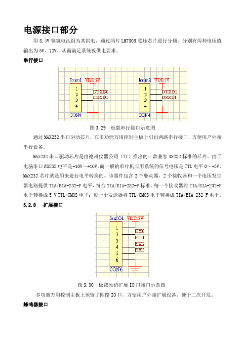
串行接口图3.29 板载串行接口示意图通过MAX232串口驱动芯片,在多功能万用控制主板上引出两路串行接口,方便用户外接串行设备。
MAX232串口驱动芯片是由德州仪器公司(TI)推出的一款兼容RS232标准的芯片。
由于电脑串口RS232电平是-10V~+10V,而一般的单片机应用系统的信号电压是TTL电平0~+5V,MAX232芯片就是用来进行电平转换的。
该器件包含2个驱动器、2个接收器和一个电压发生器电路提供TIA/EIA-232-F电平,符合TIA/EIA-232-F标准。
每一个接收器将TIA/EIA-232-F 电平转换成5-V TTL/CMOS电平;每一个发送器将TTL/CMOS电平转换成TIA/EIA-232-F电平。
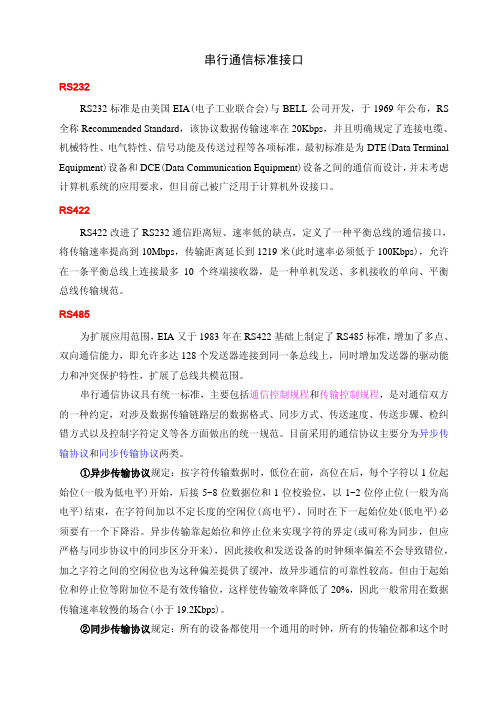
3.2.8 扩展接口图3.30 板载预留扩展IO口接口示意图多功能万用控制主板上预留了四路IO口,方便用户外接扩展设备,便于二次开发。
蜂鸣器接口板载蜂鸣器接口示意图板载蜂鸣器,起到提示的作用,当传感器工作时有提示声音,下载程序时,蜂鸣器发声,提示下载成功。
直流电机接口电机驱动芯片(L298N)图3.33 四路电机接口板载四路直流电机接口,用于给小车提供足够的动力来源。
采用两片L298N电机驱动芯片,其中每一片L298N均可驱动两路直流电机。
L298N内部包含4通道逻辑驱动电路。
可以方便的驱动两个直流电机,或一个两相步进电机。
L298N芯片可以驱动两个二相电机,也可以驱动一个四相电机,输出电压最高可达50V,可以直接通过电源来调节输出电压;可以直接用单片机的IO口提供信号;而且电路简单,使用比较方便。
恒速电机接口板载恒速电机接口示意图板载两路恒速电机接口,可用于外接小型直流电机。
步进电机接口板载步进电机接口示意图主板预留步进电机接口,可外接两路步进电机,用于完成控制步进电机的正转、反转、转动角度以及转动速度。

DESCRIPTIONs Meets true EIA/TIA-232-F Standards from a +3.0V to +5.5V power supplys 235KBps Transmission Rate Under Load s 1µA Low-Power Shutdown with Receivers Active (SP3222E )s Interoperable with RS-232 down to +2.7V power sources Enhanced ESD Specifications: ±15kV Human Body Model±15kV IEC1000-4-2 Air Discharge ±8kV IEC1000-4-2 Contact DischargeThe SP3222E/3232E series is an RS-232 transceiver solution intended for portable or hand-held applications such as notebook or palmtop computers. The SP3222E/3232E series has a high-efficiency, charge-pump power supply that requires only 0.1µF capacitors in 3.3V operation. This charge pump allows the SP3222E/3232E series to deliver true RS-232performance from a single power supply ranging from +3.3V to +5.0V. The SP3222E/3232E are 2-driver/2-receiver devices. This series is ideal for portable or hand-held applications such as notebook or palmtop computers. The ESD tolerance of the SP3222E/3232E devices are over ±15kV for both Human Body Model and IEC1000-4-2 Air discharge test methods. The SP3222E device has a low-power shutdown mode where the devices' driver outputs and charge pumps are disabled. During shutdown, the supply current falls to less than 1µA.SELECTION TABLEL E D O M s e i l p p u S r e w o P 232-S R s r D e v i r 232-S R sr e v i e c e R l a n r e t x E st n e n o p m o C nw o d t u h S L T T a S -3e t t f o .o N s n i P 2223P S V 5.5+o t V 0.3+224s e Y s e Y 02,812323P S V5.5+o t V 0.3+224oN oN 61RE T E M A R A P .N I M .P Y T .X A M ST I N U SN O I T I D N O C S C I T S I R E T C A R A H C C D tn e r r u C y l p p u S 3.00.1A m T ,d a o l o n B M A 52+=o V ,C C C V 3.3=tn e r r u C y l p p u S n w o d t u h S 0.101µA,D N G =N D H S T B M A 52+=o V ,C C C V3.3+=S T U P T U O R E V I E C E R D N A S T U P N I C I G O L W O L d l o h s e r h T c i g o L t u p n I 8.0V 2e t o N ,N D H S ,N E ,N I x T H G I H d l o h s e r h T c i g o L t u p n I 0.24.2V V C C 2e t o N ,V 3.3=V C C 2e t o N ,V 0.5=t n e r r u C e g a k a e L t u p n I 10.0±0.1±µA ,N D H S ,N E ,N I x T T B M A 52+=o C t n e r r u C e g a k a e L t u p t u O 50.0±01±µA d e l b a s i d s r e v i e c e r W O L e g a t l o V t u p t u O 4.0V I T U O A m 6.1=H G I H e g a t l o V t u p t u O V C C 6.0-V C C 1.0-VI T U O Am 0.1-=S T U P T U O R E V I R D gn i w S e g a t l o V t u p t u O 0.5±4.5±Vk 3Ω,s t u p t u o r e v i r d l l a t a d n u o r g o t d a o l T B M A 52+=o Cec n a t s i s e R t u p t u O 003ΩV C C T ,V 0=-V =+V =T U O =+V 2t n e r r u C t i u c r i C -t r o h S t u p t u O 53±07±06±001±A m A m V T U O V 0=V T U O =+V51tn e r r u C e g a k a e L t u p t u O 52±µAV T U O =+V ,V 21C C de l b a s i d s r e v i r d ,V 5.5o t V 0=NOTE 1: V+ and V- can have maximum magnitudes of 7V, but their absolute difference cannot exceed 13V.ABSOLUTE MAXIMUM RATINGSThese are stress ratings only and functional operation of the device at these ratings or any other above those indicated in the operation sections of the specifications below is not implied. Exposure to absolute maximum rating conditions for extended periods of time may affect reliability and cause permanent damage to the device.V CC ................................................................-0.3V to +6.0V V+ (NOTE 1)................................................-0.3V to +7.0V V- (NOTE 1)................................................+0.3V to -7.0V V+ + |V-| (NOTE 1)....................................................+13V I CC (DC V CC or GND current).................................±100mAInput VoltagesTxIN, EN .....................................................-0.3V to +6.0V RxIN.............................................................................±25V Output VoltagesTxOUT.....................................................................±13.2V RxOUT..............................................-0.3V to (V CC + 0.3V)Short-Circuit DurationTxOUT...............................................................Continuous Storage Temperature.................................-65°C to +150°C Power Dissipation Per Package20-pin SSOP (derate 9.25mW/o C above +70o C).....750mW 18-pin PDIP (derate 15.2mW/o C above +70o C)....1220mW 18-pin SOIC (derate 15.7mW/o C above +70o C)...1260mW 20-pin TSSOP (derate 11.1mW/o C above +70o C)..890mW 16-pin SSOP (derate 9.69mW/o C above +70o C).....775mW 16-pin PDIP (derate 14.3mW/o C above +70o C)....1150mW 16-pin Wide SOIC (derate 11.2mW/o C above +70o C)900mW 16-pin TSSOP (derate 10.5mW/o C above +70o C)..850mW 16-pin nSOIC (derate 13.57mW/°C above +70°C)..1086mWSPECIFICATIONSUnless otherwise noted, the following specifications apply for V CC = +3.0V to +5.0V with T AMB = T MIN to T MAXR E T E M A R A P .N I M .P Y T .X A M ST I N U SN O I T I D N O C S T U P N I R E V I E C E R e g n a R e g a t l o V t u p n I 51-51+V W O L d l o h s e r h T t u p n I 6.08.02.15.1V V C C V 3.3=V C C V 0.5=H G I H d l o h s e r h T t u p n I 5.18.14.24.2V V C C V 3.3=V C C V0.5=s i s e r e t s y H t u p n I 3.0V ec n a t s i s e R t u p n I 357k ΩS C I T S I R E T C A R A H C G N I M I T e t a R a t a D m u m i x a M 021532s p b k R L k 3=ΩC ,L g n i h c t i w s r e v i r d e n o ,F p 0001=y a l e D n o i t a g a p o r P r e v i r D 0.10.1µs µs t L H P R ,L K 3=ΩC ,L F p 0001=t H L P R ,L K 3=ΩC ,L F p 0001=y a l e D n o i t a g a p o r P r e v i e c e R 3.03.0µs t L H P C ,T U O x R o t N I x R ,L F p 051=t H L P C ,T U O x R o t N I x R ,L Fp 051=e m i T e l b a n E t u p t u O r e v i e c e R 002s n e m i T e l b a s i D t u p t u O r e v i e c e R 002s n w e k S r e v i r D 001005s n t |L H P t -H L P T ,|B M A 52=o C we k S r e v i e c e R 0020001s n t |L H P t -H L P |et a R w e l S n o i g e R -n o i t i s n a r T 03/V µsV C C R ,V 3.3=L K 3=ΩT ,B M A 52=o ,C V 0.3+o t V 0.3-m o r f n e k a t s t n e m e r u s a e m V0.3-o t V 0.3+r o SPECIFICATIONS (continued)Unless otherwise noted, the following specifications apply for V CC = +3.0V to +5.0V with T AMB = T MIN to T MAX .Typical Values apply at V CC = +3.3V or +5.0V and T AMB = 25o C.NOTE 2: Driver input hysteresis is typically 250mV.Capacitance for the SP3222 and the SP3232SP3222 and the SP3232Transmitting Data for the SP3222 and the SP3232TYPICAL PERFORMANCE CHARACTERISTICSUnless otherwise noted, the following performance characteristics apply for V CC = +3.3V, 235kbps data rates, all drivers loaded with 3k Ω, 0.1µF charge pump capacitors, and T AMB = +25°C.DESCRIPTIONThe SP3222E/3232E transceivers meet the EIA/TIA-232 and V.28/V.24 communication proto-cols and can be implemented in battery-pow-ered, portable, or hand-held applications such as notebook or palmtop computers. The SP3222E/3232E devices all feature Sipex's proprietary on-board charge pump circuitry that generates 2x V CC for RS-232 voltage levels from a single +3.0V to +5.5V power supply. This series is ideal for +3.3V-only systems, mixed +3.3V to +5.5V systems, or +5.0V-only systems that re-quire true RS-232 performance. The SP3222E/3232E series have drivers that operate at a typi-cal data rate of 235Kbps fully loaded.The SP3222E and SP3232E are 2-driver/2-re-ceiver devices ideal for portable or hand-held applications. The SP3222E features a 1µA shutdown mode that reduces power consump-tion and extends battery life in portable systems.Its receivers remain active in shutdown mode,allowing external devices such as modems to be monitored using only 1µA supply current.THEORY OF OPERATIONThe SP3222E/3232E series are made up of three basic circuit blocks: 1. Drivers, 2. Receivers,and 3. the Sipex proprietary charge pump.DriversThe drivers are inverting level transmitters that convert TTL or CMOS logic levels to ±5.0V EIA/TIA-232 levels inverted relative to the in-put logic levels. Typically, the RS-232 output voltage swing is ±5.5V with no load and at least ±5V minimum fully loaded. The driver outputs are protected against infinite short-circuits to ground without degradation in reliability. Driver outputs will meet EIA/TIA-562 levels of ±3.7V with supply voltages as low as 2.7V.The drivers typically can operate at a data rate of 235Kbps. The drivers can guarantee a data rate of 120Kbps fully loaded with 3K Ω in parallel with 1000pF, ensuring compatibility with PC-to-PC communication software.The slew rate of the driver output is internally limited to a maximum of 30V/µs in order to meet the EIA standards (EIA RS-232D 2.1.7, Para-graph 5). The transition of the loaded output from HIGH to LOW also meets the monotonic-ity requirements of the standard.The SP3222E/3232E drivers can maintain high data rates up to 240Kbps fully loaded. Figure 8shows a loopback test circuit used to test the RS-232 drivers. Figure 9 shows the test results of the loopback circuit with all drivers active at 120Kbps with RS-232 loads in parallel with 1000pF capacitors. Figure 10 shows the test results where one driver was active at 235Kbps and all drivers loaded with an RS-232 receiver in parallel with a 1000pF capacitor. A solid RS-232 data transmission rate of 120Kbps provides compatibility with many designs in personal computer peripherals and LAN applications.The SP3222E driver's output stages are turned off (tri-state) when the device is in shutdown mode. When the power is off, the SP3222E device permits the outputs to be driven up to ±12V. The driver's inputs do not have pull-up resistors. Designers should connect unused inputs to V CC or GND.In the shutdown mode, the supply current falls to less than 1µA, where SHDN = LOW. When the SP3222E device is shut down, the device's driver outputs are disabled (tri-stated) and the charge pumps are turned off with V+ pulled down to V CC and V- pulled to GND. The time required to exit shutdown is typically 100µs.Connect SHDN to V CC if the shutdown mode is not used. SHDN has no effect on RxOUT or RxOUTB. As they become active, the two driver outputs go to opposite RS-232 levels where one driver input is HIGH and the other LOW. Note that the drivers are enabled only when the magnitude of V- exceeds approximately 3V.ReceiversThe receivers convert EIA/TIA-232 levels to TTL or CMOS logic output levels. All receivers have an inverting tri-state output. These receiver outputs (RxOUT) are tri-stated when the enable control EN = HIGH. In the shutdown mode, the receivers can be active or inactive. EN has no effect on TxOUT. The truth table logic of the SP3222E/3232E driver and receiver outputs can be found in Table 2.Since receiver input is usually from a transmis-sion line where long cable lengths and system interference can degrade the signal, the inputs have a typical hysteresis margin of 300mV. This ensures that the receiver is virtually immune to noisy transmission lines. Should an input be left unconnected, a 5k Ω pulldown resistor to ground will commit the output of the receiver to a HIGH state.Charge PumpThe charge pump is a Sipex –patented design (5,306,954) and uses a unique approach com-pared to older less–efficient designs. The charge pump still requires four external capacitors, but uses a four–phase voltage shifting technique to attain symmetrical 5.5V power supplies. The internal power supply consists of a regulated dual charge pump that provides output voltages 5.5V regardless of the input voltage (V CC ) over the +3.0V to +5.5V range.In most circumstances, decoupling the power supply can be achieved adequately using a 0.1µF bypass capacitor at C5 (refer to Figures 6 and 7).In applications that are sensitive to power-sup-ply noise, decouple V CC to ground with a capaci-tor of the same value as charge-pump capacitor C1. Physically connect bypass capacitors as close to the IC as possible.The charge pumps operate in a discontinuous mode using an internal oscillator. If the output voltages are less than a magnitude of 5.5V, the charge pumps are enabled. If the output voltage exceed a magnitude of 5.5V, the charge pumps are disabled. This oscillator controls the four phases of the voltage shifting. A description of each phase follows.Phase 1— V SS charge storage — During this phase of the clock cycle, the positive side of capacitors C 1and C 2 are initially charged to V CC . C l + is then switched to GND and the charge in C 1– is trans-ferred to C 2–. Since C 2+ is connected to V CC , the voltage potential across capacitor C 2 is now 2times V CC .Phase 2— V SS transfer — Phase two of the clock con-nects the negative terminal of C 2 to the V SS storage capacitor and the positive terminal of C 2to GND. This transfers a negative generated voltage to C 3. This generated voltage is regu-lated to a minimum voltage of -5.5V. Simulta-neous with the transfer of the voltage to C 3, the positive side of capacitor C 1 is switched to V CC and the negative side is connected to GND.Phase 3— V DD charge storage — The third phase of the clock is identical to the first phase — the charge transferred in C 1 produces –V CC in the negative terminal of C 1, which is applied to the negative side of capacitor C 2. Since C 2+ is at V CC , the voltage potential across C 2 is 2 times V CC .Table 2. Truth Table Logic for Shutdown and Enable ControlN D H S N E T U O x T T U O x R 00e t a t s -i r T e v i t c A 01e t a t s -i r T e t a t s -i r T 10e v i t c A e v i t c A 11ev i t c A et a t s -i r TPhase 4— V DD transfer — The fourth phase of the clock connects the negative terminal of C 2 to GND,and transfers this positive generated voltage across C 2 to C 4, the V DD storage capacitor. This voltage is regulated to +5.5V. At this voltage,the internal oscillator is disabled. Simultaneous with the transfer of the voltage to C 4, the positive side of capacitor C 1 is switched to V CC and the negative side is connected to GND, allowing the charge pump cycle to begin again. The charge pump cycle will continue as long as the opera-tional conditions for the internal oscillator are present.Since both V + and V – are separately generated from V CC ; in a no–load condition V + and V – will be symmetrical. Older charge pump approaches that generate V – from V + will show a decrease in the magnitude of V – compared to V + due to the inherent inefficiencies in the design.The clock rate for the charge pump typically operates at 250kHz. The external capacitors can be as low as 0.1µF with a 16V breakdown voltage rating.ESD ToleranceThe SP3222E/3232E series incorporates ruggedized ESD cells on all driver output and receiver input pins. The ESD structure is improved over our previous family for more rugged applications and environments sensitive to electro-static discharges and associated transients. The improved ESD tolerance is at least ±15kV without damage nor latch-up.There are different methods of ESD testing applied:a) MIL-STD-883, Method 3015.7b) IEC1000-4-2 Air-Discharge c) IEC1000-4-2 Direct Contact The Human Body Model has been the generally accepted ESD testing method for semiconduc-tors. This method is also specified in MIL-STD-883, Method 3015.7 for ESD testing. The premise of this ESD test is to simulate the human body’spotential to store electro-static energy and discharge it to an integrated circuit. The simulation is performed by using a test model as shown in Figure 17. This method will test the IC’s capability to withstand an ESD transient during normal handling such as in manufacturing areas where the ICs tend to be handled frequently.The IEC-1000-4-2, formerly IEC801-2, is generally used for testing ESD on equipment and systems. For system manufacturers, they must guarantee a certain amount of ESD protection since the system itself is exposed to the outside environment and human presence.The premise with IEC1000-4-2 is that the system is required to withstand an amount of static electricity when ESD is applied to points and surfaces of the equipment that are accessible to personnel during normal usage.The transceiver IC receives most of the ESD current when the ESD source is applied to the connector pins. The test circuit for IEC1000-4-2is shown on Figure 18. There are two methods within IEC1000-4-2, the Air Discharge method and the Contact Discharge method.With the Air Discharge Method, an ESD voltage is applied to the equipment under test (EUT) through air. This simulates an electrically charged person ready to connect a cable onto the rear of the system only to find an unpleasant zap just before the person touches the back panel. The high energy potential on the person discharges through an arcing path to the rear panel of the system before he or she even touches the system. This energy, whether discharged directly or through air, is predominantly a function of the discharge current rather than the discharge voltage.Variables with an air discharge such as approach speed of the object carrying the ESD potential to the system and humidity will tend to change the discharge current. For example, the rise time of the discharge current varies with the approach speed.Figure 14. Charge Pump WaveformsThe Contact Discharge Method applies the ESD current directly to the EUT. This method was devised to reduce the unpredictability of the ESD arc. The discharge current rise time is constant since the energy is directly transferred without the air-gap arc. In situations such as hand held systems, the ESD charge can be directly discharged to the equipment from a person already holding the equipment. The current is transferred on to the keypad or the serial port of the equipment directly and then travels through the PCB and finally to the IC.The circuit models in Figures 17 and 18 represent the typical ESD testing circuits used for all three methods. The C S is initially charged with the DC power supply when the first switch (SW1) is on. Now that the capacitor is charged, the second switch (SW2) is on while SW1 switches off. The voltage stored in the capacitor is then applied through R S, the current limiting resistor, onto the device under test (DUT). In ESD tests, the SW2 switch is pulsed so that the device under test receives a duration of voltage.Figure 17. ESD Test Circuit for Human Body ModelFigure 18. ESD Test Circuit for IEC1000-4-2Figure 19. ESD Test Waveform for IEC1000-4-230AI ¥0A15At=30nst ¥t=0nsFor the Human Body Model, the current limiting resistor (R S ) and the source capacitor (C S ) are 1.5k Ω an 100pF, respectively. For IEC-1000-4-2, the current limiting resistor (R S )and the source capacitor (C S ) are 330Ω an 150pF,respectively.The higher C S value and lower R S value in the IEC1000-4-2 model are more stringent than the Human Body Model. The larger storage capacitor injects a higher voltage to the test point when SW2 is switched on. The lower current limiting resistor increases the current charge onto the test point.Device Pin Human Body IEC1000-4-2Tested Model Air Discharge Direct Contact LevelDriver Outputs ±15kV ±15kV ±8kV 4Receiver Inputs ±15kV±15kV±8kV4Table 3. Transceiver ESD Tolerance LevelsPACKAGE:PLASTIC SHRINKPACKAGE:PLASTICDUAL–IN–LINE (NARROW)PACKAGE:PLASTICPACKAGE:PLASTICSMALL OUTLINE (SOIC)(NARROW)DIMENSIONSin inches (mm) Minimum/Maximum Symbol16 Lead20 Lead D0.193/0.2010.252/0.260(4.90/5.10)(6.40/6.60)e0.026 BSC0.026 BSC(0.65 BSC)(0.65 BSC)PACKAGE:PLASTIC THINSMALL OUTLINE(TSSOP)ORDERING INFORMATIONModel Temperature Range Package Type SP3222ECA.............................................0˚C to +70˚C..........................................20-Pin SSOP SP3222ECP.............................................0˚C to +70˚C............................................18-Pin PDIP SP3222ECT.............................................0˚C to +70˚C...........................................18-Pin SOIC SP3222ECY.............................................0˚C to +70˚C........................................20-Pin TSSOP SP3222EEA............................................-40˚C to +85˚C........................................20-Pin SSOP SP3222EEP............................................-40˚C to +85˚C..........................................18-Pin PDIP SP3222EET............................................-40˚C to +85˚C.........................................18-Pin SOIC SP3222EEY............................................-40˚C to +85˚C......................................20-Pin TSSOP SP3232ECA.............................................0˚C to +70˚C..........................................16-Pin SSOP SP3232ECP.............................................0˚C to +70˚C............................................16-Pin PDIP SP3232ECT.............................................0˚C to +70˚C..................................16-Pin Wide SOIC SP3232ECN.............................................0˚C to +70˚C.........................................16-Pin nSOIC SP3232ECY.............................................0˚C to +70˚C........................................16-Pin TSSOP SP3232EEA............................................-40˚C to +85˚C........................................16-Pin SSOP SP3232EEP............................................-40˚C to +85˚C..........................................16-Pin PDIP SP3232EET............................................-40˚C to +85˚C................................16-Pin Wide SOIC SP3232EEN............................................-40˚C to +85˚C.......................................16-Pin nSOIC SP3232EEY............................................-40˚C to +85˚C......................................16-Pin TSSOP。
串行通信标准接口RS232RS232标准是由美国EIA(电子工业联合会)与BELL公司开发,于1969年公布,RS 全称Recommended Standard,该协议数据传输速率在20Kbps,并且明确规定了连接电缆、机械特性、电气特性、信号功能及传送过程等各项标准,最初标准是为DTE(Data Terminal Equipment)设备和DCE(Data Communication Equipment)设备之间的通信而设计,并未考虑计算机系统的应用要求,但目前己被广泛用于计算机外设接口。
RS422RS422改进了RS232通信距离短、速率低的缺点,定义了一种平衡总线的通信接口,将传输速率提高到10Mbps,传输距离延长到1219米(此时速率必须低于100Kbps),允许在一条平衡总线上连接最多10个终端接收器,是一种单机发送、多机接收的单向、平衡总线传输规范。
RS485为扩展应用范围,EIA又于1983年在RS422基础上制定了RS485标准,增加了多点、双向通信能力,即允许多达128个发送器连接到同一条总线上,同时增加发送器的驱动能力和冲突保护特性,扩展了总线共模范围。
串行通信协议具有统一标准,主要包括通信控制规程和传输控制规程,是对通信双方的一种约定,对涉及数据传输链路层的数据格式、同步方式、传送速度、传送步骤、检纠错方式以及控制字符定义等各方面做出的统一规范。
目前采用的通信协议主要分为异步传输协议和同步传输协议两类。
①异步传输协议规定:按字符传输数据时,低位在前,高位在后,每个字符以1位起始位(一般为低电平)开始,后接5~8位数据位和1位校验位,以1~2位停止位(一般为高电平)结束,在字符间加以不定长度的空闲位(高电平),同时在下一起始位处(低电平)必须要有一个下降沿。
异步传输靠起始位和停止位来实现字符的界定(或可称为同步,但应严格与同步协议中的同步区分开来),因此接收和发送设备的时钟频率偏差不会导致错位,加之字符之间的空闲位也为这种偏差提供了缓冲,故异步通信的可靠性较高。

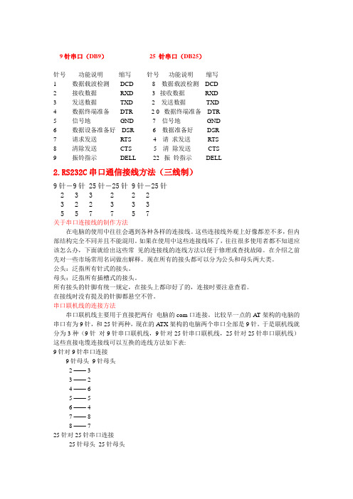
9针串口(DB9)25 针串口(DB25)针号功能说明缩写针号功能说明缩写1 数据载波检测DCD 8 数据载波检测DCD2 接收数据RXD3 接收数据RXD3 发送数据TXD 2 发送数据TXD4 数据终端准备DTR 2 0 数据终端准备DTR5 信号地 GND 7 信号地GND6 数据设备准备好DSR 6 数据准备好DSR7 请求发送RTS 4 请求发送RTS8 清除发送CTS 5 清除发送CTS9 振铃指示DELL 22 振铃指示 DELL2.RS232C串口通信接线方法(三线制)9针-9针 25针-25针 9针-25针2 3 3 2 2 23 2 2 3 3 35 5 7 7 5 7关于串口连接线的制作方法在电脑的使用中往往会遇到各种各样的连接线。
这些连接线外观上好像都差不多,但内部结构完全不同并且不能混用。
如果在使用中这些连接线坏了,往往很多使用者都不知道应该怎么办,下面就给出这些常见的连接线的连线方法以便于修理或查找故障。
在介绍之前先对一些市场常用名词做出解释。
现在所有的接头都可以分为公头和母头两大类。
公头:泛指所有针式的接头。
母头:泛指所有插槽式的接头。
所有接头的针脚有统一规定,在接头上都印好了的,连接时要注意查看。
在接线时没有提及的针脚都悬空不管。
串口联机线的连接方法串口联机线主要用于直接把两台电脑的com口连接。
比较早一点的AT架构的电脑的串口有为9针,和25针两种,现在的ATX架构的电脑两个串口全部是9针。
于是联机线就分为3种(9针对9针串口联机线,9针对25针串口联机线,25针对25针串口联机线)这些直接电缆连接线可以互换的连线方法如下表:9针对9针串口连接9针母头9针母头2 —— 33 —— 24 —— 65 —— 56 —— 47 —— 88 —— 725针对25针串口连接25针母头25针母头2 —— 33 —— 24 —— 55 —— 46 —— 207 —— 720 —— 69针对25针串口连接9针母头25针母头2 —— 23 —— 34 —— 65 —— 76 —— 207 —— 58 —— 4串口转接线这种转接线适用于9针串口和25针串口的转换。

串口通信的基本概念:1,什么是串口?2,什么是RS-232?3,什么是RS-422?4,什么是RS-485?5,什么是握手?1,什么是串口串口是计算机上一种非常通用设备通信的协议(不要与通用串行总线Universal Serial Bus或者USB混淆)。
大多数计算机包含两个基于RS232的串口。
串口同时也是仪器仪表设备通用的通信协议;很多GPIB兼容的设备也带有RS-232口。
同时,串口通信协议也可以用于获取远程采集设备的数据。
串口通信的概念非常简单,串口按位(bit)发送和接收字节。
尽管比按字节(byte)的并行通信慢,但是串口可以在使用一根线发送数据的同时用另一根线接收数据。
它很简单并且能够实现远距离通信。
比如IEEE488定义并行通行状态时,规定设备线总常不得超过20米,并且任意两个设备间的长度不得超过2米;而对于串口而言,长度可达1200米。
典型地,串口用于ASCII码字符的传输。
通信使用3根线完成:(1)地线,(2)发送,(3)接收。
由于串口通信是异步的,端口能够在一根线上发送数据同时在另一根线上接收数据。
其他线用于握手,但是不是必须的。
串口通信最重要的参数是波特率、数据位、停止位和奇偶校验。
对于两个进行通行的端口,这些参数必须匹配:a,波特率:这是一个衡量通信速度的参数。
它表示每秒钟传送的bit的个数。
例如300波特表示每秒钟发送300个bit。
当我们提到时钟周期时,我们就是指波特率例如如果协议需要4800波特率,那么时钟是4800Hz。
这意味着串口通信在数据线上的采样率为4800Hz。
通常电话线的波特率为14400,28800和36600。
波特率可以远远大于这些值,但是波特率和距离成反比。
高波特率常常用于放置的很近的仪器间的通信,典型的例子就是GPIB设备的通信。
b,数据位:这是衡量通信中实际数据位的参数。
当计算机发送一个信息包,实际的数据不会是8位的,标准的值是5、7和8位。
如何设置取决于你想传送的信息。