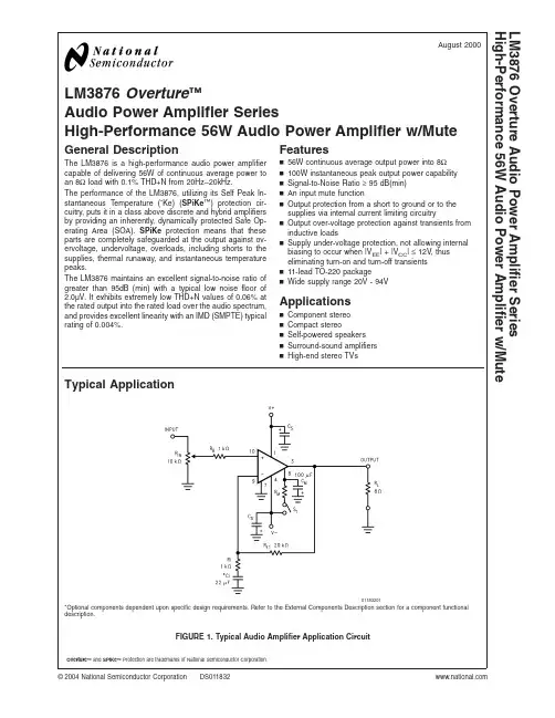
LM3876Overture ™Audio Power Amplifier SeriesHigh-Performance 56W Audio Power Amplifier w/MuteGeneral DescriptionThe LM3876is a high-performance audio power amplifier capable of delivering 56W of continuous average power to an 8Ωload with 0.1%THD+N from 20Hz–20kHz.The performance of the LM3876,utilizing its Self Peak In-stantaneous Temperature (˚Ke)(SPiKe ™)protection cir-cuitry,puts it in a class above discrete and hybrid amplifiers by providing an inherently,dynamically protected Safe Op-erating Area (SOA).SPiKe protection means that these parts are completely safeguarded at the output against ov-ervoltage,undervoltage,overloads,including shorts to the supplies,thermal runaway,and instantaneous temperature peaks.The LM3876maintains an excellent signal-to-noise ratio of greater than 95dB (min)with a typical low noise floor of 2.0µV.It exhibits extremely low THD+N values of 0.06%at the rated output into the rated load over the audio spectrum,and provides excellent linearity with an IMD (SMPTE)typical rating of 0.004%.Featuresn 56W continuous average output power into 8Ωn 100W instantaneous peak output power capability n Signal-to-Noise Ratio ≥95dB(min)n An input mute functionn Output protection from a short to ground or to the supplies via internal current limiting circuitryn Output over-voltage protection against transients from inductive loadsnSupply under-voltage protection,not allowing internal biasing to occur when |V EE |+|V CC |≤12V,thus eliminating turn-on and turn-off transients n 11-lead TO-220packagenWide supply range 20V -94VApplicationsn Component stereo n Compact stereon Self-powered speakers n Surround-sound amplifiers nHigh-end stereo TVsTypical ApplicationOverture ™and SPiKe ™Protection are trademarks of National Semiconductor Corporation.01183201*Optional components dependent upon specific design requirements.Refer to the External Components Description section for a component functional description.FIGURE 1.Typical Audio Amplifier Application CircuitAugust 2000LM3876Overture Audio Power Amplifier Series High-Performance 56W Audio Power Amplifier w/Mute©2004National Semiconductor Corporation Connection DiagramPlastic Package (Note 11)01183202†Connect Pin 5to V +for Compatibility with LM3886.Top View Order Number LM3876Tor LM3876TFSee NS Package Number TA11B forStaggered LeadNon-IsolatedPackage or TF11B forStaggered Lead Isolated PackageL M 3876 2Absolute Maximum Ratings(Notes4, 5)If Military/Aerospace specified devices are required, please contact the National Semiconductor Sales Office/ Distributors for availability and specifications.Supply Voltage|V+|+|V−|(No Signal)94V Supply Voltage|V+|+|V−|(Input Signal)84V Common Mode Input Voltage(V+or V−)and|V+|+|V−|≤80V Differential Input Voltage60V Output Current Internally Limited Power Dissipation(Note6)125W ESD Susceptibility(Note7)3000V Junction Temperature(Note8)150˚C Soldering InformationT Package(10seconds)260˚CStorage Temperature−40˚C to+150˚C Thermal ResistanceθJC1˚C/W θJA43˚C/W Operating Ratings(Notes4,5)Temperature RangeT MIN≤T A≤T MAX−20˚C≤T A≤+85˚C Supply Voltage|V+|+|V−|24V to84VNote1:Operation is guaranteed up to84V,however,distortion may be introduced from SPiKe Protection Circuitry when operating above70V if proper thermal considerations are not taken into account.Refer to the Thermal Considerations section for more information.(See SPiKe Protection Response)Electrical Characteristics(Notes4,5)The following specifications apply for V+=+35V,V−=−35V,I MUTE=−0.5mA with R L=8Ωunless otherwise specified.Limits apply for T A=25˚C.Symbol Parameter Conditions LM3876Units(Limits)Typical Limit(Note9)(Note10)|V+|+|V−|Power Supply Voltage(Note13)V pin7−V−≥9V1824V(min)84V(max) A M Mute Attenuation Pin8Open or at0V,Mute:OnCurrent out of Pin8>0.5mA,12080dB(min)Mute:OffP O(Note3)Output Power(Continuous Average)THD+N=0.1%(max)5640W(min)f=1kHz;f=20kHzPeak P O Instantaneous Peak Output Power100W THD+N Total Harmonic Distortion Plus Noise40W,20Hz≤f≤20kHz0.06%A V=26dBSR(Note3)Slew Rate(Note12)V IN=1.2Vrms,f=10kHz,115V/µs(min)Square-Wave,R L=2kΩI+(Note2)Total Quiescent Power Supply Current V CM=0V,V o=0V,I o=0A,I mute=0A3070mA(max) V OS(Note2)Input Offset Voltage V CM=0V,I o=0mA115mV(max) I B Input Bias Current V CM=0V,I o=0mA0.21µA(max) I OS Input Offset Current V CM=0V,I o=0mA0.010.2µA(max) I o Output Current Limit|V+|=|V−|=12V,t ON=10ms,V O=0V64A(min)V od (Note2)Output Dropout Voltage(Note14)|V+–V O|,V+=20V,I o=+100mA 1.65V(max)|V O–V−|,V−=−20V,I o=−100mA 2.75V(max)PSRR (Note2)Power Supply Rejection Ratio V+=40V to20V,V−=−40V,12085dB(min)V CM=0V,I o=0mAV+=40V,V−=−40V to−20V,12085dB(min)V CM=0V,I o=0mACMRR (Note2)Common Mode Rejection Ratio V+=60V to20V,V−=−20V to−60V,12080dB(min)V CM=20V to−20V,I o=0mAA VOL (Note2)Open Loop Voltage Gain|V+|=|V−|=40V,R L=2kΩ,∆V O=60V12090dB(min)LM38763Electrical Characteristics (Notes 4,5)(Continued)The following specifications apply for V +=+35V,V −=−35V,I MUTE =−0.5mA with R L =8Ωunless otherwise specified.Limits apply for T A =25˚C.SymbolParameterConditionsLM3876Units (Limits)Typical Limit (Note 9)(Note 10)GBWP Gain-Bandwidth Product |V +|=|V −|=40V82MHz (min)f O =100kHz,V IN =50mVrms e IN (Note 3)Input Noise IHF —A Weighting Filter 2.08µV (max)R IN =600Ω(Input Referred)SNRSignal-to-Noise RatioP O =1W,A-Weighted,98dB Measured at 1kHz,R S =25ΩP O =40W,A-Weighted,114dB Measured at 1kHz,R S =25ΩPpk=100W,A-Weighted,122dB Measured at 1kHz,R S =25ΩIMD Intermodulation Distortion Test 60Hz,7kHz,4:1(SMPTE)0.004%60Hz,7kHz,1:1(SMPTE)0.006Note 2:DC Electrical Test;refer to Test Circuit #1.Note 3:AC Electrical Test;refer to Test Circuit #2.Note 4:All voltages are measured with respect to the GND pin (pin 7),unless otherwise specified.Note 5:Absolute Maximum Ratings indicate limits beyond which damage to the device may occur.Operating Ratings indicate conditions for which the device is functional,but do not guarantee specific performance limits.Electrical Characteristics state DC and AC electrical specifications under particular test conditions which guarantee specific performance limits.This assumes that the device is within the Operating Ratings.Specifications are not guaranteed for parameters where no limit is given,however,the typical value is a good indication of device performance.Note 6:For operating at case temperatures above 25˚C,the device must be derated based on a 150˚C maximum junction temperature and a thermal resistance of θJC =1.0˚C/W (junction to case).Refer to the Thermal Resistance figure in the Application Information section under Thermal Considerations.Note 7:Human body model,100pF discharged through a 1.5k Ωresistor.Note 8:The operating junction temperature maximum is 150˚C,however,the instantaneous Safe Operating Area temperature is 250˚C.Note 9:Typicals are measured at 25˚C and represent the parametric norm.Note 10:Limits are guaranteed to National’s AOQL (Average Outgoing Quality Level).Note 11:The LM3876T package TA11B is a non-isolated package,setting the tab of the device and the heat sink at V −potential when the LM3876is directly mounted to the heat sink using only thermal compound.If a mica washer is used in addition to thermal compound,θCS (case to sink)is increased,but the heat sink will be isolated from V −.Note 12:The feedback compensation network limits the bandwidth of the closed-loop response and so the slew rate will be reduced due to the high frequency roll-off.Without feedback compensation,the slew rate is typically 16V/µs.Note 13:V −must have at least −9V at its pin with reference to ground in order for the under-voltage protection circuitry to be disabled.Note 14:The output dropout voltage is the supply voltage minus the clipping voltage.Refer to the Clipping Voltage vs Supply Voltage graph in the Typical Performance Characteristics section.L M 3876 4Test Circuit #1(DC Electrical Test Circuit)01183203Test Circuit #2(AC Electrical Test Circuit)01183204LM38765Single Supply Application Circuit01183205*Optional components dependent upon specific design requirements.Refer to the External Components Description section for a component functional description.FIGURE 2.Typical Single Supply Audio Amplifier Application CircuitL M 3876 6LM3876 Equivalent Schematic(excluding active protection circuitry)7External Components Description(Figures 1,2)Components Functional Description1.R IN Acts as a volume control by setting the voltage level allowed to the amplifier’s input terminals.2.R A Provides DC voltage biasing for the single supply operation and bias current for the positive input terminal.3.C A Provides bias filtering.4.C Provides AC coupling at the input and output of the amplifier for single supply operation.5.R BPrevents currents from entering the amplifier’s non-inverting input which may be passed through to the load upon power-down of the system due to the low input impedance of the circuitry when the under-voltage circuitry is off.This phenomenon occurs when the supply voltages are below 1.5V.6.C C(Note 15)Reduces the gain (bandwidth of the amplifier)at high frequencies to avoid quasi-saturation oscillations of the output transistor.The capacitor also suppresses external electromagnetic switching noise created from fluorescent lamps.7.Ri Inverting input resistance to provide AC Gain in conjunction with R f1.8.Ci(Note 15)Feedback capacitor.Ensures unity gain at DC.Also a low frequency pole (highpass roll-off)at:f c =1/(2πRi Ci)9.R f1Feedback resistance to provide AC Gain in conjunction with Ri.10.R f2(Note 15)At higher frequencies feedback resistance works with C f to provide lower AC Gain in conjunction with R f1and Ri.A high frequency pole (lowpass roll-off)exists at:f c =[R f1R f2(s +1/R f2C f )]/[(R f1+R f2)(s +1/C f (R f1+R f2))]11.C f(Note 15)Compensation capacitor that works with R f1and R f2to reduce the AC Gain at higher frequencies.12.R MMute resistance set up to allow 0.5mA to be drawn from pin 8to turn the muting function off.→R M is calculated using:R M ≤(|V EE |−2.6V)/I8where I8≥0.5mA.Refer to the Mute Attenuation vs Mute Current curves in the Typical Performance Characteristics section.13.C MMute capacitance set up to create a large time constant for turn-on and turn-off muting.14.R SN(Note 15)Works with C SN to stabilize the output stage by creating a pole that eliminates high frequency oscillations.15.C SN(Note 15)Works with R SN to stabilize the output stage by creating a pole that eliminates high frequency oscillations.f c =1/(2πR SN C SN )16.L(Note 15)Provides high impedance at high frequecies so that R may decouple a highly capacitive load17.R(Note 15)and reduce the Q of the series resonant circuit due to capacitive load.Also provides a low impedance at low frequencies to short out R and pass audio signals to the load.18.C S Provides power supply filtering and bypassing.19.S1Mute switch that mutes the music going into the amplifier when opened.Note 15:Optional components dependent upon specific design requirements.Refer to the Application Information section for more information.OPTIONAL EXTERNAL COMPONENT INTERACTION Although the optional external components have specific desired functions that are designed to reduce the bandwidth and eliminate unwanted high frequency oscillations they may cause certain undesirable effects when they interact.Inter-action may occur for components whose reactances are in close proximity to one another.One example would be the coupling capacitor,C C ,and the compensation capacitor,Cf.These two components act as low impedances to certain frequencies which will couple signals from the input to the output.Please take careful note of basic amplifier compo-nent functionality when designing in these components.The optional external components shown in Figure 2and described above are applicable in both single and split volt-age supply configurations.L M 3876 8Typical Performance CharacteristicsSafe AreaSPiKeProtection Response 0118321701183218Supply Current vs Supply VoltagePulse ThermalResistance0118321901183220Pulse Thermal ResistanceSupply Current vsOutput Voltage0118322101183222LM3876 9Typical Performance Characteristics(Continued)Pulse Power LimitPulse Power Limit0118322301183224Supply Current vs Case TemperaturePulse Response0118322501183226Input Bias Current vs Case Temperature Clipping Voltage vs Supply Voltage0118322701183228L M 3876 10Typical Performance Characteristics(Continued)THD+N vs Frequency THD+N vs Output Power0118322901183230 THD+N vs Output Power THD+N Distribution0118323101183232THD+N DistributionOutput Power vsLoad Resistance0118323301183234LM3876 11Typical Performance Characteristics(Continued)Max Heatsink Thermal Resistance (˚C/W)at the Specified Ambient Temperature (˚C)PDmax r vs Supply Voltage01183209Note:The maximum heat sink thermal resistance values,øSA ,in the table above were calculated using a øCS =0.2˚C/W due to thermal compoundPower Dissipation vsOutput Power Power Dissipation vsOutput Power0118323501183236Output Power vs Supply VoltageIMD 60Hz,4:10118323701183238L M 3876 12Typical Performance Characteristics(Continued)IMD60Hz,7kHz,4:1IMD60Hz,7kHz,4:10118323901183240 IMD60Hz,1:1IMD60Hz,7kHz1:10118324101183242IMD60Hz,7kHz,1:1Mute Attenuation vsMute Current0118324301183244LM3876 13Typical Performance Characteristics(Continued)Mute Attenuation vsMute CurrentLarge Signal Response0118324501183246Power Supply Rejection Ratio Common-Mode Rejection Ratio0118324701183248Open LoopFrequency Response01183249L M 3876 14Application InformationGENERAL FEATURESMute Function:The muting function of the LM3876allows the user to mute the music going into the amplifier by draw-ing less than0.5mA out of pin8of the device.This is accomplished as shown in the Typical Application Circuit where the resistor R M is chosen with reference to your negative supply voltage and is used in conjuction with a switch.The switch(when opened)cuts off the current flow from pin8to V−,thus placing the LM3876into mute mode. Refer to the Mute Attenuation vs Mute Current curves in the Typical Performance Characteristics section for values of attenuation per current out of pin8.The resistance R M is calculated by the following equation:R M(|V EE|−2.6V)/I8where I8≥0.5mA.Under-Voltage Protection:Upon system power-up the under-voltage protection circuitry allows the power supplies and their corresponding caps to come up close to their full values before turning on the LM3876such that no DC output spikes occur.Upon turn-off,the output of the LM3876is brought to ground before the power supplies such that no transients occur at power-down.Over-Voltage Protection:The LM3876contains overvolt-age protection circuitry that limits the output current to ap-proximately6Apeak while also providing voltage clamping, though not through internal clamping diodes.The clamping effect is quite the same,however,the output transistors are designed to work alternately by sinking large current spikes. SPiKe Protection:The LM3876is protected from instanta-neous peak-temperature stressing by the power transistor array.The Safe Operating Area graph in the Typical Perfor-mance Characteristics section shows the area of device operation where the SPiKe Protection Circuitry is not en-abled.The waveform to the right of the SOA graph exempli-fies how the dynamic protection will cause waveform distor-tion when enabled.Thermal Protection:The LM3876has a sophisticated ther-mal protection scheme to prevent long-term thermal stress to the device.When the temperature on the die reaches 165˚C,the LM3876shuts down.It starts operating again when the die temperature drops to about155˚C,but if the temperature again begins to rise,shutdown will occur again at165˚C.Therefore the device is allowed to heat up to a relatively high temperature if the fault condition is temporary, but a sustained fault will cause the device to cycle in a Schmitt Trigger fashion between the thermal shutdown tem-perature limits of165˚C and155˚C.This greatly reduces the stress imposed on the IC by thermal cycling,which in turn improves its reliability under sustained fault conditions. Since the die temperature is directly dependent upon the heat sink,the heat sink should be chosen as discussed in the Thermal Considerations section,such that thermal shutdown will not be reached during normal ing the best heat sink possible within the cost and space con-straints of the system will improve the long-term reliability of any power semiconductor device.THERMAL CONSIDERATIONSHeat SinkingThe choice of a heat sink for a high-power audio amplifier is made entirely to keep the die temperature at a level such that the thermal protection circuitry does not operate undernormal circumstances.The heat sink should be chosen todissipate the maximum IC power for a given supply voltageand rated load.With high-power pulses of longer duration than100ms,thecase temperature will heat up drastically without the use of aheat sink.Therefore the case temperature,as measured atthe center of the package bottom,is entirely dependent onheat sink design and the mounting of the IC to the heat sink.For the design of a heat sink for your audio amplifier appli-cation refer to the Determining The Correct Heat Sinksection.Since a semiconductor manufacturer has no control overwhich heat sink is used in a particular amplifier design,wecan only inform the system designer of the parameters andthe method needed in the determination of a heat sink.Withthis in mind,the system designer must choose his supplyvoltages,a rated load,a desired output power level,andknow the ambient temperature surrounding the device.These parameters are in addition to knowing the maximumjunction temperature and the thermal resistance of the IC,both of which are provided by National Semiconductor.As a benefit to the system designer we have provided Maxi-mum Power Dissipation vs Supply Voltages curves for vari-ous loads in the Typical Performance Characteristics sec-tion,giving an accurate figure for the maximum thermalresistance required for a particular amplifier design.Thisdata was based onθJC=1˚C/W andθCS=0.2˚C/W.We alsoprovide a section regarding heat sink determination for anyaudio amplifier design whereθCS may be a different value.Itshould be noted that the idea behind dissipating the maxi-mum power within the IC is to provide the device with a lowresistance to convection heat transfer such as a heat sink.Therefore,it is necessary for the system designer to beconservative in his heat sink calculations.As a rule,thelower the thermal resistance of the heat sink the higher theamount of power that may be dissipated.This is of courseguided by the cost and size requirements of the system.Convection cooling heat sinks are available commercially,and their manufacturers should be consulted for ratings.Proper mounting of the IC is required to minimize the thermaldrop between the package and the heat sink.The heat sinkmust also have enough metal under the package to conductheat from the center of the package bottom to the finswithout excessive temperature drop.A thermal grease such as Wakefield type120or ThermalloyThermacote should be used when mounting the package tothe heat sink.Without this compound,thermal resistance willbe no better than0.5˚C/W,and probably much worse.Withthe compound,thermal resistance will be0.2˚C/W or less,assuming under0.005inch combined flatness runout for thepackage and heat sink.Proper torquing of the mountingbolts is important and can be determined from heat sinkmanufacturer’s specification sheets.Should it be necessary to isolate V−from the heat sink,aninsulating washer is required.Hard washers like beryluumoxide,anodized aluminum and mica require the use of ther-mal compound on both faces.Two-mil mica washers aremost common,giving about0.4˚C/W interface resistancewith the compound.Silicone-rubber washers are also available.A0.5˚C/W ther-mal resistance is claimed without thermal compound.Expe-rience has shown that these rubber washers deteriorate andmust be replaced should the IC be dismounted.LM387615Application Information(Continued)Determining Maximum Power DissipationPower dissipation within the integrated circuit package is a very important parameter requiring a thorough understand-ing if optimum power output is to be obtained.An incorrect maximum power dissipation (P D )calculation may result in inadequate heat sinking,causing thermal shutdown circuitry to operate and limit the output power.The following equations can be used to acccurately calculate the maximum and average integrated circuit power dissipa-tion for your amplifier design,given the supply voltage,rated load,and output power.These equations can be directly applied to the Power Dissipation vs Output Power curves in the Typical Performance Characteristics section.Equation (1)exemplifies the maximum power dissipation of the IC and Equations (2),(3)exemplify the average IC power dissipation expressed in different forms.P DMAX =V CC 2/2π2R L(1)where V CC is the total supply voltageP DAVE =(V Opk /R L )[V CC /π−V Opk /2](2)where V CC is the total supply voltage and V Opk =V CC /πP DAVE =V CC V Opk /πR L −V Opk 2/2R L(3)where V CC is the total supply voltage.Determining the Correct Heat SinkOnce the maximum IC power dissipation is known for a given supply voltage,rated load,and the desired rated out-put power the maximum thermal resistance (in ˚C/W)of a heat sink can be calculated.This calculation is made using Equation (4)and is based on the fact that thermal heat flow parameters are analogous to electrical current flow proper-ties.It is also known that typically the thermal resistance,θJC (junction to case),of the LM3876is 1˚C/W and that using Thermalloy Thermacote thermal compound provides a ther-mal resistance,θCS (case to heat sink),of about 0.2˚C/W as explained in the Heat Sinking section.Referring to the figure below,it is seen that the thermal resistance from the die (junction)to the outside air (ambient)is a combination of three thermal resistances,two of which are known,θJC and θCS .Since convection heat flow (power dissipation)is analogous to current flow,thermal resistance is analogous to electrical resistance,and temperature drops are analogous to voltage drops,the power dissipation out of the LM3876is equal to the following:P DMAX =(T Jmax −T Amb )/θJAwhere θJA =θJC +θCS +θSA01183212But since we know P DMAX ,θJC ,and θSC for the application and we are looking for θSA ,we have the following:θSA =[(T Jmax −T Amb )−P DMAX (θJC +θCS )]/P DMAX (4)Again it must be noted that the value of θSA is dependent upon the system designer’s amplifier application and its corresponding parameters as described previously.If the ambient temperature that the audio amplifier is to be workingunder is higher than the normal 25˚C,then the thermal resistance for the heat sink,given all other things are equal,will need to be smaller.Equations (1),(4)are the only equations needed in the determination of the maximum heat sink thermal resistance.This is of course given that the system designer knows the required supply voltages to drive his rated load at a particular power output level and the parameters provided by the semiconductor manufacturer.These parameters are the junction to case thermal resistance,θJC ,T Jmax =150˚C,and the recommended Thermalloy Thermacote thermal com-pound resistance,θCS .SIGNAL-TO-NOISE RATIOIn the measurement of the signal-to-noise ratio,misinterpre-tations of the numbers actually measured are common.One amplifier may sound much quieter than another,but due to improper testing techniques,they appear equal in measure-ments.This is often the case when comparing integrated circuit designs to discrete amplifier designs.Discrete transis-tor amps often “run out of gain”at high frequencies and therefore have small bandwidths to noise as indicated below.01183213Integrated circuits have additional open loop gain allowing additional feedback loop gain in order to lower harmonic distortion and improve frequency response.It is this addi-tional bandwidth that can lead to erroneous signal-to-noise measurements if not considered during the measurement process.In the typical example above,the difference in bandwidth appears small on a log scale but the factor of 10in bandwidth,(200kHz to 2MHz)can result in a 10dB theoretical difference in the signal-to-noise ratio (white noise is proportional to the square root of the bandwidth in a system).In comparing audio amplifiers it is necessary to measure the magnitude of noise in the audible bandwidth by using a “weighting”filter (Note 16).A “weighting”filter alters the frequency response in order to compensate for the average human ear’s sensitivity to the frequency spectra.The weight-ing filters at the same time provide the bandwidth limiting as discussed in the previous paragraph.Note 16:CCIR/ARM:A Practical Noise Measurement Method;by Ray Dolby,David Robinson and Kenneth Gundry,AES Preprint No.1353(F-3).In addition to noise filtering,differing meter types give differ-ent noise readings.Meter responses include:1.RMS reading,2.average responding,3.peak reading,and4.quasi peak reading.Although theoretical noise analysis is derived using true RMS based calculations,most actual measurements are taken with ARM (Average Responding Meter)test equip-ment.L M 387616Application Information(Continued)Typical signal-to-noise figures are listed for an A-weighted filter which is commonly used in the measurement of noise.The shape of all weighting filters is similar,with the peak of the curve usually occurring in the 3kHz–7kHz region as shown below.01183214SUPPLY BYPASSINGThe LM3876has excellent power supply rejection and does not require a regulated supply.However,to eliminate pos-sible oscillations all op amps and power op amps should have their supply leads bypassed with low-inductance ca-pacitors having short leads and located close to the package terminals.Inadequate power supply bypassing will manifest itself by a low frequency oscillation known as “motorboating”or by high frequency instabilities.These instabilities can be eliminated through multiple bypassing utilizing a large tanta-lum or electrolytic capacitor (10µF or larger)which is used to absorb low frequency variations and a small ceramic capaci-tor (0.1µF)to prevent any high frequency feedback through the power supply lines.If adequate bypassing is not provided the current in the supply leads which is a rectified component of the load current may be fed back into internal circuitry.This signal causes low distortion at high frequencies requiring that the supplies be bypassed at the package terminals with an electrolytic capacitor of 470µF or more.LEAD INDUCTANCEPower op amps are sensitive to inductance in the output lead,particularly with heavy capacitive loading.Feedback to the input should be taken directly from the output terminal,minimizing common inductance with the load.Lead inductance can also cause voltage surges on the sup-plies.With long leads to the power supply,energy is stored in the lead inductance when the output is shorted.This energy can be dumped back into the supply bypass capacitors when the short is removed.The magnitude of this transient is reduced by increasing the size of the bypass capacitor near the IC.With at least a 20µF local bypass,these voltage surges are important only if the lead length exceeds a couple feet (>1µH lead inductance).Twisting together the supply and ground leads minimizes the effect.LAYOUT,GROUND LOOPS AND STABILITYThe LM3876is designed to be stable when operated at a closed-loop gain of 10or greater,but as with any other high-current amplifier,the LM3876can be made to oscillate under certain conditions.These usually involve printed cir-cuit board layout or output/input coupling.When designing a layout,it is important to return the load ground,the output compensation ground,and the low level(feedback and input)grounds to the circuit board common ground point through separate paths.Otherwise,large cur-rents flowing along a ground conductor will generate volt-ages on the conductor which can effectively act as signals at the input,resulting in high frequency oscillation or excessive distortion.It is advisable to keep the output compensation components and the 0.1µF supply decoupling capacitors as close as possible to the LM3876to reduce the effects of PCB trace resistance and inductance.For the same reason,the ground return paths should be as short as possible.In general,with fast,high-current circuitry,all sorts of prob-lems can arise from improper grounding which again can be avoided by returning all grounds separately to a common point.Without isolating the ground signals and returning the grounds to a common point,ground loops may occur.“Ground Loop”is the term used to describe situations occur-ring in ground systems where a difference in potential exists between two ground points.Ideally a ground is a ground,but unfortunately,in order for this to be true,ground conductors with zero resistance are necessary.Since real world ground leads possess finite resistance,currents running through them will cause finite voltage drops to exist.If two ground return lines tie into the same path at different points there will be a voltage drop between them.The first figure below shows a common ground example where the positive input ground and the load ground are returned to the supply ground point via the same wire.The addition of the finite wire resistance,R 2,results in a voltage difference between the two points as shown below.01183215The load current I L will be much larger than input bias current I I ,thus V 1will follow the output voltage directly,i.e.in phase.Therefore the voltage appearing at the non-inverting input is effectively positive feedback and the circuit may oscillate.If there were only one device to worry about then the values of R 1and R 2would probably be small enough to be ignored;however,several devices normally comprise a total system.Any ground return of a separate device,whose output is inLM387617。