pcb焊盘设计大全
- 格式:pdf
- 大小:93.24 KB
- 文档页数:22
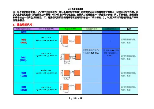
注:以下设计标准参照了IPC-SM-782A标准和一些日本著名设计制造厂家的设计以及在制造经验中积累的一些较好的设计方案。
以供大家参考和使用(焊盘设计总体思想:CHIP件当中尺寸标准的,按照尺寸规格给出一个焊盘设计标准;尺寸不标准的,按照其物料编号给出一个焊盘设计标准。
IC、连接器元件按照物料编号或规格归类给出一个设计标准。
),以减少设计问题给实际生产带来的诸多困扰。
1、焊盘规范尺寸:规格(或物料编号) 物料具体参数(mm) 焊盘设计(mm) 印锡钢网设计印胶钢网设计备注01005 / / / /0201 (0603)a=0.10±0.05b=0.30±0.05,c=0.60±0.05 /适用及普通电阻、电容、电感0402 (1005)a=0.20±0.10b=0.50±0.10,c=1.00±0.10以焊盘中心为中心,开孔圆形D=0.55mm开口宽度0.2mm(钢网厚度T建议厚度为0.15mm)适用及普通电阻、电容、电感0603 (1608)a=0.30±0.20,b=0.80±0.15,c=1.60±0.15 适用及普通电阻、电容、电感0805 (2012)a=0.40±0.20b=1.25±0.15,c=2.00±0.20适用及普通电阻、电容、电感1 / 251 / 251206 (3216)a=0.50±0.20b=1.60±0.15,c=3.20±0.20适用及普通电阻、电容、电感1210 (3225)a=0.50±0.20b=2.50±0.20,c=3.20±0.20适用及普通电阻、电容、电感1812 (4532)a=0.50±0.20b=3.20±0.20,c=4.50±0.20适用及普通电阻、电容、电感2010 (5025)a=0.60±0.20b=2.50±0.20,c=5.00±0.20适用及普通电阻、电容、电感2512 (6432)a=0.60±0.20b=3.20±0.20,c=6.40±0.20适用及普通电阻、电容、电感5700-250AA2-03001:1开口,不避锡珠2 / 252 / 25排阻0404(1010)a=0.25±0.10,b=1.00±0.10c=1.00±0.10,d=0.35±0.10p=0.65±0.05排阻0804 (2010)a=0.25±0.10,b=2.00±0.10 c=1.00±0.10,d=0.30±0.15p=0.50±0.05排阻1206(3216)a=0.30±0.15,b=3.2±0.15c=1.60±0.15,d=0.50±0.15p=0.80±0.10排阻1606(4016)a=0.25±0.10,b=4.00±0.20c=1.60±0.15,d=0.30±0.103 / 253 / 254 / 254 / 25p=0.50±0.05472X-R05240-10a=0.38±0.05,b=2.50±0.10 c=1.00±0.10,d=0.20±0.05d1=0.40±0.05,p=0.50钽质电容适用于钽质电容1206 (3216) a=0.80±0.30,b=1.60±0.20 c=3.20±0.20,d=1.20±0.10 A=1.50,B=1.20,G=1.401411 (3528) a=0.80±0.30,b=2.80±0.20 c=3.50±0.20,d=2.20±0.10 A=1.50,B=2.20,G=1.702312 (6032) a=1.30±0.30,b=3.20±0.30 c=6.00±0.30,d=2.20±0.10 A=2.00,B=2.20,G=3.202917 (7243)a=1.30±0.30,b=4.30±0.30 c=7.20±0.30,d=2.40±0.10A=2.00,B=2.40,G=4.50铝质 电解 电容适用于铝质电解电容(Ø4×5.4)d=4.0±0.5a=1.8±0.2,b=4.3±0.2 c=4.3±0.2,e=0.5~0.8A=2.40,B=1.00 P=1.20,R=0.50h=5.4±0.3p=1.0(Ø5×5.4) d=5.0±0.5 h=5.4±0.3a=2.2±0.2,b=5.3±0.2c=5.3±0.2,e=0.5~0.8p=1.3A=2.80,B=1.00P=1.50,R=0.50(Ø6.3×5.4) d=6.3±0.5 h=5.4±0.3a=2.6±0.2,b=6.6±0.2c=6.6±0.2,e=0.5~0.8p=2.2A=3.20,B=1.00P=2.40,R=0.50(Ø6.3×7.7) d=6.3±0.5 h=7.7±0.3a=2.6±0.2,b=6.6±0.2c=6.6±0.2,e=0.5~0.8p=2.2A=3.20,B=1.00P=2.40,R=0.50(Ø8.0×6.5) d=6.3±0.5 h=7.7±0.3a=3.0±0.2,b=8.3±0.2c=8.3±0.2,e=0.5~0.8p=2.2A=3.20,B=1.00P=2.40,R=0.50(Ø8×10.5) d=8.0±0.5 h=10.5±0.3a=3.0±0.2,b=8.3±0.2c=8.3±0.2,e=0.8~1.1p=3.1A=3.60,B=1.30P=3.30,R=0.65(Ø10×10.5) d=10.0±0.5 h=10.5±0.3a=3.5±0.2,b=10.3±0.2c=10.3±0.2,e=0.8~1.1p=4.6A=4.20,B=1.30P=4.80,R=0.65二极管(SMA)4500-234031-T04500-205100-T0a=1.20±0.30b=2.60±0.30,c=4.30±0.30d=1.45±0.20,e=5.2±0.305 / 255 / 25二极管(SOD-323)4500-141482-T0a=0.30±0.10b=1.30±0.10,c=1.70±0.10d=0.30±0.05,e=2.50±0.20二极管(3515)a=0.30b=1.50±0.1,c=3.50±0.20二极管(5025)a=0.55b=2.50±0.10, c=5.00±0.20三极管(SOT-523)a=0.40±0.10,b=0.80±0.05c=1.60±0.10,d=0.25±0.056 / 256 / 25p=1.00三极管(SOT-23)a=0.55±0.15,b=1.30±0.10c=2.90±0.10,d=0.40±0.10p=1.90±0.10SOT-25a=0.60±0.20,b=2.90±0.20c=1.60±0.20,d=0.45±0.10p=1.90±0.10SOT-26a=0.60±0.20,b=2.90±0.207 / 257 / 25c=1.60±0.20,d=0.45±0.10p=0.95±0.05SOT-223a1=1.75±0.25,a2=1.5±0.25b=6.50±0.20,c=3.50±0.20d1=0.70±0.1,d2=3.00±0.1p=2.30±0.05SOT-89a1=1.0±0.20,a2=0.6±0.20b=2.50±0.20,c=4.50±0.20d1=0.4±0.10,d2=0.5±0.10d3=1.65±0.20,p=1.5±0.058 / 258 / 25TO-252a1=1.1±0.2,a2=0.9±0.1b=6.6±0.20,c=6.1±0.20d1=5.0±0.2,d2=Max1.0e=9.70±0.70,p=2.30±0.10TO-263-2a1=1.30±0.1,a2=2.55±0.25b=9.97±0.32,c=9.15±0.50d1=1.3±0.10,d2=0.75±0.24e=15.25±0.50,p=2.54±0.109 / 259 / 25TO-263-3a1=1.30±0.1,a2=2.55±0.25b=9.97±0.32,c=9.15±0.50d1=1.3±0.10,d2=0.75±0.24e=15.25±0.50,p=2.54±0.10TO-263-5a1=1.66±0.1,a2=2.54±0.20b=10.03±0.15,c=8.40±0.20d=0.81±0.10,e=15.34±0.2p=1.70±0.1010 / 2510 / 25SOP(引脚(Pitch>0.65mm)A=a+1.0,B=d+0.1G=e-2*(0.4+a)P=pSOP(Pitch≦0.65mm)A=a+0.7,B=dG=e-2*(0.4+a)P=p11 / 2511 / 25SOJ(Pitch≧0.8mm)A=1.8mm,B=d2+0.10mmG=g-1.0mm,P=pQFP(Pitch≧0.65mm)A=a+1.0,B=d+0.05P=pG1=e1-2*(0.4+a)G2=e2-2*(0.4+a)12 / 2512 / 25QFP(Pitch=0.5mm)A=a+0.9,B=0.25mmP=pG1=e1-2*(0.4+a)G2=e2-2*(0.4+a)QFP(Pitch=0.4mm)A=a+0.8,B=0.19mmP=pG1=e1-2*(0.4+a)G2=e2-2*(0.4+a) 引脚长由原来的a+0.70mm更改为a+0.80mm,有利于修理和印刷拉尖的处理。
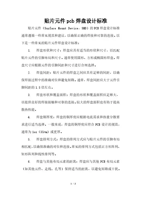
贴片元件pcb焊盘设计标准贴片元件(Surface Mount Device,SMD)的PCB焊盘设计标准通常遵循一些常见规范和建议,以确保正确的焊接和可靠的连接。
以下是一些常见的贴片元件焊盘设计标准:
1. 焊盘形状和尺寸:焊盘应具有适当的形状和尺寸,以匹配贴片元件的引脚布局和尺寸。
通常使用圆形、方形或椭圆形焊盘。
焊盘尺寸应根据元件的引脚间距和尺寸进行合理选择。
2. 焊盘间距:贴片元件的焊盘之间应具有足够的间距,以确保焊接过程中的准确对位和避免短路。
通常,焊盘间距应大于元件引脚间距的1.5倍左右。
3. 焊盘形状和覆盖面积:焊盘的形状和覆盖面积应足够大,以提供良好的焊接接触和可靠的连接。
较大的焊盘面积也有助于提高散热性能。
4. 焊盘铜厚度:焊盘的铜厚度应根据电流需求和热量分散要求进行适当选择。
一般来说,焊盘的铜厚度应符合PCB设计的规范,通常为1oz(35µm)或更厚。
5. 焊盘排列方式:焊盘的排列方式应与贴片元件的引脚布局相匹配,以确保准确的对位和连接。
常见的排列方式包括正方形阵列、矩形阵列和线性排列等。
6. 焊盘与其他布局元素的距离:焊盘应与其他PCB布局元素(如其他元件、走线、孔等)保持适当的距离,以避免短路或干扰。
1/ 2
7. 焊盘覆盖层:焊盘上可以添加焊盘覆盖层(Solder Mask)来防止短路和腐蚀。
焊盘覆盖层应正确设计和应用,以避免覆盖焊盘的必要接触区域。
这些是常见的贴片元件焊盘设计标准,但具体的设计要求可能会因制造商、元件类型和应用领域的不同而有所变化。
2/ 2。
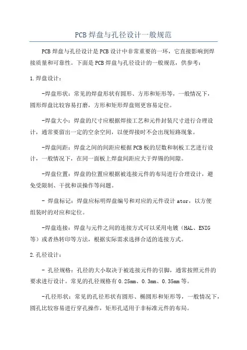
PCB焊盘与孔径设计一般规范PCB焊盘与孔径设计是PCB设计中非常重要的一环,它直接影响到焊接质量和可靠性。
下面是PCB焊盘与孔径设计的一般规范,供参考:1.焊盘设计:-焊盘形状:常见的焊盘形状有圆形、方形和矩形等,一般情况下,圆形焊盘比较容易打磨,方形和矩形焊盘则更容易定位。
-焊盘大小:焊盘的尺寸应根据焊接工艺和元件封装尺寸进行合理设计,通常要留出一定的空余空间,以便焊接时不会出现短路现象。
-焊盘间距:焊盘之间的间距应根据PCB板的层数和制板工艺进行设计,一般情况下,在同一面板上焊盘间距应大于焊锡的间隙。
-焊盘位置:焊盘的位置应根据被连接元件的布局进行合理设计,避免受限制、干扰和误操作等问题。
- 焊盘标记:焊盘应标明焊盘编号和对应的元件设计ator,以方便组装时的对应和定位。
-焊盘连接:焊盘与元件之间的连接方式可以采用电镀(HAL、ENIG等)或者热转印等方法,根据实际需求选择合适的连接方式。
2.孔径设计:- 孔径规格:孔径的大小取决于被连接元件的引脚,通常按照元件的要求进行设计。
常见的孔径规格有0.25mm、0.3mm、0.35mm等。
-孔径形状:常见的孔径形状有圆形、椭圆形和矩形等,一般情况下,圆孔比较容易进行穿孔操作,矩形孔适用于非标准元件的布局。
-孔径间距:孔径之间的间距应根据PCB板的层数和制板工艺进行设计,一般情况下,孔径间距应大于孔径的直径。
-孔径位置:孔径的位置应根据被连接元件的布局进行合理设计,避免受限制、干扰和误操作等问题。
- 孔径划线:孔径应标明孔径编号和对应的元件设计ator,以方便组装时的对应和定位。
-孔径填充:如果没有被连接元件需要通过孔径连接的话,可以考虑在孔径上进行焊盘填充,以增加板的机械强度。
总的来说,焊盘与孔径的设计需要考虑到焊接工艺、元件布局、层数和制板工艺等因素,合理设计可以提高焊接质量和可靠性。
每个项目都有其特定的需求,因此在实际设计前最好与组装、制板等相关人员进行沟通与确认。
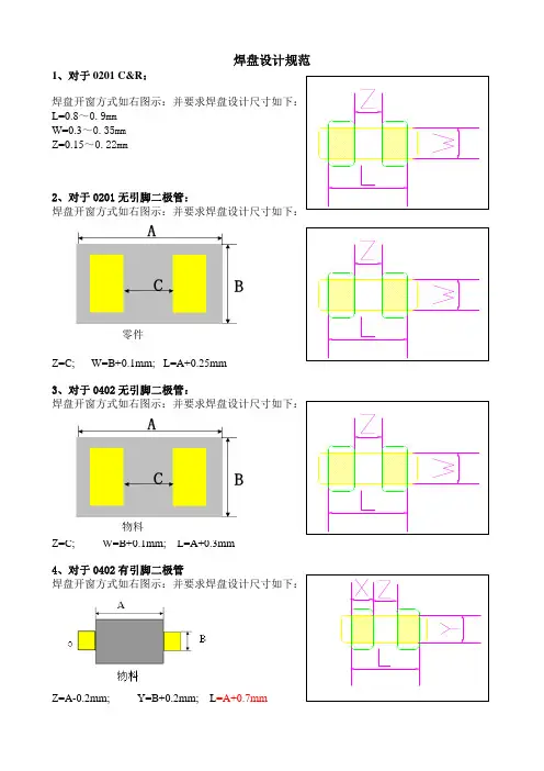
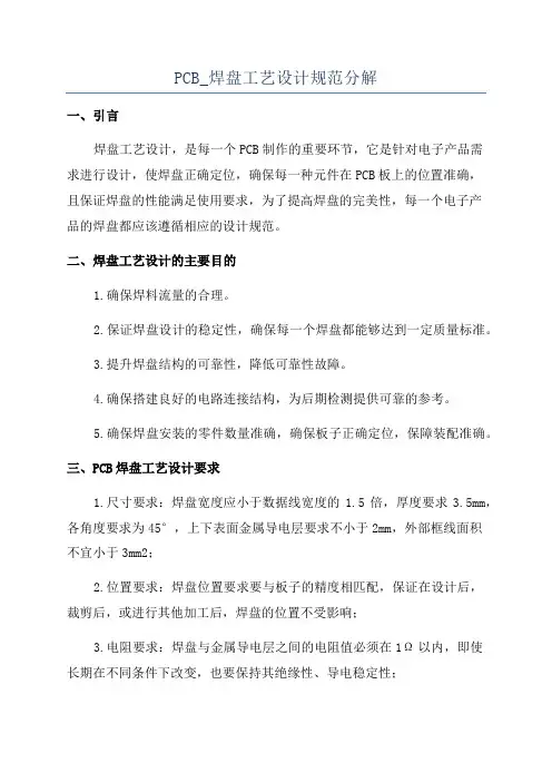
焊盘设计规范1、对于0201 C&R :焊盘开窗方式如右图示:并要求焊盘设计尺寸如下:L=0.8~0.9mmW=0.3~0.35mmZ=0.15~0.22mm2、对于0201无引脚二极管:焊盘开窗方式如右图示:并要求焊盘设计尺寸如下:Z=C; W=B+0.1mm; L=A+0.25mm3、对于0402无引脚二极管:焊盘开窗方式如右图示:并要求焊盘设计尺寸如下:Z=C; W=B+0.1mm; L=A+0.3mm4、对于0402有引脚二极管焊盘开窗方式如右图示:并要求焊盘设计尺寸如下:Z=A-0.2mm; Y=B+0.2mm; L =A+0.7mm 零件物料5、对于0402 C&R焊盘开窗方式如右图示:并要求焊盘设计尺寸如下Z=0.25~0.3mmL=1.3~1.65mmW=0.55~0.7mm6.对于0603 C&R焊盘开窗方式如右图示:Z=0.7~0.8mmX=0.8~1.0mmY=0.9~1.0mm6.对于0603二极管焊盘开窗方式如右图示:Z=A-0.2mm; Y=B+0.2mm; L=A+0.7mm6.对于0805 C&R焊盘开窗方式如右图示:Z=0.8~1.0mmX=1.2~1.45mmY=1.35~1.5mm7、LED 焊盘设计如右图示:8、QFN 焊盘设计如右图示:并要求焊盘设计尺寸如下X=B+0.6mm; W=A ~A+0.05mm9、CN 焊盘设计如右图示:L=A+0.6mm; W=B +0.4mm0.05~0.08mm物料10、定位孔设计如右图示:将定位孔设计在贴装区对角,形状圆孔,直径优先1.2mm和, 二选1mm;。

PCB Standards Land Pattern DescriptionWIND RIVER 9/5/2002PCB Standards Library SpecificationWIND RIVER PCB Standards 09/05/02Padstacks - Through Hole and Connector Libraries1. See Padstacks.pdf Excel spreadsheet for Plated & Non-plated sizes2. Padstack Features:a.Full padstacks include Solder Mask and Assembly data b. Hole size is 0.3mm larger than lead size c.All hole sizes are in increments of 0.05mm d. Pad sizes are gradually scaled up to establish correct current carrying capability e. Split/Mixed Anti-pad & Custom Thermals are defined on “Inner Layers”3. Non-plated holes have a keepout on All Layers 0.6mm greater than hole size4. Minimum of 0.30mm space between padsPadstacks – Surface Mount SML, SMN & SMM and SMT Connector Libraries1. See IPC-SM-782 for Toe, Heel and side fillet data2. Padstack Features:a. Full padstacks include Solder Mask, Paste Mask and Assembly datab.Solder Mask size is 1:1 scale of pad size c.Paste Mask size is 1:1 scale of pad size d. Inner and Bottom Layers are Zero Width and Round Shape3. Non-plated holes have a keepout on All Layers 0.6mm greater than hole size4. Hole Size 0 (Zero )Silkscreen Outline1.Layer_1 2.0.2mm Width 3.Tolerance: 0.3mm away from exposed copper 4.See Definitions_Index.Doc for all Table of Contents to all the Library DefinitionsSilkscreen “Free” Text (Not Ref Des)1. Layer_262. Size: 1.5mm Height X 0.15mm Width3. Justification: Left / CenterSilkscreen Polarity Marking1.Layer_1 2.IC polarity markings: 2D-Line Circle 0.6mm Width X 0.3mm Diameter (Overall Finished Size: 1.2mm) 3.IC polarity marking location: Placed 1mm X 1mm from silkscreen outline corner closest to pin 1 4.Diode polarity markings: 2D-Line Paths spaced 0.15mm apart. Overall Finished Size: 1mm 5.Diode location: Placed on the Anode side of the diode 6.Through Hole Capacitor polarity markings: 0.2mm wide 2D-Line crosshair. Size: 1.5mm X 1.5mm 7.Capacitor location: Inside the silkscreen outline near the upper left cornerPlacement Courtyard (Used only on parts that have silkscreen outline inside the pins)1.See IPC-SM-782_2002.doc for placement courtyard size and round-off data 2.Layer_20 3.Line Width 0.1mm 4.Shape: Closed Polygon 5.Use: To verify design rules for “Body to Body” clearancePost Assembly Inspection Dots (Used whenever a component can be assembled backwards)1.Used whenever a component can be assembled backward (Inverted) 2.Size: 0.25mm Line Width X 0.125mm Radius = Overall Size: 0.5mm 3.Location 1: Placed by Pin 1, inside placement courtyard as much as possible 4.Location 2: Placed 0.25mm minimum away from exposed copper, 0.3mm preferred 5.Location 3: Placed 0.2mm away from silkscreen outline when the silkscreen is outside the pins 6. Layers 1 & 27PCB Standards Library SpecificationAssembly Outline1. Layer_27 (Assembly Top)2. Line Width: 0.2mm3. Shape: Closed PolygonLand pattern Origin1. All SMT devices have centroid origins2. Through Hole Connectors have Pin 1 origins3. When the origin is not on a through hole pad, an origin crosshair should exist:a. 0.1mm Line Widthb. Layer_20c. Overall height & Width 1mm x 1mmd. Shape: PathPick and Place Rotation1. A Fuji pick and place manual was used as a reference to decide all land pattern rotation zero2. When adding parts to a particular family, use same rotation (Orientation)Silkscreen Reference Designator1. Size: 1.5mm Height X 0.15mm Width2. Justification: Left / Center3. Right Reading: Orthogonal4. Location: -1.3mm X 0.1mm5. Layer_1Assembly Reference Designator1. Size: 2mm Height X 0.2mm Width2. Justification: Center / Center3. Right Reading: Orthogonal4. Location: 0.1mm X 0.1mm (except through hole connectors, then check for Ref Des on pad)5. Layer_27Mounting Holes1. Inch Sizes: #2, #4, #6 and #82. Metric Sizes: M2, M2.5, M3 and M3.53. Available with 8 via holes4. Available Plated or Non-plated5. See Padstacks.pdfLocal Fiducials1. Placed on QFPS landpatterns when the Pin Pitch is below 0.635mm as the last two pins in the part2. Layer 1 Pad Size 1mm Round3. Assembly Top Pad Size 1mm Round4. Solder Mask Pad Size 2mm Round5. Drill Size 0 (Zero)Geometry Height1. PRO-E Height is defined in the Part-Type Attribute Geometry.Height2. The Geometry.Height is defined in mmThree Complexity Levels for SMT Landpatterns1. Least Environment Use2. Nominal Environment Use3. Maximum Environment UseWIND RIVER PCB Standards 09/05/02PCB Standards Library SpecificationNaming Convention1. See Landpattern Naming Convention.pdfLibrary Documentation1. See Library_Index.doc for the master Table of Contents. Folder: Metric Environment\Library Documentation Metric System1. All parts are built in metric units2. Check for any coordinates that go beyond more than three places past the decimal point3. All numbers on any feature (except Post Assembly Dots) should be divisible by 0.05mmPart-Type “General” Tab1. If a part is in a connector library, the Connector Box should be checked2. Check for any coordinates that go beyond more than three places past the decimal point3. ECO Registered PartPart-Type “PCB Decals” Tab1. Decal Name and Part-Type Name must match (except the MISC Library)Part-Type “Attribute” Tab1. Checked By2. Checked Date (YY-MM-DD)3. Created By4. Created Date (YY-MM-DD)5. Description6. Geometry.Height (the value is always followed by “mm”7. Manufactured By #18. Manufactured By #29. Part NumberPart-Type “Alphanumeric Pins” Tab1. If one pin is assigned an Alphanumeric value that all pins are assigned an Alphanumeric value2. Common Pin Names:Diode: Anode = ACathode = CTransistor: Base = BEmitter = ECollector = CPower Fet: Source = SGate = GDrain = DWIND RIVER PCB Standards 09/05/02WIND RIVER PCB Standards 09/05/02。
PCB_焊盘工艺设计规范分解
一、引言
焊盘工艺设计,是每一个PCB制作的重要环节,它是针对电子产品需
求进行设计,使焊盘正确定位,确保每一种元件在PCB板上的位置准确,
且保证焊盘的性能满足使用要求,为了提高焊盘的完美性,每一个电子产
品的焊盘都应该遵循相应的设计规范。
二、焊盘工艺设计的主要目的
1.确保焊料流量的合理。
2.保证焊盘设计的稳定性,确保每一个焊盘都能够达到一定质量标准。
3.提升焊盘结构的可靠性,降低可靠性故障。
4.确保搭建良好的电路连接结构,为后期检测提供可靠的参考。
5.确保焊盘安装的零件数量准确,确保板子正确定位,保障装配准确。
三、PCB焊盘工艺设计要求
1.尺寸要求:焊盘宽度应小于数据线宽度的1.5倍,厚度要求3.5mm,各角度要求为45°,上下表面金属导电层要求不小于2mm,外部框线面积
不宜小于3mm2;
2.位置要求:焊盘位置要求要与板子的精度相匹配,保证在设计后,
裁剪后,或进行其他加工后,焊盘的位置不受影响;
3.电阻要求:焊盘与金属导电层之间的电阻值必须在1Ω以内,即使
长期在不同条件下改变,也要保持其绝缘性、导电稳定性;
4.弹性要求:焊盘的材料弹力要求要较高。

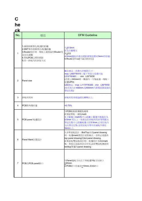
Checklist - PCB Layout11.線路與郵票孔/板邊的距離2.SMT零件與郵票孔/板邊距離3.Router設計時,單板上需預留的Router用定位孔個數4.單板PCB之間的間距5.同一拼板內的拼版方式1.>0.5mm2.見右圖備注3.>2個4.2mm(圓弧形產品間距需要設置成3mm或更寬)5.Route或V-cut(不能同時存在)2Panel size 數位產品:設備允許極限尺寸:max L460*W410(鬆下等部分設備可貼L510*W460),min L50*W50(長度≧240mm時,機器內一次隻能進一塊板,影響UPH)LED產品:max L1170*W250,minL50*W50(如長度大於400mm,每400mm內需要設置兩個光學定位點)3拼板利用率拼板利用率理論需在85%以上. 4PCB對角變形量<0.75%5PCB panel 板邊設計1.PCB板框做導圓弧處理2.預留單板、連板mark3.工藝邊上mark點中心距離工藝邊外側最佳為5.5mm 或以上,如果由於拼板利用率等問題光學定位點中心距離板邊小於5.5mm,必須在板內加光學定位點,並保証板內零件到連板外側在5mm以上.6Panel Mark位置設計1.非單面板設計,Bot/Top共用panel drawing 時,板邊mark需設計成對稱式,否則必須提供top panel drawing和bot panel drawing.2.單面板/雙面板設計時,板邊設計為3個mark 點,對投反面起到防呆作用,此時雙面板應提供bot/top單獨的panel drawing。
7PCB及PCB panel缺口1.Panel進板方向右下角板邊Y軸方向缺口<20mm.2.PCB缺口長寬若>10mm,需補缺口No.項目DFM Guideline8Barcode silk設計1.絲印框填充光滑平整的白油2.對應尺寸見附件9Pin in paste零件設計 1.必須layout在成品生產面2.陰陽板設計時,元件腳不可伸出PCB反面。
1. 目的和作用1.1 规范设计作业,提高生产效率和改善产品的质量。
2. 适用范围1.1 XXX公司开发部的VCD、超级VCD、DVD、音响等产品。
3. 责任3.1 XXX开发部的所有电子工程师、技术员及电脑绘图员等。
4. 资历和培训4.1 有电子技术基础;4.2 有电脑基本操作常识;4.3 熟悉利用电脑PCB绘图软件.5. 工作指导(所有长度单位为MM)5.1 铜箔最小线宽:单面板0.3MM,双面板0.2MM,边缘铜箔最小要1.0MM5.2 铜箔最小间隙:单面板:0.3MM,双面板:0.2MM.5.3 铜箔与板边最小距离为0.5MM,元件与板边最小距离为5.0MM,焊盘与板边最小距离为4.0MM。
5.4 一般通孔安装元件的焊盘的大小(直径)为孔径的两倍,双面板最小为1.5MM,单面板最小为2.0MM,建议(2.5MM)。
如果不能用圆形焊盘,可用腰圆形焊盘,大小如下图所示(如有标准元件库,则以标准元件库为准):焊盘长边、短边与孔的关系为:a B c0.6 2.8 1.270.7 2.8 1.520.8 2.8 1.650.9 2.8 1.741.02.8 1.841.12.8 1.945.5 电解电容不可触及发热元件,如大功率电阻,热敏电阻,变压器,散热器等.电解电容与散热器的间隔最小为10.0MM,其它元件到散热器的间隔最小为2.0MM.5.6 大型元器件(如:变压器、直径15.0MM以上的电解电容、大电流的插座等)加大铜箔及上锡面积如下图;阴影部分面积肥最小要与焊盘面积相等。
5.7 螺丝孔半径5.0MM内不能有铜箔(除要求接地外)及元件.(或按结构图要求).5.8 上锡位不能有丝印油.5.9 焊盘中心距小于2.5MM的,该相邻的焊盘周边要有丝印油包裹,丝印油宽度为0.2MM(建议0.5MM).5.10 跳线不要放在IC下面或马达、电位器以及其它大体积金属外壳的元件下.5.11 在大面积PCB设计中(大约超过500CM2以上),为防止过锡炉时PCB板弯曲,应在PCB板中间留一条5至10MM宽的空隙不放元器件(可走线),以用来在过锡炉时加上防止PCB板弯曲的压条,如下图的阴影区:5.12 每一粒三极管必须在丝印上标出e,c,b脚.5.13 需要过锡炉后才焊的元件,焊盘要开走锡位,方向与过锡方向相反,宽度视孔的大小为0.5MM到1.0MM。
PCB_焊盘工艺设计规范分解焊盘工艺设计规范是指在PCB(Printed Circuit Board,印刷电路板)生产过程中,对焊盘的设计和加工要求的规范。
通过合理的焊盘工艺设计,可以确保焊盘的质量和可靠性,提高PCB的性能和可靠性。
下面将焊盘工艺设计规范进行分解说明:一、焊盘形状设计规范焊盘形状设计是决定焊接方式和焊接质量的关键。
一般焊盘可以分为圆形、方形、椭圆形、矩形等多种形状。
在设计时需要根据元件封装类型、焊接方式、焊接工艺等因素来确定焊盘的形状。
同时,需要考虑焊盘的尺寸大小、间距、焊盘间隙、端子与焊盘的连接等问题。
二、焊盘布局设计规范焊盘布局设计是指焊盘在PCB上的分布和排列。
合理的焊盘布局可以提高元器件的密集度、避免焊接间隙过小和相互干扰等问题。
在布局设计时需要考虑焊盘之间的间距、端子与焊盘之间的间隔、焊盘与其他元器件之间的间距等因素。
三、焊盘间隙设计规范焊盘间隙是指焊盘与焊盘之间的间距。
合理的焊盘间隙可以避免相邻焊盘之间的短路或者过接问题。
焊盘间隙的设计需要根据焊接工艺、焊料类型、焊盘尺寸等因素来确定。
通常,大尺寸焊盘的间隙可以较小,而小尺寸焊盘的间隙则需要适当增大。
四、焊盘涂覆设计规范焊盘涂覆是指在焊盘上涂覆一层焊接助剂,用于提高焊接的质量和可靠性。
合理的焊盘涂覆设计可以提高焊盘的润湿性和耐腐蚀性,同时也能够减少焊接过程中的气泡和其他缺陷。
在涂覆设计时需要考虑涂覆层的厚度、均匀性、涂覆方式等因素。
五、焊盘刚化设计规范焊盘刚化是指通过改变焊盘的材料或者结构来提高焊盘的刚度和稳定性。
焊盘刚化设计需要考虑焊盘的材料选择、厚度、形状等因素。
一般情况下,大功率焊盘需要更高的刚度和稳定性。
六、焊盘检测规范焊盘检测是指对焊盘进行质量检测和可靠性验证。
焊盘检测需要使用相关的测试设备和工具,对焊盘的焊接质量、焊盘与元器件的连接可靠性、焊盘与PCB的连接质量等进行检测。
同时还需要制定相应的测试标准和流程,确保焊盘的质量符合要求。
QFN封装的PCB焊盘和网板设计
一、QFN封装的PCB焊盘设计
1、PCB焊盘的选择:QFN封装的PCB焊盘一般采用多条直线或多个圆
形焊盘,需要选择适当的焊盘形状,其尺寸应根据QFN封装的封装尺寸确定,以确保焊盘的完整性和位置精度。
2、焊盘的形状:QFN封装的PCB焊盘一般采用椭圆形、多条线状或
多个圆形焊盘,其中多条线状焊盘的通路应足够窄,以减少焊锡在焊盘通
路中的迁移。
3、焊盘尺寸:QFN封装的PCB焊盘的尺寸一般比QFN封装的封装尺
寸大,且其宽度也要大于封装宽度,尽可能的增大PCB焊盘的面积,以提
高焊接过程中焊锡的容积,确保焊接强度。
4、焊盘间距:QFN封装的PCB焊盘的间距应做到合理,且不能太近,太近容易影响焊接精度,焊接效果不理想。
二、QFN封装的PCB网板设计
1、网板选择:QFN封装的PCB网板应根据封装的尺寸、焊盘形状和
数量等参数来选定,其选择的网板应当稳定、耐高温,具有良好的焊接强度。
2、网板形状:QFN封装的PCB网板的形状可以采用标准圆形、正方形、长方形等,其尺寸应考虑外形大小、焊盘的形状和数量等参数,确保
网板的焊接质量和稳定性。
3、网板的厚度:QFN封装的PCB网板的厚度要根据使用的焊接温度和焊接深度等参数确定,以适应不同的焊接技术,保证网板的稳定性和焊接强度。
QFN封装的PCB焊盘和网板设计近几年来,由于QFN封装(Quad Flat No-lead package,方形扁平无引脚封装)具有良好的电和热性能、体积小、重量轻,其应用正在快速增长。
采用微型引线框架的QFN封装称为MLF(Micro Lead Frame,微引线框架)封装。
QFN封装和CSP(Chip Size Package,芯片尺寸封装)有些相似,但元件底部没有焊球,与PCB的电气和机械连接是通过PCB焊盘上印刷焊膏经过回流焊形成的焊点来实现的。
QFN封装对工艺提出了新的要求,本文将对PCB焊盘和印刷网板设计进行探讨。
图1:外露散热焊盘的QFN封装QFN封装的特点QFN是一种无引脚封装,呈正方形或矩形,封装底部中央位置有一个大面积裸露焊盘用来导热,围绕大焊盘的封装四周有实现电气连接的导电焊盘。
由于QF N封装不像传统的SOIC与TSOP封装那样具有鸥翼状引线,内部引脚与焊盘之间的导电路径短,自感系数以及封装体内布线电阻很低,所以它能提供卓越的电性能。
此外,它还通过外露的引线框架焊盘提供了出色的散热性能,该焊盘具有直接散热通道,用于释放封装内的热量。
通常将散热焊盘直接焊接在电路板上,PCB中的散热过孔有助于将多余的功耗扩散到铜接地板中,从而吸收多余的热量。
图1显示了这种采用PCB焊接的外露散热焊盘的封装。
由于体积小、重量轻,以及极佳的电性能和热性能,QFN封装特别适合任何一个对尺寸、重量和性能都有要求的应用。
与传统的28引脚PLCC封装相比,32引脚QFN封装的面积(5mm×5mm)缩小了84%,厚度(0.9mm)降低了80%,重量(0.06g)减轻了95%,电子封装寄生效应也降低了50%,所以非常适合应用在手机、数码相机、PDA及其他便携电子设备的高密度PCB上。
PCB焊盘设计QFN的焊盘设计主要包含以下三个方面:周边引脚的焊盘设计、中间热焊盘及过孔的设计和对PCB阻焊层结构的考虑。
在PCB设计中,焊盘是一个非常重要的概念,PCB工程师对它一定不陌生。
不过,虽然熟悉,很多工程师对焊盘的知识却是一知半解。
今天,电路菌带大家来了解下焊盘的种类,以及在PCB设计中焊盘的设计标准。
焊盘,表面贴装装配的基本构成单元,用来构成电路板的焊盘图案(land pattern),即各种为特殊元件类型设计的焊盘组合。
焊盘用于电气连接、器件固定或两者兼备的部分导电图形。
PCB焊盘的种类一、常见焊盘1、方形焊盘——印制板上元器件大而少、且印制导线简单时多采用。
在手工自制PCB时,采用这种焊盘易于实现。
2、圆形焊盘——广泛用于元件规则排列的单、双面印制板中。
若板的密度允许,焊盘可大些,焊接时不至于脱落3、岛形焊盘——焊盘与焊盘间的连线合为一体。
常用于立式不规则排列安装中。
4、多边形焊盘——用于区别外径接近而孔径不同的焊盘,便于加工和装配。
5、椭圆形焊盘——这种焊盘有足够的面积增强抗剥能力,常用于双列直插式器件。
6、开口形焊盘——为了保证在波峰焊后,使手工补焊的焊盘孔不被焊锡封死时常用。
二、特殊焊盘1、梅花焊盘梅花焊盘通常用在大的过孔接地的位置,这样设计有以下几点原因:1)固定孔需要金属化和GND相连,如果该固定孔是全金属化的,在回流焊的时候容易将该孔堵住。
2)采用内部的金属螺孔可能由于安装或多次拆装等原因,造成该接地处于不良的状态。
而采用梅花孔焊盘,不管应力如何变化,均能保证良好的接地。
2、十字花焊盘十字花焊盘又称热焊盘、热风焊盘等。
其作用是减少焊盘在焊接中向外散热,以防止因过度散热而导致的虚焊或PCB起皮。
1)当你的焊盘是地线时候。
十字花可以减少连接地线面积,减慢散热速度,方便焊接。
2)当你的PCB是需要机器贴片,并且是回流焊机,十字花焊盘可以防止PCB起皮(因为需要更多热量来融化锡膏)。
3、泪滴焊盘当焊盘连接的走线较细时常采用,以防焊盘起皮、走线与焊盘断开。
这种焊盘常用在高频电路中。
PCB设计中焊盘的设计标准一、PCB焊盘的形状和尺寸设计标准:1、调用PCB标准封装库。