数字集成电路(电路系统与设计)第3章习题
- 格式:pdf
- 大小:17.72 MB
- 文档页数:10
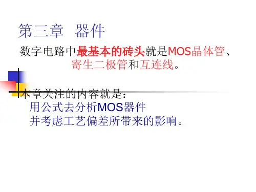
习题参考解答第1章基本知识1.什么是数字信号?什么是模拟信号?(注:所有蓝色标题最后均去掉!)答案:数字信号:指信号的变化在时间上和数值上都是断续的,或者说是离散的,这类信号有时又称为离散信号。
例如,在数字系统中的脉冲信号、开关状态等。
模拟信号:指在时间上和数值上均作连续变化的信号。
例如,温度、交流电压等信号。
2.数字系统中为什么要采用二进制?答案:二进制具有运算简单、物理实现容易、存储和传送方便、可靠等优点。
3.机器数中引入反码和补码的主要目的是什么?答案:将减法运算转化为加法运算,统一加、减运算,使运算更方便。
4.BCD码与二进制数的区别是什么?答案:二进制数是一种具有独立进位制的数,而BCD码是用二进制编码表示的十进制数。
5.采用余3码进行加法运算时,应如何对运算结果进行修正?为什么?答案:两个余3码表示的十进制数相加时,对运算结果修正的方法是:如果有进位,则结果加3;如果无进位,则结果减3。
为了解决四位二进制运算高位产生的进位与一位十进制运算产生的进位之间的差值。
6.奇偶检验码有哪些优点和不足?答案:奇偶检验码的优点是编码简单,相应的编码电路和检测电路也简单。
缺点是只有检错能力,没有纠错能力,其次只能发现单错,不能发现双错。
7.按二进制运算法则计算下列各式。
答案:(1)110001 (2)110.11 (3)10000111 (4)1018.将下列二进制数转换成十进制数、八进制数和十六进制数。
答案:(1)(117)10 ,(165)8 ,(75)16(2)(0.8281)10 ,(0.65)8 ,(0.D4)16(3)(23.25)10 ,(27.2)8 ,(17. 4)169.将下列十进制数转换成二进制数、八进制数和十六进制数(精确到二进制小数点后4位)。
答案:(1)(1000001)2 ,(101)8 ,(41)16(2)(0.0100)2 ,(0.20)8 ,(0.40)16(3)(100001.0101)2 ,(41.24)8 ,(21.50)1610.写出下列各数的原码、反码和补码。
《数字电路与逻辑设计》作业教材:《数字电子技术基础》(高等教育出版社,第2版,2012年第7次印刷)第一章:自测题:一、1、小规模集成电路,中规模集成电路,大规模集成电路,超大规模集成电路5、各位权系数之和,1799、,,;,,二、1、×8、√10、×三、1、A4、B练习题:1.3、解:(1) 十六进制转二进制: 4 5 C0100 0101 1100二进制转八进制:010 001 011 1002 13 4十六进制转十进制:(45C)16=4*162+5*161+12*160=(1116)10所以:(45C)16=(10001011100)2=(2134)8=(1116)10(2) 十六进制转二进制: 6 D E . C 80110 1101 1110 . 1100 1000 二进制转八进制:011 011 011 110 . 110 010 0003 3 3 6 . 6 2十六进制转十进制:(6DE.C8)16=6*162+13*161+14*160+13*16-1+8*16-2=(1758.78125)10 所以:(6DE.C8)16=(0. 11001000)2=(3336.62)8=(1758.78125)10(3) 十六进制转二进制:8 F E . F D1000 1111 1110. 1111 1101二进制转八进制:100 011 111 110 . 111 111 0104 3 7 6 . 7 7 2十六进制转十进制:(8FE.FD)16=8*162+15*161+14*160+15*16-1+13*16-2=(2302.98828125)10 所以:(8FE.FD)16=(1.11111101)2=(437 6.772)8=(2302.98828125)10(4) 十六进制转二进制:7 9 E . F D0111 1001 1110 . 1111 1101二进制转八进制:011 110 011 110 . 111 111 0103 6 3 6 . 7 7 2十六进制转十进制:(79E.FD)16=7*162+9*161+14*160+15*16-1+13*16-2=(1950. )10 所以:(8FE.FD)16=0.11111101)2=(3636.772)8=(1950.98828125)101.5、解:(74)10 =(0111 0100)8421BCD=(1010 0111)余3BCD(45.36)10 =(0100 0101.0011 0110)8421BCD=(0111 1000.0110 1001 )余3BCD(136.45)10 =(0001 0011 0110.0100 0101)8421BCD=(0100 0110 1001.0111 1000 )余3BCD (374.51)10 =(0011 0111 0100.0101 0001)8421BCD=(0110 1010 0111.1000 0100)余3BCD1.8、解(1)(+35)=(0 100011)原= (0 100011)补(2)(+56 )=(0 111000)原= (0 111000)补(3)(-26)=(1 11010)原= (1 11101)补(4)(-67)=(1 1000011)原= (1 1000110)补。
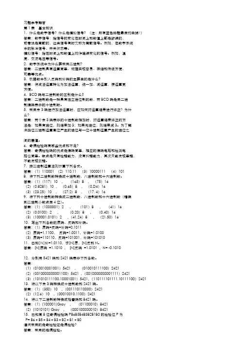
第三章场效应晶体管及其电路分析题1.3.1绝缘栅场效应管漏极特性曲线如图题1.3.1(a)~(d)所示。
(1)说明图(a)~(d)曲线对应何种类型的场效应管。
(2)根据图中曲线粗略地估计:开启电压V T、夹断电压V P和饱和漏极电流I DSS或I DO 的数值。
图题1.3.1解:图(a):增强型N沟道MOS管,V GS(th)≈3V,I DO≈3mA;图(b):增强型P沟道MOS管,V GS(th)≈-2V,I DO≈2mA;图(c):耗尽型型P沟道MOS管,V GS(off)≈2V,I DSS≈2mA;图(d):耗尽型型N沟道MOS管,V GS(off)≈-3V,I DSS≈3mA。
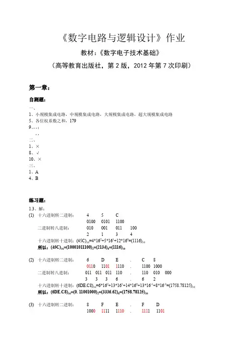
题1.3.2 场效应管漏极特性曲线同图题1.3.1(a)~(d)所示。
分别画出各种管子对应的转移特性曲线i D=f(v GS)。
解:在漏极特性上某一V DS下作一直线,该直线与每条输出特性的交点决定了V GS和I D的大小,逐点作出,连接成曲线,就是管子的转移特性了,分别如图1.3.2所示。
图1.3.2题1.3.3 图题1.3.3所示为场效应管的转移特性曲线。
试问:图题1.3.3(1)I DSS 、V P 值为多大? (2)根据给定曲线,估算当i D =1.5mA 和i D =3.9mA 时,g m 约为多少? (3) 根据g m 的定义:GS Dm dv di g ,计算v GS = -1V 和v GS = -3V 时相对应的g m 值。
解: (1) I DSS =5.5mA ,V GS(off)=-5V ;(2) I D =1.5mA 时,g m ≈0.88ms ,I D =3.9mA 时,g m ≈1.76ms ;(3) v GS =-1V 时,g m ≈0.88ms ,v GS =-3V 时,g m ≈1.76ms 。
题1.3.4 由晶体管特性图示仪测得场效应管T 1和T 2各具有图题1.3.4的(a )和(b )所示的输出 特性曲线,试判断它们的类型,并粗略地估计V P 或V T 值,以及v DS =5V 时的I DSS 或 I DO 值。
思考题:题3.1.1 组合逻辑电路在结构上不存在输出到输入的 ,因此 状态不影响 状态。
答:反馈回路、输出、输入。
题3.1.2 组合逻辑电路分析是根据给定的逻辑电路图,而确定 。
组合逻辑电路设计是根据给定组合电路的文字描述,设计最简单或者最合理的 。
答:逻辑功能、逻辑电路。
题3.2.1 一组合电路输入信号的变化顺序有以下三种情况,当 时,将可能出现竞争冒险。
(A )00→01→11→10 (B )00→01→10→11 (C )00→10→11→01 答:B题3.2.2 清除竞争冒险的常用方法有(1)电路输出端加 ;(2)输入加 ;(3)增加 。
答:电容,选通脉冲,冗余项。
题3.2.3 门电路的延时时间是产生组合逻辑电路竞争与冒险的唯一原因。
( ) 答:×题3.2.4 根据毛刺产生的方向,组合逻辑的冒险可分为 冒险和 冒险。
答:1型、0型。
题3.2.5 传统的判别方法可采用 和 法来判断组合电路是否存在冒险。
答:代数法、卡诺图。
题3.3.1 进程行为之间执行顺序为 ,进程行为内部执行顺序为 。
答:同时、依次。
题3.3.2 行为描述的基本单元是 ,结构描述的基本单元是 。
答:进程、调用元件语句。
题3.3.3 结构体中的每条VHDL 语句的执行顺序与排列顺序 。
答:无关题3.4.1串行加法器进位信号采用 传递,而并行加法器的进位信号采用 传递。
(A )超前,逐位 (B )逐位,超前 (C )逐位,逐位 (D )超前,超前 答:B题3.4.2 一个有使能端的译码器作数据分配器时,将数据输入端信号连接在 。
答:使能端题 3.4.3 优先编码器输入为70I I -(0I 优先级别最高),输出为2F 、1F 、0F (2F 为高位)。
当使能输入00,651====I I I S 时,输出012F F F 应为 。
答:110题3.4.4 用4位二进制比较器7485实现20位二进制数并行比较,需要 片。
CHAPTER 3P3.1. The general approach for the first two parameters is to figure out which variables shouldremain constant, so that when you have two currents, you can divide them, and every variable but the ones you want to calculate remain. In this case, since the long-channel transistor is in saturation for all values of V GS and V DS , only one equation needs to be considered:()()2112DS N OX GS T DS W I C V V V Lμλ=-+ For the last two parameters, now that you have enough values, you can just choose oneset of numbers to compute their final values.a. The threshold voltage, V T0, can be found by choosing two sets of numbers with the same V DS ’s but with different V GS ’s. In this case, the first two values in the table can be used.()()()()()()211122222201022001121121.2 1.210000.82800.8DS N OX GS T DS DS N OX GS T DS T DS T DS T T W I C V V V L W I C V V V LV I V I V V μλμλ=-+=-+-⎛⎫-===⎪--⎝⎭ 00.35V T V ∴=b. The channel modulation parameter, λ, can be found by choosing two sets of numberswith the same V GS ’s but with different V DS ’s. In this case, the second and third values in the table can be used.()()221 1.225010.8247DS DS I I λλ+==+ -10.04V λ∴=c. The electron mobility, µn , can now be calculated by looking at any of the first three sets of numbers, but first, let’s calculate C OX .631062-31m 10μm22?.210μm1m 10 0.0351 1.610/2.210OX OX t C F cm--=⨯⨯===⨯Now calculate the mobility by using the first set of numbers.()()()()()()()()()()()()22111021262101111 1.21 1.222210002cm 348V-s 1.610(4.75)1.20.3510.04 1.21DS N OX GS T DS N OX T DS N OX GS T DS W W I C V V V C V L LA I W C V V V L μλμλμμλ-=-+=-+===⨯-+-+d. The body effect coefficient gamma, γ, can be calculated by using the last set of numbers since it is the only one that has a V SB greater than 0V.()()()()244124414411221 1.20.468VDS N OX GS T DS DS GS T N OX DS GS T T GS W I C V V V LI V V W C V LV V V V μλμλ=-+-=+-==-==12000.6VT T T T V V V V γγγ=+-====P3.2. The key to this question is to identify the transistor’s region of operation so that gatecapacitance may be assigned appropriately, and the primary capacitor that will dischargedat a rate of V It C ∂∂= by the current source may be identified. Then, because the nodes arechanging, the next region of operation must be identified. This process continues until the transistor reaches steady state behavior. Region 1:Since 0V GS V = the transistor is in the cutoff region. The gate capacitance is allocated to GB C . Since no current will flow through the transistor, all current will come from the source capacitor and the drain node remains unchanged.68-151010V V 6.67100.6671510s nsSB V I I t C C -∆⨯====⨯=∆⨯ The source capacitor will discharge until 1.1V GS T V V == when the transistor enters thesaturation region. This would require that the source node would be at 3.3 1.1 2.2V S G GS V V V =-=-=.()15961510 3.3 2.2 1.6510s 1.65ns 1010C t V I ---⨯∆=∆=-=⨯=⨯ Region 2:The transistor turns on and is in saturation. The current is provided from the capacitor atthe drain node, while the source node remains fairly constant. The capacitance at the drain node is the same as the source node so the rate of change is given by:68-151010V V 6.67100.6671510s nsSB V I I t C C -∆⨯====⨯=∆⨯ Since the transistor is now in the saturation region, GS V can be computed based on thecurrent flowing through the device.()22 1.1 1.37V 3.3 1.37 1.93VGS T GST S G GS kW I V V LV V V V V =-==+==-=-=This is where the source node settles. This means that most of the current is discharged through the transistor until the drain voltage reaches a value that puts the transistor at the edge of saturation.3.3 1.1 2.2VDS GS TD G T V V V V V V =-=-=-=If we assume that all the current comes from the transistor, and the source node remains fixed, the drain node will then discharge at a rate equal to that of the source node in the first region. Region 3:The transistor is now in the linear region the gate capacitance is distributed equally to both GS C and GD C . and both capacitors will discharge at approximately the same rate.-151510V0.28621510510nsV I A t C μ-∆===∆⨯⨯+⨯The graph is shown below.00.511.522.533.5024681012Time (ns)V o l t a g e (V )P3.3. The gate and drain are connected together so that DS GS V V = which will cause thetransistor to remain in saturation. This is a dc measurement so capacitances are not required. Connect the bulk to ground and run SPICE. P3.4. Run SPICE. P3.5. Run SPICE. P3.6. Run SPICE. P3.7. Run SPICE.P3.8. First, let’s look at the various parameters and identify how they affect V T .∙ L – Shorter lengths result in a lower threshold voltage due to DIBL. ∙ W – Narrow width can increase the threshold voltage.∙ V SB – Larger source-bulk voltages (in magnitude) result in a higher threshold voltage. ∙ V DS –Larger drain-source voltages (in magnitude) result in a lower threshold voltage due to DIBL. The transistor with the lowest threshold voltage has the shortest channel, larger width, smallest source-bulk voltage and largest drain-source voltage. This would be the first transistor listed.The transistor with the highest threshold voltage has the longest channel, smallest width,largest source-bulk voltage and smallest drain-source voltage. This would be the last transistor listed. P3.9. Run SPICE.P3.10. Run SPICE. The mobility degradation at high temperatures reduces I on and the increasemobile carriers at high temperatures increase I off . P3.11. The issues that prompted the switch from Al to Cu are resistance and electromigration.Copper wires have lower resistances and are less susceptible to electromigration problems. Copper on the other hand, reacts with the oxygen in SiO 2 and requires cladding around the wires to prevent this reaction.For low-k dielectrics, the target value future technologies is 2.High-k dielectrics are being developed as the gate-insulator material of MOSFET’s. This is because the current insulator material, SiO 2, can not be scaled any longer due to tunneling effects.P3.12. Self-aligned poly gates are fabricated by depositing oxide and poly before the source anddrain regions are implanted. Self-aligned silicides (salicides) are deposited on top of the source and drain regions using the spacers on the sides of the poly gate. P3.13. To compute the length, simply use the wire resistance equation and solve for L .LR TWRTWL ρρ==First convert the units of ρ to terms of μm. Aluminum:2.7μΩρ=cm 6Ω10μΩ⨯610μm100cm ⨯()()()0.027Ωμm1000.812963μm 2.96mm0.027RTWL ρ=====Copper:1.7μΩρ=cm 6Ω10μΩ⨯610μm100cm ⨯()()()0.017Ωμm1000.814706μm 4.71mm0.017RTWL ρ=====P3.14. Generally, the capacitance equation in terms of permittivity constants and spacing is:k C WL tε=a. 4k = ()()()()230048.8510 3.541100SiO k k C WL TL t S S Sεε-====b. 2k = ()()()()30028.8510 1.771100k k C WL TL t S SSεε-====The plots are shown below.Capacitance vs. Spacing01234567800.511.522.533.544.555.5Spacing (um)C a p a c i t a n c e (f F)。
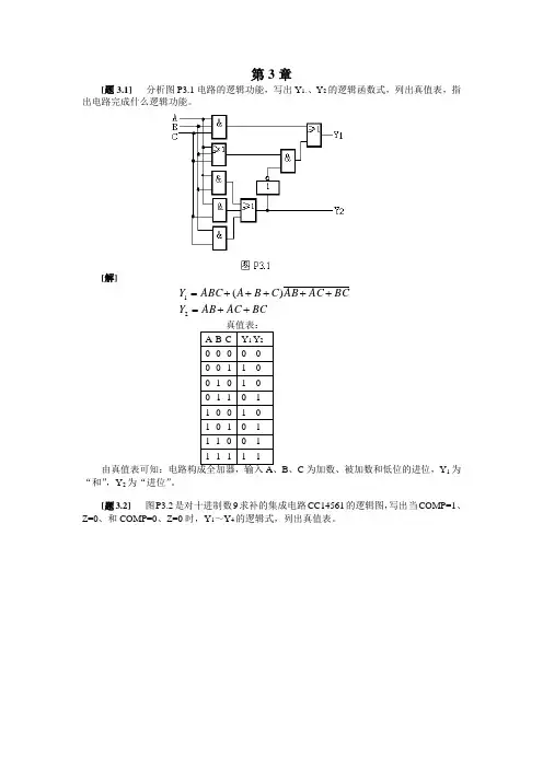
第3章[题3.1] 分析图P3.1电路的逻辑功能,写出Y 1、、Y 2的逻辑函数式,列出真值表,指出电路完成什么逻辑功能。
[解]BCAC AB Y BCAC AB C B A ABC Y ++=+++++=21)(B 、C 为加数、被加数和低位的进位,Y 1为“和”,Y 2为“进位”。
[题3.2] 图P3.2是对十进制数9求补的集成电路CC14561的逻辑图,写出当COMP=1、Z=0、和COMP=0、Z=0时,Y 1~Y 4的逻辑式,列出真值表。
[解](1)COMP=1、Z=0时,TG 1、TG 3、TG 5导通,TG 2、TG 4、TG 6关断。
3232211 , ,A A Y A Y A Y ⊕===, 4324A A A Y ++=(2)COMP=0、Z=0时,Y 1=A 1, Y 2=A 2, Y 3=A 3, Y 4=A 4。
COMP =0、Z=0的真值表从略。
[题3.3] 用与非门设计四变量的多数表决电路。
当输入变量A 、B 、C 、D 有3个或3个以上为1时输出为1,输入为其他状态时输出为0。
[解] 题3.3的真值表如表A3.3所示,逻辑图如图A3.3所示。
ABCD D ABC D C AB CD B A BCD A Y ++++= BCD ACD ABC ABC +++=B C D A C D A B D A B C ⋅⋅⋅=[题3.4] 有一水箱由大、小两台泵M L 和M S 供水,如图P3.4所示。
水箱中设置了3个水位检测元件A 、B 、C 。
水面低于检测元件时,检测元件给出高电平;水面高于检测元件时,检测元件给出低电平。
现要求当水位超过C 点时水泵停止工作;水位低于C 点而高于B 点时M S 单独工作;水位低于B 点而高于A 点时M L 单独工作;水位低于A 点时M L 和M S 同时工作。
试用门电路设计一个控制两台水泵的逻辑电路,要求电路尽量简单。
[解] 题3.4的真值表如表A3.4所示。
数字电路习题库1.单元习题库及答案第一章(选择、判断共20题)一、选择题1.以下代码中为无权码的为。
a.8421bcd码b.5421bcd码c.余三码d.格雷码2.以下代码中为恒权码的为。
a.8421bcd码b.5421bcd码c.余三码d.格雷码3.一位十六进制数可以用位二进制数去则表示。
a.1b.2c.4d.164.十进制数25用8421bcd码则表示为。
a.10101b.00100101c.100101d.101015.在一个8位的存储单元中,能够存储的最大无符号整数是。
a.(256)10b.(127)10c.(ff)16d.(255)106.与十进制数(53.5)10等值的数或代码为。
a.(01010011.0101)8421bcdb.(35.8)16c.(110101.1)2d.(65.4)87.矩形脉冲信号的参数存有。
a.周期b.占空比c.脉宽d.扫描期8.与八进制数(47.3)8等值的数为:a.(100111.011)7.3)2b.(27.6)16c.(216d.(100111.11)29.常用的bcd码有。
a.奇偶校验码b.格雷码c.8421码d.余三码10.与模拟电路相比,数字电路主要的优点有。
a.难设计b.通用性弱c.保密性不好d.抗干扰能力弱二、判断题(正确打√,错误的打×)1.方波的占空比为0.5。
()2.8421码1001比0001大。
()3.数字电路中用“1”和“0”分别则表示两种状态,二者并无大小之分后。
()4.格雷码具备任何相连码只有一位码元相同的特性。
()5.八进制数(18)8比十进制数(18)10大。
()6.当传送十进制数5时,在8421奇校验码的校验位上值应为1。
(7.在时间和幅度上都断续变化的信号是数字信号,语音信号不是数字信号。
()8.充电电流的公式为:q=tw/t,则周期t越大充电电流q越大。
()9.十进制数(9)10比十六进制数(9)16大。
第一章绪论一、填空题1、根据集成度的不同,数字集成电路分位以下四类:小规模集成电路、中规模集成电路、大规模集成电路、超大规模集成电路。
2、二进制数是以2为基数的计数体制,十六体制数是以16为基数的计数体制。
3、二进制数只有0和1两个数码,其计数的基数是2,加法运算的进位规则为逢二进一。
4、十进制数转换为二进制数的方法是:整数部分用除2取余法,小数部分用乘2取整法,十进制数23.75对应的二进制数为10111.11。
5、二进制数转换为十进制数的方法是各位加权系数之和,二进制数10110011对应的十进制数为179。
6、用8421BCD码表示十进制时,则每位十进制数可用四位二进制代码表示,其位权值从高位到低位依次为8、4、2、1。
7、十进制数25的二进制数是11001,其对应的8421BCD码是00100101。
8、负数补码和反码的关系式是:补码=反码+1。
9、二进制数+1100101的原码为01100101,反码为01100101,补码为01100101。
-1100101的原码为11100101,反码为10011010,补码为10011011。
10、负数-35的二进制数是-100011,反码是1011100,补码是1011101。
二、判断题1、二进制数有0~9是个数码,进位关系为逢十进一。
()2、格雷码为无权码,8421BCD码为有权码。
(√)3、一个n位的二进制数,最高位的权值是2^n+1。
(√)4、十进制数证书转换为二进制数的方法是采用“除2取余法”。
(√)5、二进制数转换为十进制数的方法是各位加权系之和。
(√)6、对于二进制数负数,补码和反码相同。
()7、有时也将模拟电路称为逻辑电路。
()8、对于二进制数正数,原码、反码和补码都相同。
(√)9、十进制数45的8421BCD码是101101。
()10、余3BCD码是用3位二进制数表示一位十进制数。
()三、选择题1、在二进制技术系统中,每个变量的取值为(A)A、0和1B、0~7C、0~10D、0~F2、二进制权值为(B )A、10的幂B、2的幂C、8的幂D、16的幂3、连续变化的量称为(B )A、数字量B、模拟量C、二进制量D、16进制量4、十进制数386的8421BCD码为(B)A、0011 0111 0110B、0011 1000 0110C、1000 1000 0110D、0100 1000 01105、在下列数中,不是余3BCD码的是(C )A、1011B、0111C、0010D、10016、十进制数的权值为(D )A、2的幂B、8的幂C、16的幂D、10的幂7、负二进制数的补码等于(D )A、原码B、反码C、原码加1D、反码加18、算术运算的基础是 ( A )A 、加法运算B 、减法运算C 、乘法运算D 、除法运算9、二进制数-1011的补码是 ( D )A 、00100B 、00101C 、10100D 、1010110、二进制数最高有效位(MSB )的含义是 ( A )A 、最大权值B 、最小权值C 、主要有效位D 、中间权值第二章 逻辑代数基础一、填空题1、逻辑代数中三种最基本的逻辑运算是与运算、或运算、非运算。
思考题与习题与题解3-1 填空题1.若要实现逻辑函数BC AB F +=,可以用一个 1 与或 门;或者用 三 个与非门;或者用 四 个或非门。
2.半加器有 2 个输入端, 2 个输出端;全加器有 3 个输入端, 2 个输出端。
3. 半导体数码显示器的内部接法有两种形式:共 阴极 接法和共 阳极 接法。
4. 对于共阳接法的发光二极管数码显示器,应采用 低 电平驱动的七段显示译码器。
3-2 单项选择题1.组合逻辑电路的输出取决于( A )。
A .输入信号的现态B .输出信号的现态C .输入信号的现态和输出信号变化前的状态 2.编码器译码器电路中,( A )电路的输出是二进制代码。
A .编码 B .译码 C .编码和译码 3.全加器是指( C )。
A .两个同位的二进制数相加B .不带进位的两个同位的二进制数相加C .两个不同位的二进制数及来自低位的进位三者相加 4.二-十进制的编码器是指( B )。
A .将二进制代码转换成0~9十个数字B .将0~9十个数字转换成二进制代码电路C .二进制和十进制电路 5.二进制译码器指( A )。
A .将二进制代码转换成某个特定的控制信息B .将某个特定的控制信息转换成二进制数C .具有以上两种功能6. 组合电路的竞争冒险是指( B )。
A .输入信号有干扰时,在输出端产生了干扰脉冲B .输入信号改变状态时,输出端可能出现的虚假信号C .输入信号不变时,输出端可能出现的虚假信号3-3 组合电路如图图3.45所示,分析该电路的逻辑功能。
图3.45 题3-3图图(a) C B A ABC C B A ABC ABC CABC B ABC A L +=++=++=)( 图(b)[][][][][][]))(())(()()()()(D C D C B A AB D C CD B A B A D C D C B A B A D C B A Y +++++=+⊕+=⊕⊕⊕=(2)由表达式列出真值表,见表3-1 (a)、(b)。
第1 章计算机系统概述【1-1】简答题(1)计算机字长(Word)指的是什么?(2)处理器的“取指-译码-执行周期”是指什么?(3)总线信号分成哪3 组信号?(4)外部设备为什么又称为I/O 设备?(5)Windows 的控制台窗口与模拟DOS 窗口有什么不同?[答案](1)处理器每个单位时间可以处理的二进制数据位数称计算机字长。
(2)指令的处理过程。
处理器的“取指—译码—执行周期” 是指处理器从主存储器读取指令(简称取指),翻译指令代码的功能(简称译码),然后执行指令所规定的操作(简称执行)的过程。
(3)总线信号分成3 组,分别是数据总线、地址总线和控制总线。
(4)因为外设以输入(Input)和输出(Output)形式与主机交换数据。
(5)Windows 的控制台窗口是基于32/64 位Windows 操作系统,模拟DOS 窗口是基于16 位DOS 操作系统。
【1-2】判断题(1)处理器是计算机的控制中心,内部只包括5 大功能部件的控制器。
(2)处理器并不直接连接外设,而是通过I/O 接口电路与外设连接。
(3)处理器进行读操作,就是把数据从处理器内部读出传送给主存或外设。
【读操作是数据由模块到主模块的数据传送,写操作是数据由主模块到从模块的数据传送。
】(4)软件与硬件的等价性原理说明软硬件在功能、性能和成本等方面是等价的。
【软件和硬件的等价性原理是什么?特点?答:理论上,任何一个由软件所完成的操作也可以直接由硬件来实现,任何一条由硬件所执行的指令也能用软件来完成。
特点:软件易于实现各种逻辑和运算功能,但是往往速度较慢;硬件则可以高速实现逻辑和运算功能,但是难以实现复杂功能或计算。
】(5)支持USB 2.0 版本的USB 设备一定能够以高速(480Mb/s)传输数据。
【USB2.0最高理论带宽是480Mb/s,USB3.0最高理论带宽是5Gb/s.】[答案](1)错(2)对(3)错(4)错(5)错【1-3】填空题(1)CPU 是英文___________的缩写,中文译为___________,微型机采用___________ 芯片构成CPU。
数字集成电路——电路、系统与设计目录第一部分基本单元第1章引论1.1 历史回顾1.2 数字集成电路设计中的问题1.3 数字设计的质量评价1.4 小结1.5 进一步探讨第2章制造工艺2.1 引言2.2 CMOS集成电路的制造2.3 设计规则——设计者和工艺工程师之间的桥梁2.4 集成电路封装2.5 综述:工艺技术的发展趋势2.6 小结2.7 进一步探讨设计方法插入说明A——IC版图第3章器件3.1 引言3.2 二极管3.3 MOS(FET)晶体管3.4 关于工艺偏差3.5 综述:工艺尺寸缩小3.6 小结3.7 进一步探讨设计方法插入说明B——电路模拟第4章导线4.1 引言4.2 简介4.3 互连参数——电容、电阻和电感4.4 导线模型4.5 导线的SPICE模型4.6 小结4.7 进一步探讨第二部分电路设计第5章CMOS反相器5.1 引言5.2 静态CMOS反相器——直观综述5.3 CMOS反相器稳定性的评估——静态特性5.4 CMOS反相器的性能——动态特性5.5 功耗、能量和能量延时5.6 综述:工艺尺寸缩小及其对反相器衡量指标的影响5.7 小结本文由整理提供5.8 进一步探讨第6章CMOS组合逻辑门的设计6.1 引言6.2 静态CMOS设计6.3 动态CMOS设计6.4 设计综述6.5 小结6.6 进一步探讨设计方法插入说明C——如何模拟复杂的逻辑电路设计方法插入说明D——复合门的版图技术第7章时序逻辑电路设计7.1 引言7.2 静态锁存器和寄存器7.3 动态锁存器和寄存器7.4 其他寄存器类型7.5 流水线:优化时序电路的一种方法7.6 非双稳时序电路7.7 综述:时钟策略的选择7.8 小结7.9 进一步探讨第三部分系统设计第8章数字IC的实现策略8.1 引言8.2 从定制到半定制以及结构化阵列的设计方法8.3 定制电路设计8.4 以单元为基础的设计方法8.5 以阵列为基础的实现方法8.6 综述:未来的实现平台8.7 小结8.8 进一步探讨设计方法插入说明E——逻辑单元和时序单元的特性描述设计方法插入说明F——设计综合第9章互连问题9.1 引言9.2 电容寄生效应9.3 电阻寄生效应9.4 电感寄生效应9.5 高级互连技术9.6 综述:片上网络9.7 小结9.8 进一步探讨第10章数字电路中的时序问题10.1 引言10.2 数字系统的时序分类本文由整理提供10.3 同步设计——一个深入的考察10.4 自定时电路设计10.5 同步器和判断器10.6 采用锁相环进行时钟综合和同步10.7 综述:未来方向和展望10.8 小结10.9 进一步探讨设计方法插入说明G——设计验证第11章设计运算功能块11.1 引言11.2 数字处理器结构中的数据通路11.3 加法器11.4 乘法器11.5 移位器11.6 其他运算器11.7 数据通路结构中对功耗和速度的综合考虑11.8 综述:设计中的综合考虑11.9 小结11.10进一步探讨第12章存储器和阵列结构设计12.1 引言12.2 存储器内核12.3 存储器外围电路12.4 存储器的可靠性及成品率12.5 存储器中的功耗12.6 存储器设计的实例研究12.7 综述:半导体存储器的发展趋势与进展12.8 小结12.9 进一步探讨设计方法插入说明H——制造电路的验证和测试本文由整理提供。
第1章习题1.1 名词解释PROM CPLD FPGA ASICJTAG边界扫描FPGA/CPLD编程与配置逻辑综合PAL EDA GAL IP-CORE ISP ASIC RTL FPGA SOPC CPLDIP-CORE SOC和SOPC EDA/CAD1.2 现代EDA技术的特点有哪些?采用HDL描述、自顶向下、开放标准、具有完备设计库1.3 什么是Top-down设计方式?(P4)1.4 数字系统的实现方式有哪些?各有什么优缺点?74LS系列/4000系列常规逻辑门设计:设计难度大、调试复杂采用CPLD/FPGA等可编程器件来设计:用HDL描述、设计难度小、调试仿真方便,开发费用低,但单位成本较高,适合小批量应用专用集成电路设计:设计掩模成本高,适合大批量应用1.5什么是IP复用技术?IP核对EDA技术的应用和发展有什么意义?(P5)IP可重复使用的一种功能设计,可节省设计时间、缩短开发周期,避免重复劳动为大规模SOC设计提供开发基础、和开发平台。
1.6 用硬件描述语言设计数字电路有什么优势?优势:可进行行为级、RTL级、门级多层面对电路进行描述、可功能仿真时序分析,与工艺无关。
1.8 基于FPGA/CPLD的数字系统设计流程包括哪些步骤?(P8 图1.7)1.9 什么是综合?常用的综合工具有哪些?HDL→RTL→门级→网表的描述转换过程ALTERA:MAX-PLUSII,Quartus, Xilinx:ISE , Lattice: ispLERVER1.10 功能仿真与时序仿真有什么区别?功能仿真不考虑器件延时,而时序分析必须考虑在不同器件中的物理信号的延时1.11 数字逻辑设计描述分哪几个层级,各有什么特点。
1.12、为何任意组合逻辑电路可用通用的与阵列、或阵列组合来实现。
可表示为布尔代数方程,由乘积项的和表示1.13 FPGA与CPLD在实现方式或内部结构上的主要区别查表、与或阵列1.14 VerilogHDL与计算机程序设计语言主要区别(描述并行电路行为或结构、描述的串行指令流)1.15 简述“逻辑综合”功能作用。