电子元器件资料
- 格式:pdf
- 大小:273.79 KB
- 文档页数:14
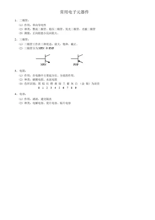
常用电子元器件1、二极管:(1)作用:单向导电性(2)种类:整流二极管、稳压二极管、发光二极管、光敏二极管(3)测量:正向阻值小反向阻大。
2、三极管:(1)三极管工作在三种状态:放大,饱和,截止。
(2)三极管分为NPN 和PNPNPN PNP3、电阻:(1)作用:在电路中主要起分压、分流的作用。
(2)种类:碳膜电阻、水泥电阻(3)色环识别:黑棕红橙黄绿兰紫灰白(金银)为误差0 1 2 3 4 5 6 7 8 94、电容:(1)作用:滤波,通交隔直(2)种类:电解电容、瓷片电容、贴片电容一、AB-6A-402系统(一)AB-6A-402系统配置1、主机型号:AB-6A-402D-B1 AB-6A-402CD-B1AB-6A-402D-A1 AB-6A-402CD-A1AB-6A-402D-E2 AB-6A-402CD-E22、室内分机:AB-6A-402M-C AB-6A-402CM-CAB-6A-402M-B AB-6A-402CM-BAB-6A-402MQ-F AB-6A-402CMQ-FAB-6A-402MQ-F1 AB-6A-402CMQ-F1AB-6A-402CMQ-GAB-6A-402CMQ-G2AB-6A-402CMQ-EAB-6A-402CMQ-I3、隔离器:AB-6A-402A-2 AB-6A-402B-2AB-6A-402A-4 AB-6A-402B-4AB-6A-402A-6 AB-6A-402B-6AB-6A-402A-8 AB-6A-402B-84、电源:门口主机电源:UPS—DP围墙机电源:UPS—DP分机电源:UPS—P管理机电源:UPS—CP其它设备电源:UPS—P5、管理机:AB-6A-602C6、围墙机:AB-6A-602WD7、信号中继器:AB-6A-602SR8、多门选择器:AB-6A-602DS9、联网切换器:AB-6A-602V AP10、视频放大器:AB-6A-602VB(二)系统原理图1、AB-6A-402楼内系统图RVVP3x0.75+SYV-75-5RVV3x0.5+SYV-75-3UPS-P联网主干线上层隔离器RVV2x0.75UPS-DP1FRVV3x0.5402D 电控锁主机1011022022FRVV7x0.3+SYV-75-3隔离器 402RVV2x0.75 1.红线 +12V 2.黑线 GND 3.黄线 LOCK1.红 +15V2.黑 GND3.黄 VIDEO1.红 +12V2.黑 GND3.黄 HOOK4.绿 AUDIO5.棕 DOOR6.橙 CALL1.黑/白 GND2.黄 V-GND3.绿 AUDIO4.棕 DATA5.橙 VIDEO隔离器 402门磁信号检测RVV2x0.52、AB-6A-401楼内系统图隔离器 401RVVP3x0.75RVV3x0.5UPS-P联网主干线上层隔离器RVV2x0.75UPS-DP1FRVV3x0.5401D电控锁主机1011022022FRVV6x0.3隔离器 401RVV2x0.75 1.红线 +12V 2.黑线 GND 3.黄线 LOCK1.红 +12V2.黑 GND3.黄 HOOK4.绿 AUDIO5.棕 DOOR6.橙 CALL1.绿 AUDIO2.棕 DATA3.橙 GND门磁信号检测RVV2x0.5(三)常见故障分析 1、门口主机上电不自检是否空中对插线是否接好(或电源正负是否接好)门口主机上电不自检接好是更换测量供主机电源电压是否正常保险管是否烧掉自恢保险丝是否有发烫否是是二极管是否击穿是更换否220交流有无接入主机电源接好否接好否是变压器是否接好变压器是否坏掉是是更换变压器否电源主板坏说明:门口主机上电不自检一般:(1) ZD1 13V 二极管击穿。

电子元器件基础知识培训教材一、引言在现代电子技术领域,电子元器件是构成各种电子设备的基础。
无论是简单的电路还是复杂的系统,都离不开电子元器件的作用。
了解电子元器件的基础知识,对于从事电子技术相关工作的人员以及电子爱好者来说,都是至关重要的。
二、电子元器件的分类(一)电阻器电阻器是限制电流流动、调节电路中电压和电流比例的元件。
其主要参数包括电阻值、功率、精度等。
电阻器根据制造材料和结构的不同,可分为碳膜电阻、金属膜电阻、绕线电阻等。
(二)电容器电容器是储存电荷的元件,常用于滤波、耦合、旁路等电路中。
电容器的主要参数有电容值、耐压值、介质材料等。
常见的电容器有电解电容、陶瓷电容、钽电容等。
(三)电感器电感器能够储存磁场能量,在电路中主要用于滤波、谐振、变压等。
其主要参数包括电感量、品质因数、额定电流等。
常见的电感器有空心电感、磁芯电感等。
(四)二极管二极管具有单向导电性,常用于整流、检波、稳压等电路。
常见的二极管有整流二极管、稳压二极管、发光二极管等。
(五)三极管三极管是一种具有放大作用的半导体器件,可用于放大、开关等电路。
根据结构和工作原理的不同,三极管分为 NPN 型和 PNP 型。
(六)集成电路集成电路是将多个电子元器件集成在一块芯片上的器件,具有体积小、性能高、可靠性强等优点。
常见的集成电路有运算放大器、微处理器、存储器等。
三、电子元器件的识别(一)电阻器的识别电阻器的阻值通常标注在其表面,可以通过色环法或直接标注数字来表示。
色环法是通过不同颜色的环来表示电阻值和精度,需要记住相应的颜色代码。
数字标注则直接给出电阻值和精度。
(二)电容器的识别电容器的电容值和耐压值通常也标注在其表面。
电解电容一般会直接标注电容值和耐压值,而陶瓷电容等小容量电容则可能使用数字代码来表示电容值。
(三)电感器的识别电感器的电感量通常标注在其外壳上,有些电感器可能没有标注,需要通过测量来确定。
(四)二极管的识别二极管的极性可以通过其外壳上的标记来判断,一般来说,有银色环或白色环的一端为负极。

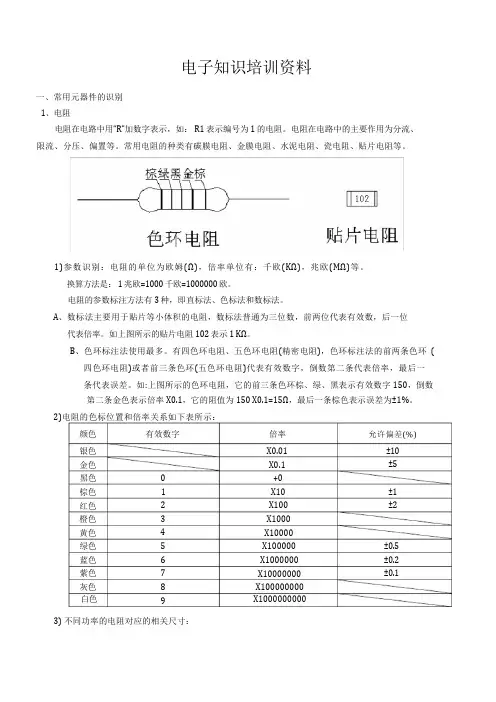
电子知识培训资料一、常用元器件的识别1、电阻电阻在电路中用“R”加数字表示,如: R1 表示编号为 1 的电阻。
电阻在电路中的主要作用为分流、限流、分压、偏置等。
常用电阻的种类有碳膜电阻、金膜电阻、水泥电阻、瓷电阻、贴片电阻等。
1)参数识别:电阻的单位为欧姆(Ω),倍率单位有:千欧(KΩ),兆欧(MΩ)等。
换算方法是: 1 兆欧=1000 千欧=1000000 欧。
电阻的参数标注方法有 3 种,即直标法、色标法和数标法。
A、数标法主要用于贴片等小体积的电阻,数标法普通为三位数,前两位代表有效数,后一位代表倍率。
如上图所示的贴片电阻 102 表示1 KΩ。
B、色环标注法使用最多。
有四色环电阻、五色环电阻(精密电阻),色环标注法的前两条色环 (四色环电阻)或者前三条色环(五色环电阻)代表有效数字,倒数第二条代表倍率,最后一条代表误差。
如:上图所示的色环电阻,它的前三条色环棕、绿、黑表示有效数字 150,倒数第二条金色表示倍率 X0.1,它的阻值为150 X0.1=15Ω,最后一条棕色表示误差为±1%。
2)电阻的色标位置和倍率关系如下表所示:颜色有效数字倍率允许偏差(%)银色X0.01 ±10金色X0.1 ±5黑色0 +0棕色 1 X10 ±1红色 2 X100 ±2橙色 3 X1000黄色 4 X10000绿色 5 X100000 ±0.5蓝色 6 X1000000 ±0.2紫色7 X10000000 ±0.1灰色8 X100000000白色9X10000000003) 不同功率的电阻对应的相关尺寸:尺寸功率ФD±0.5mm1/8W 1/4W 1/2W 1W 2W 3W5W4)贴片电阻各类参数L(mm) ±0.21.01.62.0 1/8W 、1/4W2、电容1) 电容在电路中普通用“C ”加数字表示(如C13 表示编号为 13 的电容)。


实用文档1.0 目的制订本指南﹐规公司的各层工作人员认识及辩别日常工作中常用的各类组件.2.0 围公司主要产品(计算机主板)中的电子组件认识:2.1工作中最常用的电子组件有﹕电阻﹑电容﹑电感﹑晶体管(包括二极管﹑发光二极管及三极管)﹑晶体﹑晶振(振荡器)和集成电路(IC)。
2.2 连接器件主要有﹕插槽﹑插针﹑插座等。
2.3 其它一些五金塑料散件﹕散热片﹑胶钉﹑跳线铁丝等。
3.0 责任3.1 公司的各层工作人员﹐正确认识及辩别日常操作中常用的各类组件﹐结合产品BOM的学习并应掌握以下基础知识或容﹕A) 从外观就能看出该组件的种类﹐名称以及是否有极性(方向性)。
B) 从组件表面的标记就能读出该组件的容量﹐允许误差围等参数。
C) 能辩识各类组件在线路板上的丝印图。
D) 知道在作业过程中不同组件需注意的事项。
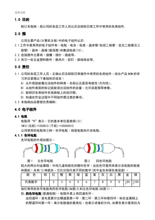
3.2 本指南由品管部负责编制;4.0 电子组件4.1 电阻电阻用“R”表示﹐它的基本单位是奥姆(Ω)1MΩ(兆欧)=1000KΩ(千欧)=1000000Ω公司常用的电阻有三种﹕色环电阻﹑排型电阻和片状电阻。
4.1.1 色环电阻色环电阻的外观如图示﹕图1 五色环电阻图2 四色环电阻较大的两头叫金属帽﹐中间几道有颜色的圈叫色环﹐这些色环是用来表示该电阻的阻值和围的﹐共有12种颜色﹐它们分别代表不同的数字(其中金色和银色表误差)﹕颜色棕红橙黄绿蓝紫灰白黑金银代表数字 1 2 3 4 5 6 7 8 9 0 +5% +10%我们常用的色环电阻有四色环电阻(如图2)和五色环电阻(如图1)﹕1).四色环电阻(普通电阻)﹕电阻外表上有四道色环﹕这四道环﹐首先是要分出哪道是第一环﹑第二环﹑第三环和第四环﹕标在金属帽上的那道环叫第一环﹐表示电阻值的最高位﹐也表示读值的方向。
如黄色表示最高位为四﹐紧挨第一环的叫第二环﹐表示电阻值的次高位﹐如紫色表示次高位为7﹔紧挨第2环的叫第3环﹐表示次高位后“0”的个数,如橙色表示后面有3个0﹔最后一环叫第4环﹐表示误差围﹐一般仅用金色或银色表示﹐如为金色﹐则表示误差围在+5%之间﹐如为银色﹐则表示误差围在+10%之间。
电子元器件有哪些?内容来源网络,由“深圳机械展(11万㎡,1100多家展商,超10万观众)”收集整理!更多cnc加工中心、车铣磨钻床、线切割、数控刀具工具、工业机器人、非标自动化、数字化无人工厂、精密测量、数控系统、3D打印、激光切割、钣金冲压折弯、精密零件加工等展示,就在深圳机械展.电子元器件是电子元件和电小型的机器、仪器的组成部分,其本身常由若干零件构成,可以在同类产品中通用;常指电器、无线电、仪表等工业的某些零件,如电容、晶体管、游丝、发条等子器件的总称。
常见的有二极管等。
电子元器件包括:电阻、电容器、电位器、电子管、散热器、机电元件、连接器、半导体分立器件、电声器件、激光器件、电子显示器件、光电器件、传感器、电源、开关、微特电机、电子变压器、继电器、印制电路板、集成电路、各类电路、压电、晶体、石英、陶瓷磁性材料、印刷电路用基材基板、电子功能工艺专用材料、电子胶(带)制品、电子化学材料及部品等。
电子元器件在质量方面国际上有欧盟的CE认证,美国的UL认证,德国的VDE和TUV以及中国的CQC认证等国内外认证,来保证元器件的合格。
概述一、元件:工厂在加工时没改变原材料分子成分的产品可称为元件,元件属于不需电子元器件要能源的器件。
它包括:电阻、电容、电感。
(又称为被动元件Passive Components)元件分为:1、电路类元件:二极管,电阻器等等2、连接类元件:连接器,插座,连接电缆,印刷电路板(PCB)二、器件:工厂在生产加工时改变了原材料分子结构的产品称为器件器件分为:1、主动器件,它的主要特点是:(1)自身消耗电能(2)需要外界电源。
2、分立器件,分为(1)双极性晶体三极管(2)场效应晶体管(3)可控硅(4)半导体电阻电容电阻电阻在电路中用"R”加数字表示,如:R1表示编号为1的电阻.电阻在电路中的主要作用为:分流、限流、分压、偏置等.电容电容在电路中一般用"C"加数字表示(如C13表示编号为13的电容).电容是由两片金属膜紧靠,中间用绝缘材料隔开而组成的元件.电容的特性主要是隔直流通交流.电容的容量大小表示能贮存电能的大小,电容对交流信号的阻碍作用称为容抗,它与交流信号的频率和电容量有关.晶体二极管晶体二极管在电路中常用“D”加数字表示,如: D5表示编号为5的二极管.作用:二极管的主要特性是单向导电性,也就是在正向电压的作用下,导通电阻很小;而在反向电压作用下导通电阻极大或无穷大.因为二极管具有上述特性,无绳电话机中常把它用在整流、隔离、稳压、极性保护、编码控制、调频调制和静噪等电路中.电感器电子元器件电感器在电子制作中虽然使用得不是很多,但它们在电路中同样重要。
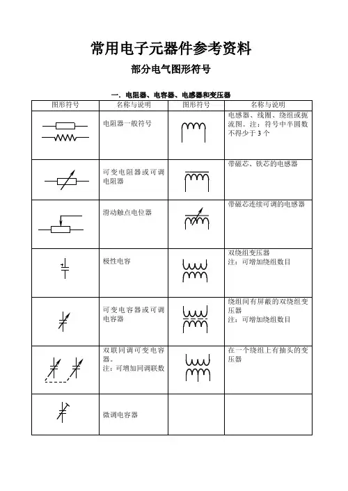
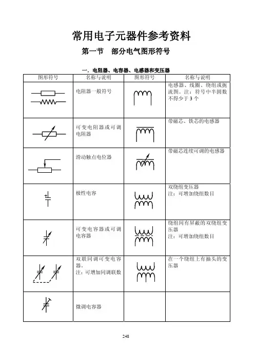
常用电子元器件参考资料部分电气图形符号一.电阻器、电容器、电感器和变压器二.半导体管三.其它电气图形符号常用电子元器件型号命名法及主要技术参数一.电阻器和电位器1.电阻器和电位器的型号命名方法示例:(1)精密金属膜电阻器R J7 3第四部分:序号第三部分:类别(精密)第二部分:材料(金属膜)第一部分:主称(电阻器)(2) 多圈线绕电位器W X D 3第四部分:序号第三部分:类别(多圈)第二部分:材料(线绕)第一部分:主称(电位器)2.电阻器的主要技术指标(1) 额定功率电阻器在电路中长时间连续工作不损坏,或不显著改变其性能所允许消耗的最大功率称为电阻器的额定功率。
电阻器的额定功率并不是电阻器在电路中工作时一定要消耗的功率,而是电阻器在电路工作中所允许消耗的最大功率。
不同类型的电阻具有不同系列的额定功率,如表2所示。
(2) 标称阻值阻值是电阻的主要参数之一,不同类型的电阻,阻值范围不同,不同精度的电阻其阻值系列亦不同。
根据国家标准,常用的标称电阻值系列如表3所示。
E24、E12和E6系列也适用于电位器和电容器。
(3) 允许误差等级3.电阻器的标志内容及方法(1)文字符号直标法:用阿拉伯数字和文字符号两者有规律的组合来表示标称阻值,额定功率、允许误差等级等。
符号前面的数字表示整数阻值,后面的数字依次表示第一位小数阻值和第二位小数阻值,其文字符号所表示的单位如表5所示。
如1R5表示1.5Ω,2K7表示2.7kΩ,表5例如:RJ71-0.125-5k1-II允许误差±10%标称阻值(5.1kΩ)额定功率1/8W型号由标号可知,它是精密金属膜电阻器,额定功率为1/8W,标称阻值为5.1kΩ,允许误差为±10%。
(2)色标法:色标法是将电阻器的类别及主要技术参数的数值用颜色(色环或色点)标注在它的外表面上。
色标电阻(色环电阻)器可分为三环、四环、五环三种标法。
其含义如图1和图2所示。
标称值第一位有效数字标称值第二位有效数字标称值有效数字后0的个数允许误差图1 两位有效数字阻值的色环表示法三色环电阻器的色环表示标称电阻值(允许误差均为±20%)。
FEATURESGreen-Mode PWMSupports the “Blue Angel” Standard Low Start-up Current (5uA) Low Operating Current (2mA) Leading-Edge BlankingConstant Output Power Limit Universal InputBuilt-in Synchronized Slope Compensation Current Mode OperationCycle-by-cycle Current Limiting Under Voltage Lockout (UVLO) Programmable PWM FrequencyGate Output Voltage Clamped at 15V Low CostFew External Components Required Small SOT-26 PackageAPPLICATIONSGeneral-purpose switching mode power supplies and flyback power converters, such asBattery chargers for cellular phones, cordless phones,PDAs, digital cameras, and power toolsPower adapters for ink jet printers, video gameconsoles, and portable audio playersOpen-frame SMPS for TV/DVD standby and otherauxiliary supplies, home appliances, and consumer electronicsReplacements for linear transformers and RCCSMPSPC 5V standby power.DESCRIPTIONThis highly-integrated PWM controller provides several special enhancements designed to meet the low standby-power needs of low-power SMPS. To minimize standby power consumption, the proprietary green-mode function provides off-time modulation to linearly decrease the switching frequency under light-load conditions. This green-mode function enables the power supply to easily meet even the strictest power conservation requirements.The BiCMOS fabrication process enables reducing the start-up current to 5uA, and the operating current to 2mA. To further improve power conservation, a large start-up resistance can be used. Built-in synchronized slope compensation ensures the stability of peak current mode control. Proprietary internal compensation provides a constant output power limit over a universal AC input range (90VAC to 264VAC). Pulse-by-pulse current limiting ensures safe operation even during short-circuits. To protect the external power MOSFET from being damaged by supply over voltage, the SG6848’s output driver is clamped at 15V. SG6848 controllers can be used to improve the performance and reduce the production cost of power supplies. The SG6848 is the best choice for replacing linear and RCC-mode power adapters. It is available in 8-pin DIP and 6-pin SOT-26 packages.TYPICAL APPLICATIONFrom auxiliary windingFBOUTPUTSENSERIGNDVDDSG6848R IN 1.5M R7100R S 4.7C6 472pR9 95kFrom bridge rectifier 120~380VDCC IN 10uMARKING DIAGRAMS PIN CONFIGURATIONORDERING INFORMATIONPart NumberPWM FrequencyPackageSG6848T 70kHz 6-Pin SOT-26 SG6848D 70kHz8-pin DIP-8PIN DESCRIPTIONSPin No.NameDIP-8 / (SOT-26)Type FunctionGATE 1 / (6) Driver Output The totem-pole output driver for driving the power MOSFET. VDD2 / (5)Supply Power supply. NC 3 NC pin.SENSE4 / (4)Analog InputCurrent sense. This pin senses the voltage across a resistor. When the voltage reaches the internal threshold, PWM output is disabled. This activates over-current protection. This pin also provides current amplitude information for current-mode control.RI 5 / (3)Analog Input/OutputA resistor connected from the RI pin to ground will generate a constant current source for the SG6848. This current is used to charge an internal capacitor, to determine the switching frequency. Increasing the resistance will reduce the amplitude of the current source and reduce the switching frequency. A 95k Ω resistor R i results in a 50uA constant current I i and a 70kHz switching frequency. NC 6 NC pin.FB 7 / (2) Analog Input Feedback. The FB pin provides the output voltage regulation signal. It provides feedback to the internal PWM comparator, so that the PWM comparator can control the duty cycle.GND8 / (1)SupplyGround.M : Mask VersionY : Year; WW : Work Week12345 6 SOT-26GND FBRIGATE VDD SENSE1 M A YWWXXXXXXX : Wafer Lot YY : Year; WW : Week V : Assembly Location81SG6848DXXXXXXXYYWWVDIP-8RINC FB GND SENSENCVDD GATE 4321 56 7 8BLOCK DIAGRAMV DD 2 (5)RI UVLO 16.3V/11.7VInternal Bias_+OSC 5 (3)RQ S OCP CompPWM CompSlopeCompensation Vlimit rampGreen Mode ControllerON/OFF Driver7 (2)4.8VFB1 (6)V DDSENSE4 (4)GATEBlanking Circuit8 (1)GNDABSOLUTE MAXIMUM RATINGSSymbol ParameterValueUnitV DDDC Supply Voltage * Zener Clamp Zener Current25 26 10 V V mA V FB Input Voltage to FB Pin -0.3 to 6 V V V Sense Input Voltage to Sense Pin -0.3 to 6V VP d Power Dissipation300 mW T J Operating Junction Temperature 150℃ SOT-26 208.4 °C/W R θJA Thermal Resistance (Junction to Air) DIP-8 82.5°C/W T stg Storage Temperature Range -55 to +150 ℃ T L Lead Temperature (Soldering) 20 sec SOT-2610 sec DIP-8220 260 °C ESD Capability, HBM Model 3.0 kVESD Capability, Model300V* All voltage values, except differential voltages, are given with respect to the network ground terminal.Low Cost Green-Mode PWM Controller for Flyback Converters SG6848RECOMMENDED OPERATING CONDITIONSSymbol ParameterValueUnitV DD DC Supply Voltage≦20 VT aOperating Ambient Temperature-30 to +85℃ELECTRICAL CHARACTERISTICS (T A = 25°C , VDD=15V) Feedback Input SectionSymbol ParameterTest Condition Min. Typ. Max. UnitI oz Zero Duty Cycle Input Current 1.3 2.0 mA V opOpen Loop Voltage4.5VCurrent Sense SectionSymbol ParameterTest Condition Min. Typ. Max. UnitZ cs Input Impedance 10 k Ω T PD Delay to Output150 200 nsec V TH,FLTCurrent Limit Flatten Threshold Voltage1.0VV TH,VALLEY Current Limit Valley Threshold Voltage0.80 0.85 0.90 VOscillator SectionSymbol ParameterTest Condition Min. Typ. Max. UnitF osc FrequencyR I =95k Ω 65 70 75 kHz F osc-green Green-Mode Frequency R I =95k Ω 13 15 kHzI g Green-Mode FB Input Current1.16mAI nGreen-Mode Start Threshold FB Input Current I n = 0.3mA for a Maximum Duty Cycle 1 mA S g Green-Mode Modulation Slope R I =95k Ω 300 Hz/uA F dv Frequency Variation versus V DD Deviation V DD =12 to 20V 0.02 2 % F dtFrequency Variation versus Temp. DeviationT A =-30 to 85 ℃2%PWM SectionSymbol ParameterTest Condition Min. Typ. Max. UnitDC (MAX) Maximum Duty Cycle 70 75 80 % DC (MIN) Minimum Duty Cycle - 1 2 % BnkLeading-Edge Blanking Time250nsecOutput SectionSymbol ParameterTest Condition Min. Typ. Max. UnitV ol Output Voltage Low V DD =15V, I o =20mA 1.5 V V oh Output Voltage High V DD =15V, I o =20mA 8 V t r Rising TimeV DD =15V, C L =1nF 50 200 nsec t f Falling TimeV DD =15V, C L =1nF 30 150 nsec V CLAMPOutput Clamp VoltageV DD =20V15 17 VUnder Voltage Lockout SectionSymbol Parameter TestCondition Min. Typ. Max. Unit V TH(ON)Start Threshold Voltage T A=25°C 15.3 16.3 17.3 VV DD(min)Min. Operating Voltage T A=25°C 10.9 11.7 12.5 VTotal Standby Current SectionSymbol Parameter TestCondition Min. Typ. Max. UnitI DD ST Start-upCurrent V DD=15V530uAI DD OP Operating Supply Current V DD=15V 2 5 mATYPICAL CHARACTERISTICSStart-up Threshold Voltage (V TH(ON)) vsTem perature14.515.015.516.016.517.0-40-25-105203550658095110125TEMPERATURE (℃)V T H (O N ) (V )Min. Operating Voltage (V DD (min)) vsTemperature10.610.811.011.211.411.611.812.012.2-40-25-105203550658095110125TEMPERATURE (℃)V D D (m i n ) (V )Start-up Crrent (I DD ST ) vs Tem perature51015202530-40-25-105203550658095110125TEMPERATURE (℃)I D D S T (u A )PWM Oscillator Frequency (F OSC ) vsTem perature65.066.568.069.571.072.574.0-40-25-105203550658095110125TEMPERATURE (℃)F O S C (K H z )Frequency in green m ode (F OSC-green )vs Tem perature89101112131415-40-25-105203550658095110125TEMPERATURE (℃)F O S C -g r e e n (K H z )Max. Duty Cycle (DC (MAX)) vsTem perature7071727374757677787980-40-25-105203550658095110125TEMPERATURE (℃)D C (M A X ) (%)PWM Oscillator Frequency (FOSC) vs.FB010203040506070800.60.70.80.91.01.11.21.31.4FB (mA )F O S C (K H z )OPERATION DESCRIPTIONSG6848 devices integrate many useful designs into one controller for low-power switch-mode power supplies. The following descriptions highlight some of the features of the SG6848 series.Start-up CurrentThe start-up current is only 5uA. Low start-up current allows a start-up resistor with a high resistance and a low-wattage to supply the start-up power for the controller. A 1.5 MΩ, 0.25W, start-up resistor and a 10uF/25V V DD hold-up capacitor would be sufficient for an AC-to-DC power adapter with a wide input range (100V AC to 240V AC).Operating CurrentThe operating current has been reduced to 2mA. The low operating current results in higher efficiency and reduces the V cc hold-up capacitance requirement. Green-Mode OperationThe proprietary green-mode function provides off-time modulation to linearly decrease the switching frequency under light-load conditions. On-time is limited to provide stronger protection against brownouts and other abnormal conditions. The feedback current, which is sampled from the voltage feedback loop, is taken as the reference. Once the feedback current exceeds the threshold current, the switching frequency starts to decrease. This green-mode function dramatically reduces power consumption under light-load and zero-load conditions. Power supplies using the SG6848 can easily meet even the strictest regulations regarding standby power consumption.Oscillator OperationA resistor connected from the RI pin to ground will generate a constant current source for the SG6848. This current is used to charge an internal capacitor. The charge-time determines the internal clock speed and the switching frequency. Increasing the resistance will reduce the amplitude of the input current and reduce the switching frequency. A 95kΩ resistor R i results in a 50uA constant current I i and a 70kHz switching frequency. The relationship between R i and the switching frequency is:)(kHz)(kR6650IPWMfΩ=The range of the oscillation frequency is designed to be within 50kHz ~ 100kHz.Leading-Edge BlankingEach time the power MOSFET is switched on, a turn-on spike will inevitably occur at the sense-resistor. To avoid premature termination of the switching pulse, a 250 nsec leading-edge blanking time is built in. Conventional RC filtering can therefore be omitted. During this blanking period, the current-limit comparator is disabled and it cannot switch off the gate driver.Constant Output Power LimitWhen the SENSE voltage across the sense resistor R s reaches the threshold voltage (around 1.0V), the output GATE drive will be turned off following a short propagation delay t D. This propagation delay will introduce an additional current proportional to t D*V in/L p. The propagation delay is nearly constant regardless of the input line voltage V IN. Higher input line voltages will result in larger additional currents. At high input line voltages, the output power limit will be higher than at low input line voltages.To compensate for this output power limit variation across a wide AC input range, the threshold voltage is adjusted by adding a positive ramp. This ramp signal rises from 0.85V to 1.0V, and then flattens out at 1.0V. A smaller threshold voltage forces the output GATE drive to terminate earlier. This reduces the total PWM turn-on time and makes the output power equal to that of low line input. This proprietary internal compensation ensures a constant output power limit for a wide AC input voltage range (90VAC to 264VAC).Under Voltage Lockout (UVLO)The turn-on and turn-off thresholds of the SG6848 are fixed internally at 16.3V/11.7V. During start-up, the hold-up capacitor must be charged to 16.3V through the start-up resistor, so that the SG6848 will be enabled. The hold-up capacitor will continue to supply V DD until power can be delivered from the auxiliary winding of the main transformer. V DD must not drop below 11.7V during this start-up process. This UVLO hysteresis window ensures that hold-up capacitor will be adequate to supply V DD during start-up.Gate OutputThe SG6848 BiCMOS output stage is a fast totem pole gate driver. Cross conduction has been avoided to minimize heat dissipation, increase efficiency, and enhance reliability. The output driver is clamped by an internal 15V Zener diode in order to protect power MOSFET transistors against undesired over-voltage gate signals. Built-in Slope CompensationThe sensed voltage across the current sense resistor is used for current mode control and pulse-by-pulse current limiting. Built-in slope compensation will improve stability and prevent sub-harmonic oscillations due to peak-current mode control. The SG6848 has a synchronized, positively-sloped ramp built-in at each switching cycle. The slope of the ramp is:(max)33.0DutyDuty×Noise ImmunityNoise from the current sense or the control signal can cause significant pulse width jitter, particularly in continuous-conduction mode. While slope compensation helps alleviate these problems, further precautions should still be taken. Good placement and layout practices should be followed. Avoiding long PCB traces and component leads, locating compensation and filter components near the SG6848, and increasing the power MOS gate resistance is advised.REFERENCE CIRCUIT CircuitVOGNDR13C10R12+C9U3312R1D521D121R8Q1123C3U1123456GND FB RISENSEVDD GATE +C2F1L112D421R11C1R4U21243CX1R7-+BD11432R5T18573,41,2109L212C6R9+C4R10R6R3D221+C8CY1C7R14R2LNBOMReference ComponentReferenceComponentBD1BD 1A/500VL2 10uH 6mm CX1 (Optional) YC 472P/400V (Y1) Q1 MOSFET 1A/600V CY1 (Optional) YC 102P/400V (Y1) R1,R2 R 750K Ω 1206 C2 EC 10uF/400V 105℃ R4,R3 R 47K Ω 1206 C1 CC 103P/500V R5 R 47Ω 1206 C3 CC 1000P/500V R6 R 4.7Ω 1206 C4 EC 10u/50V R7 R 100Ω 0805 C6 CC 472P 0805 R8 R 10Ω 1206 C7 (Optional) CC 102P/100V 1206 R10 (Optional) R 10Ω 1206C8 EC 470u/10V 105℃ R9 R 100K Ω 0805 C9 EC 220u/10V 105℃ R11 R 100Ω 1/8W C10 CC 222P 0805 R12 R 33K Ω 0805 D1 Diode FRI07 R13 R 33K Ω 1/8W D2Diode FR102R14 R 4.7K Ω 0805 D4 Diode SB360 T1 EE-16 D5 (Optional) ZD 6.8V 0.5W U1 IC SG6848 (Green PWM IC) F1 R 1Ω/0.5W U2 PC817 L120mH 6*8mmU3TL431PACKAGE INFORMATION 8 PINS -- DIP (D)4185DE 1EeBA 1A 2Abb1Le°ΘDimensionsMillimeters Inches SymbolMin. Typ. Max. Min. Typ. Max.A 5.334 0.210A1 0.3810.015A23.175 3.302 3.429 0.125 0.130 0.135b 1.524 0.060 b1 0.457 0.018 D 9.017 9.271 10.160 0.355 0.365 0.400 E 7.620 0.300 E1 6.223 6.350 6.477 0.245 0.250 0.255 e 2.540 0.100L 2.921 3.302 3.810 0.115 0.130 0.150 e B 8.509 9.017 9.525 0.335 0.355 0.375 θ˚0˚7˚ 15˚0˚7˚ 15˚SOT-26 (S)1364Ee1E 1eD b A 2A 1AθθR1RL 2L1LθDetail ADetail Ac11DimensionsMillimeters Inches SymbolMin. Typ. Max. Min. Typ. Max.A 1.45 0.057 A1 0.15 0.006 A2 0.90 1.15 1.30 0.036 0.045 0.051 b 0.30 0.50 0.011 0.020 c0.080.22 0.0030.009D 2.90 0.114E 2.80 0.110 E1 1.60 0.063 e 0.95 0.037 e1 1.90 0.075 L0.30 0.45 0.60 0.020 0.018 0.024L1 0.60 0.024 L2 0.25 0.010 R 0.10 0.004 R1 0.100.25 0.004 0.010 θ˚ 0˚ 4˚8˚0˚4˚8˚θ1˚5˚ 10˚ 15˚ 5˚ 10˚ 15˚DISCLAIMERSLIFE SUPPORTSystem General’s products are not designed to be used as components in devices intended to support or sustain human life. Use of System General’s products in components intended for surgical implant into the body, or other applications in which failure of System General’s products could create a situation where personal death or injury may occur, is not authorized without the express written approval of System General’s Chief Executive Officer. System General will not be held liable for any damages or claims resulting from the use of its products in medical applications. MILITARYSystem General's products are not designed for use in military applications. Use of System General’s products in military applications is not authorized without the express written approval of System General’s Chief Executive Officer. System General will not be held liable for any damages or claims resulting from the use of its products in military applications.RIGHT TO MAKE CHANGESSystem General reserves the right to change this document and/or this product without notice. Customers are advised to consult their System General sales representative before ordering.This datasheet has been downloaded from:Free DownloadDaily Updated Database100% Free Datasheet Search Site100% Free IC Replacement Search SiteConvenient Electronic DictionaryFast Search SystemAll Datasheets Cannot Be Modified Without Permission。