XL1530原厂规格书(2014版)
- 格式:pdf
- 大小:184.84 KB
- 文档页数:9
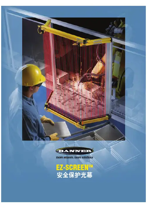
EZ-SCREEN TM2一种具备30mm 分辨率和15m 保护距离的低成本保护系统在危险低的区域保护采用EZ-SCREEN ®2级安全光幕,这是一种比较经济的解决方案。
危险低的环境是指意外事故的发生只会引起一些小的伤害,像肿伤、撞伤、跌伤、夹伤(但没有骨折)、割伤及擦伤。
具备30mm 的分辨率,可以检测小的物体,诸如手掌或脚踝,工作距离可达到15m ,具有广泛的应用。
符合二级的设计标准EZ-SCREEN ®2级满足抗震动、冲击试验、光性能及使用安全标准(IEC61496-1/-2与EN954-1)的二级应用的所有需求,具有连续的自诊断功能和外围设备控制的故障检测功能,是专为低危险程度保护而设计应用的,不建议用在手工危险操作的保护应用。
小巧、简单的两件式系统EZ-SCREEN ®2级是一种小巧的两件式系统,不需要单独的控制器,仅需包含了各自电源和光学同步功能的发射器和接收器即可,除去了DIP 开关功能选择或程序设定的调试功能,只要安装后就可使用。
可选手动或自动复位输出,响应速度快采用EZ-SCREEN ®2级,当遮挡光束消除时,需要自动复位输出可选择带T 的接收器型号,需要手动复位输出(如典型的安全门应用)可选择带L 的接收器型号。
优秀的2级设计具有极快的响应速度,11ms 到25ms 就可使设备迅速停机。
简单明了的诊断EZ-SCREEN ®2级具有非常明显的LED 状态指示灯:• 电源指示• 故障指示(LED 闪烁)• 顶部和底部光束接受指示• 光束或输出状态:遮挡或对准Trip 接收器Latch 接收器发射器3EZ-SCREEN 系统30mm 分辨率、8针M12(Euro 型)针式连接器接线的EZ-SCREEN 二级安全光幕各型号如下:单件或成对采购都可EZ-SCREEN 二级电缆4EZ-SCREEN TM 2级系统套装型号解析安全继电器模块EZ-SCREEN ®2级系统,可以单独购买,成对购买或套装购买,套装型号解析请看以下图示。
铝合金制品规格书1. 引言铝合金制品规格书是指对铝合金制品的各项技术要求、性能指标、检验方法等进行详细描述的文件。
本规格书旨在确保铝合金制品的质量,满足客户需求,并提供制造和检验的依据。
2. 适用范围本规格书适用于所有铝合金制品,包括但不限于铝合金型材、铝合金板材、铝合金管材等。
3. 规范引用在编写本规格书时,参考了以下标准和规范: - GB/T 3190-2010 铝及铝合金化学成分 - GB/T 3880-2012 铝及铝合金板材 - GB/T 6892-2006 铝及铝合金挤压型材- GB/T 5237.1-2008 铝型材表面处理4. 术语和定义4.1 铝合金制品指以铝为主要成分,添加其他元素而形成的具有特定性能和用途的产品。
4.2 型号根据不同的标准或客户要求,对不同种类的铝合金制品进行分类和命名的编号。
4.3 规格指铝合金制品的尺寸、形状、工艺要求等详细描述。
4.4 抗拉强度指铝合金制品在拉伸试验中最大承受的力,单位为兆帕(MPa)。
5. 技术要求5.1 化学成分铝合金制品的化学成分应符合GB/T 3190-2010标准中规定的要求。
5.2 物理性能铝合金制品的物理性能应符合以下要求: - 密度:不大于2.8 g/cm³; - 热膨胀系数:在20℃至100℃范围内,不大于24×10^-6/℃; - 硬度:根据型号和用途确定; - 弯曲强度:根据型号和用途确定。
5.3 表面处理铝型材表面处理应符合GB/T 5237.1-2008标准中规定的要求,常见表面处理方法包括氧化、喷砂、阳极氧化等。
5.4 尺寸和公差铝合金制品的尺寸和公差应符合相关标准或客户要求。
具体尺寸和公差范围可参考GB/T 3880-2012和GB/T 6892-2006标准。
5.5 表面质量铝合金制品的表面应平整、光洁,不得有明显的划痕、气泡、裂纹等缺陷。
具体要求可根据型号和用途确定。
5.6 抗拉强度铝合金制品的抗拉强度应符合相关标准或客户要求。

MBR1530CT - MBR1560CT15A SCHOTTKY BARRIER RECTIFIERFeaturesPin 1Pin 3Pin 2Maximum Ratings and Electrical Characteristics@ T A = 25°C unless otherwise specified·Schottky Barrier Chip·Guard Ring Die Construction for Transient Protection·Low Power Loss, High Efficiency ·High Surge Capability·High Current Capability and Low Forward Voltage Drop ·For Use in Low Voltage, High Frequency Inverters, Free Wheeling, and Polarity Protection Applications ·Lead Free Finish, RoHS Compliant (Note 3)Mechanical Data·Case: TO-220AB·Case Material: Molded Plastic. UL Flammability Classification Rating 94V-0·Moisture Sensitivity: Level 1 per J-STD-020C ·Terminals: Finish – Bright Tin. Solderable per MIL-STD-202, Method 208·Polarity: As Marked on Body ·Marking: Type Number ·Weight: 2.24 grams (approx.)Single phase, half wave, 60Hz, resistive or inductive load.For capacitive load, derate current by 20%.Notes:1. Thermal resistance junction to case mounted on heatsink.a2. Measured at 1.0MHz and applied reverse voltage of 4.0V DC.3.RoHS revision 13.2.2003. Glass and High Temperature Solder Exemptions Applied, see EU Directive Annex Notes 5 and 7.0.11.010500.20.40.60.81.0I ,I N S T A N T A N E O U S F W D C U R R E N T (A )F V ,INSTANTANEOUS FORWARD VOLTAGE (V)Fig.2Typical Forward CharacteristicsF050100150200250300110100I ,P E A K F O R W A R D S U R G E C U R R E N T (A )F S M NUMBER OFCYCLES AT 60HzFig.3Max Non-Repetitive Surge Current100100040000.11.010100C ,C A P A C I T A N C E (p F )T V ,REVERSE VOLTAGE (V)Fig.4Typical Total Capacitance (per element)R 0.0010.010.11.01020406080100120140I ,I N S T A N T A N E O U S R E V E R S E C U R R E N T (m A )R PERCENT OF RATED PEAK REVERSE VOLTAGE (%)Fig.5Typical Reverse Characteristics04850100150I ,A V E R A G E F O R W A R D C U R R E N T(A )(A V )T ,CASE TEMPERATURE (C)Fig.1Forward Current Derating CurveC °121620Ordering Information(Note 4)Notes: 4. For Packaging Details, go to our website at /datasheets/ap02007.pdf.分销商库存信息:DIODESMBR1530CT MBR1535CT MBR1540CT MBR1545CT MBR1550CT MBR1560CT。
MAX15301是一个全功能,高效,数字化的点负载(POL)操纵器与先进的电源治理和遥测功能与PID 为基础的数字电源稳压器,MAX15301采纳Maxim拥有专利的Intune的™自动补偿,状态空间操纵算法。
Intune 的操纵律是有效的小信号和大信号响应,占占空比饱和度的阻碍。
这排除需要用户以确信和设置的阈值从线性转换到非线性模式。
这些能力在快速环路的瞬态响应,并减少输出电容器的数量相较,竞争的模拟和数字操纵器。
MAX15301包括多种功能,以优化效率。
内部开关BabyBuck的稳压器可产生栅极驱动器和内部偏置电源,低功耗的操纵器。
一种先进的,高效率的MOSFET的栅极驱动器,具有自适应非重叠按时,而持续调整的高侧和低侧的按时和驱动电压的全范围内的电压,电流和温度,以尽可能减少开关损耗。
MAX15301设计最终客户的设计环境的初衷。
上的PMBus™兼容的串行总线接口进行通信的监控器监控和故障治理。
全套的电源治理功能,无需复杂和昂贵的测序和监控IC。
大体的DC-DC转换操作,可设置通过引脚搭接,并非需要用户配置固件。
这使得电源子系统的快速进展前完成板级系统的工程。
Maxim提供支持的硬件和软件配置MAX15301 ,MAX15301可在32引线,5mm×5mm TQFN封装,工作在-40°C至+85°C的温度范围内。
特点:的自动补偿功能能够确保稳固,同时优化瞬态性能2.在快速瞬态响应减少输出电容的非线性补偿结果3.差分远端电压传感许诺±1%V OUT精度在整个温度范围内(-40°C至+85°C)接口用于配置,操纵和监测5.支持电压定位6.提高效率(自适应非重叠时序驱动器)至14V的宽输入电压范围8.高效片上BabyBuck稳压器的自偏置9.输出电压范围从到10.进入预偏置输出启动11.可配置的软启动和软停止时刻12.固定工作频率同步(300kHz至1MHz)13.灵活的排序和故障治理14.引脚手动跳线配置(输出电压,从机地址,开关频率,电流限制)15.能够快速原型图表典型工作电路引脚名字功能1SYNC外部开关频率同步输入端。
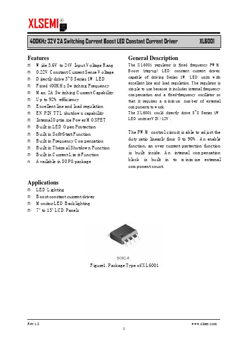
400KHz 32V 2A Switching Current Boost LED Constant Current Driver XL6001Featuresn Wide 3.6V to 24V Input Voltage Rang n0.22V Constant Current Sense Voltage n Directly drive 3~8 Series 1W LEDn Fixed 400KHz Switching Frequency n Max. 2A Switching Current Capability n Up to 92% efficiencyn Excellent line and load regulationn EN PIN TTL shutdown capabilityn Internal Optimize Power MOSFETn Built in LED Open Protectionn Built in Soft-Start Functionn Built in Frequency Compensationn Built in Thermal Shutdown Function n Built in Current Limit Functionn Available in SOP8 package Applicationsn LED Lightingn Boost constant current drivern Monitor LED Backlightingn7’ to 15’ LCD Panels General DescriptionThe XL6001 regulator is fixed frequency PWM Boost (step-up) LED constant current driver, capable of driving Series 1W LED units with excellent line and load regulation. The regulator is simple to use because it includes internal frequency compensation and a fixed-frequency oscillator so that it requires a minimum number of external components to work.The XL6001 could directly drive 5~8 Series 1W LED units at VIN>12V .The PWM control circuit is able to adjust the duty ratio linearly from 0 to 90%. An enable function, an over current protection function is built inside. An internal compensation block is built in to minimize external component count.Figure1. Package Type of XL6001400KHz 32V 2A Switching Current Boost LED Constant Current DriverXL6001Pin ConfigurationsSWEN FB VIN NCSW GNDGNDFigure2. Pin Configuration of XL6001 (Top View)Table 1 Pin DescriptionPin NumberPin Name Description1 ENEnable Pin. Drive EN pin low to turn off the device, drive ithigh to turn it on. Floating is default high.2 VINSupply V oltage Input Pin. XL6001 operates from a 3.6V to 24V DC voltage. Bypass Vin to GND with a suitably large capacitor to eliminate noise on the input.3 FB Feedback Pin (FB). The feedback threshold voltage is 0.22V .4 NC No Connected.5,6 SWPower Switch Output Pin (SW). Output is the switch node thatsupplies power to the output.7,8 GND Ground Pin.400KHz 32V 2A Switching Current Boost LED Constant Current Driver XL6001 Function BlockFigure3. Function Block Diagram of XL6001Typical Application CircuitFigure4. XL6001 Typical Application Circuit400KHz 32V 2A Switching Current Boost LED Constant Current Driver XL6001Ordering InformationPart Number Marking ID Lead Free Lead Free Packing Type XL6001E1 XL6001E1 Tube PackageTemperature RangeXL6001TRE1XL6001E1Tape & ReelXLSEMI Pb-free products, as designated with “E1” suffix in the par number, are RoHS compliant.Absolute Maximum Ratings (Note1)ParameterSymbol Value Unit Input VoltageVin -0.3 to 26 V Feedback Pin Voltage V FB -0.3 to Vin V EN Pin VoltageV EN -0.3 to Vin V Output Switch Pin Voltage V Output -0.3 to 32 V Power DissipationP D Internally limitedmW Thermal Resistance (SOP8)(Junction to Ambient, No Heatsink, Free Air) R JA 100 ºC/W Operating Junction Temperature T J -40 to 125 ºC Storage TemperatureT STG -65 to 150 ºC Lead Temperature (Soldering, 10 sec) T LEAD 260 ºC ESD (HBM)>2000VNote1: Stresses greater than those listed under Maximum Ratings may cause permanent damage to the device. This is a stress rating only and functional operation of the device at these or any other conditions above those indicated in the operation is not implied. Exposure to absolute maximum rating conditions for extended periods may affect reliability.400KHz 32V 2A Switching Current Boost LED Constant Current Driver XL6001 XL6001 Electrical CharacteristicsT a = 25℃;unless otherwise specified.Symbol Parameter Test Condition Min. Typ. Max. Unit System parameters test circuit figure4VFB FeedbackV oltageVin = 5V to 12V, V out=24VIload=100mA209 220 231 mVEfficiency ŋVin=12V ,V out= 6*1W LEDIout=0.3A- 92 - %Electrical Characteristics (DC Parameters)Vin = 12V, GND=0V, Vin & GND parallel connect a 47uf/25V capacitor; Iout=50mA, T a = 25℃; the others floating unless otherwise specified.Parameters Symbol Test Condition Min. Typ. Max. Unit Input operation voltage Vin 3.6 24 V Shutdown Supply Current I STBY V EN=0V 70 100 uAQuiescent Supply Current I q V EN =2V,V FB =Vin2.5 5 mAOscillator Frequency Fosc 320 400 480 Khz Switch Current Limit I L V FB =0 2 AOutput Power NMOS Rdson Vin=12V,I SW=2A110 120 mohmEN Pin Threshold V EN High (Regulator ON)Low (Regulator OFF)1.40.8VI H V EN =2V (ON) 3 10 uA EN Pin Input LeakageCurrent ILV EN =0V (OFF) 3 10 uA Max. Duty Cycle D MAX V FB=0V 90 %400KHz 32V 2A Switching Current Boost LED Constant Current Driver XL6001Schottky Diode Selection TableCurrent SurfaceMountThrough Hole VR (The same as system maximum input voltage)20V 30V 40V 50V60V1A √1N5817 1N5818 1N5819√ 1N5820 1N5821 1N5822√ MBR320 MBR330 MBR340 MBR350 MBR360 √ SK32 SK33 SK34SK35SK36 √ 30WQ03 30WQ04 30WQ05 √ 31DQ03 31DQ04 31DQ05 3A√SR302SR303SR304SR305SR306Typical System Application for VIN=5V to driver 2~6 x 1W series LED unitsFigure5. XL6001 System Parameters Test Circuit (2~6 x 1W LED)400KHz 32V 2A Switching Current Boost LED Constant Current Driver XL6001 Typical System Application for VIN=12V to driver 4~8 x 1W series LED unitsFigure6. XL6001 System Parameters Test Circuit (4~8 x 1W LED)Typical System Application for VIN=12V to driver 4~8 x 1W series LED units With PWM DimmingFigure7. XL6001 System Parameters Test Circuit (4~8 x 1W LED with PWM Dimming)400KHz 32V 2A Switching Current Boost LED Constant Current Driver XL6001 Typical System Application for SEPIC Buck-Boost LED DriverFigure8. XL6001 System Parameters Test Circuit (Buck-Boost LED Driver)400KHz 32V 2A Switching Current Boost LED Constant Current Driver XL6001 Package InformationSOP8 Package Mechanical Dimensions。

电动订书机产品规格书
1、适用范围
本规格书适用于DXC公司生产的电动订书机。
2、定义
2.1电动订书机:当纸触发入纸口感应开关时,通过线线路和机械联动,在
要求位置打钉的装置。
2.2正常电压:对额定电压120VAC/60Hz为120VAC/60Hz;对额定电压
220~240VAC/50Hz为230 VAC/50Hz。
2.3低电压:对额定电压120VAC/60Hz为105VAC/60Hz;对额定电压
220~240VAC/50Hz为198 VAC/50Hz。
2.4高电压:对额定电压120VAC/60Hz为130VAC/60Hz;对额定电压
220~240VAC/50Hz为264 VAC/50Hz。
3、产品规格
3.1特性/参数
3.2外观与颜色
--外观、颜色不可有明显的缺点,如脱色、凹陷、裂痕及脏污;
--印有指示应正确、及印于规定位置;
--外壳应光滑,不能有利边,且段差小于0.3mm;
--外观型状与结构图相符,如不能以结构图作出评定标准,则与“可接收”样板相符;
--详细颜色参考《YRS309BOM》。
3.3主要部件材质
3.4标识。
目录1.用户注意事项 (2)安全提示 (2)注意事项 (2)2.机器安装与调校 (2)2.1工作环境及条件 (2)2.2机器安装 (2)2.3机器调校 (3)2.4装箱清单 (3)3.机器说明书 (3)3.1概述 (3)3.2主要技术参数 (4)3.3机器工作流程 (4)3.4机器操作说明 (5)3.4.1通电前检查 (5)3.4.2确定贴装方式及数量 (6)3.4.3调节头部及飞达间距 (6)3.4.4调节吸嘴及飞达间距 (11)3.4.5贴装程序 (13)3.4.6做MARK点 (19)3.5常见问题与处理 (22)4.电气控制电路图 (24)4.1 电箱布局图 (24)4.2电路控制图 (25)5、维护与保养 (32)5.1吸嘴保养 (32)5.2飞达工作台保养 (34)5.3导轨和丝杆保养 (34)5.4飞达维修与保养 (35)5.5真空泵维护与保养 (37)6.机器保修信息 (39)6.1保修卡 (39)6.2维修记录卡 (41)7.售后服务信息 (42)1.用户注意事项感谢您使用深圳市易通自动化机器有限公司生产的H T1530系列L E D贴片机!安全提示:● 本机器只能由专业维护及维修人员或培训合格的人员进行操作● 通电之前,应确认外接输入电源与该机器的额定电压及电流相符● 本机器内含运动装置及机械传动,操作时应注意人身安全注意事项:●操作本机器前请仔细阅读本用户手册● 请不要把本机器安装在电磁干扰源附近● 请使用规定的电压、电流、功率(详见机器安装与调校)● 机器不使用时,请关闭电源、气源● 保养、维修之前,请关闭机器电源● 请按本手册要求定期对机器进行保养● 勿改变本机器电控箱内的软体及硬体设置● 请妥善保管本手册,以便维护保养及维修时查阅2.机器安装与调校2.1工作环境及条件1.本设备应放置在平坦坚固地面;2.工作环境温度应在22~28℃之间;3.工作环境湿度应在45~75RH%之间;4. 机器附近不能有强磁场;5. 使用具有三相AC380V(50-60HZ)稳定电压的电源(保证接地良好);6. 使用气源0.5~0.6MPa(气源为大气压霜点:-17℃以下,微粒粉:粒径5μm以下,最高油分浓度:5㎎/m以下)。
–1-17–耐热PVC双重绝缘电线Irradiated cross-linked PVC insulated wire设备内配线用电线Appliance wiring material1430 REW (XLPVC)1430 AWM●额定Rating 105℃, 300V●标准StandardUL Subject 758, CSA C22.2 No.127, No.210.2●日立标准规格书Hitachi Specification : SP23-90743■特长1.难燃性UL:VW-1,CSA:FT1电气用品安全法:-F-2.经辐射交联,对热稳定。
3.机械强度出色。
4.部分最小厚度在0.40mm以上,适用于欧洲。
■用途电气、电子设备的内部配线。
马达导线、照明器具接线和空调器配线等。
■构造和性能◆Features1.Flammability VW-1, FT1, –F–2.Excellent thermal stability due to irradiated cross-linked insulation.3.Excellent mechanical strength.4.With minimum thickness more than 0.40mm at any point, this wire is ideal for European markets.◆ApplicationInternal wiring for electric and electronic equipment.Motor lead wires, wiring of light fixtures, and air conditioners.◆Construction, Properties表面标识(例):AWM E41447 STYLE 1430 LF 26AWG 105C VW-1 HITACHI –F –CSA LL24713 TYPE REW (XLPVC) 105C 300V FT1Marking (ex.)(HITACHI-T)(LL48469)备注1.TASC:绞线整体镀锡导体2.电气特性最小绝缘电阻(15.6℃时):10M Ω-km 耐电压:A.C.2000V/1min.3. 许可导体型号范围:30~16AWG■品名略号(例)UL1430 AWM 1X28AWG (7/0.127) LFUL1430 REW (XLPVC) 1 ×26AWG (7/0.16) LF ■品名代码:141Note1.TASC : Hi-wrap wire2.Electrical propertiesMin. insulation resistance (at 15.6°C) : 10M Ω-km Dielectric withstanding voltage : A.C.2000V/1min.3.Size range : 30~16AWG◆ Ordering description (ex.)UL1430 AWM 1 × 28AWG (7/0.127) LFUL1430 REW (XLPVC) 1 × 26AWG (7/0.16)LF ◆ Product I.D. : 141。

60065(2014版)标准—说明书和标识NO.Item Verdict 标识符号1、(5.4.a) Where in a manufacturer's service documentation, for example in circuit diagrams orlists of components, a symbol is used to indicate that a specific component shall bereplaced only by the component specified in that documentation for safety reasons,the following symbol shall be used:,ISO 7000-0434 (2004-01)This symbol may also be put adjacent to the relevant component.This symbol shall not be placed on components.P N如果在制造厂商的维修文件中,例如在电路图或元器件表中要使用一种符号,用来表示某一特定的元器件由于安全的原因,只能用该文件中规定的元器件来更换,则应当使用下列符号:,ISO 7000-0434 (2004-01)该符号也可以标在有关元器件的附近。
该符号不得标在元器件上。
2、(5.4.b) Where a loudspeaker grille, removable from the outside by the use of a tool, coin orother object, is relied on as protective cover (see 9.2), the following marking, or equ-ivalent, shall be visible on the enclosure after removal of the grille:CAUTIONTo prevent electric shock hazard, do not connect tomains power supply while grille is removed.Alternatively, the symbol , IEC 60417-5036 (200210) shall be visible after removal of the grille and the caution wording above shall appear in the userinstructions, accompanied by the symbol.P N在一个扬声器格栅的地方,可从外部通过使用一种工具,像硬币或者其他对象作为一种防护罩来依靠,下列标志或者类似标志,在删除格栅后,应该在外壳上清晰可见:警告为了防止点击危险,当格栅被删除时,不能连接到供电电源。
Dimensions: [mm]Scale - 2,5:17447720101A74477201017447720101T e m p e r a t u r eT T T 7447720101Cautions and Warnings:The following conditions apply to all goods within the product series of WE-TI of Würth Elektronik eiSos GmbH & Co. KG:General:•This electronic component was designed and manufactured for use in general electronic equipment.•Würth Elektronik must be asked for written approval (following the PPAP procedure) before incorporating the components into any equipment in fields such as military, aerospace, aviation, nuclear control, submarine, transportation (automotive control, train control, ship control), transportation signal, disaster prevention, medical, public information network, etc. where higher safety and reliability are especially required and/or if there is the possibility of direct damage or human injury.•Electronic components that will be used in safety-critical or high-reliability applications, should be pre-evaluated by the customer. •The component is designed and manufactured to be used within the datasheet specified values. If the usage and operation conditions specified in the datasheet are not met, the wire insulation may be damaged or dissolved.•Do not drop or impact the components, the component may be damaged.•Würth Elektronik products are qualified according to international standards, which are listed in each product reliability report. Würth Elektronik does not warrant any customer qualified product characteristics beyond Würth Elektroniks’ specifications, for its validity and sustainability over time.•The customer is responsible for the functionality of their own products. All technical specifications for standard products also apply to customer specific products.Product specific:Soldering:•The solder profile must comply with the technical product specifications. All other profiles will void the warranty.•All other soldering methods are at the customers’ own risk.Cleaning and Washing:•Washing agents used during the production to clean the customer application might damage or change the characteristics of the wire insulation, marking or plating. Washing agents may have a negative effect on the long-term functionality of the product. Potting:•If the product is potted in the costumer application, the potting material might shrink or expand during and after hardening. Shrinking could lead to an incomplete seal, allowing contaminants into the core. Expansion could damage the components. We recommend a manual inspection after potting to avoid these effects. Storage Conditions:• A storage of Würth Elektronik products for longer than 12 months is not recommended. Within other effects, the terminals may suffer degradation, resulting in bad solderability. Therefore, all products shall be used within the period of 12 months based on the day of shipment.•Do not expose the components to direct sunlight.•The storage conditions in the original packaging are defined according to DIN EN 61760-2.•The storage conditions stated in the original packaging apply to the storage time and not to the transportation time of the components. Packaging:•The packaging specifications apply only to purchase orders comprising whole packaging units. If the ordered quantity exceeds or is lower than the specified packaging unit, packaging in accordance with the packaging specifications cannot be ensured. Handling:•Violation of the technical product specifications such as exceeding the nominal rated current will void the warranty.•Applying currents with audio-frequency signals might result in audible noise due to the magnetostrictive material properties. •Due to heavy weight of the components, strong forces and high accelerations might have the effect to damage the electrical connection or to harm the circuit board and will void the warranty.•Please be aware that products provided in bulk packaging may get bent and might lead to derivations from the mechanical manufacturing tolerances mentioned in our datasheet, which is not considered to be a material defect.•The temperature rise of the component must be taken into consideration. The operating temperature is comprised of ambient temperature and temperature rise of the component.The operating temperature of the component shall not exceed the maximum temperature specified.These cautions and warnings comply with the state of the scientific and technical knowledge and are believed to be accurate and reliable.However, no responsibility is assumed for inaccuracies or incompleteness.Würth Elektronik eiSos GmbH & Co. KGEMC & Inductive SolutionsMax-Eyth-Str. 174638 WaldenburgGermanyCHECKED REVISION DATE (YYYY-MM-DD)GENERAL TOLERANCE PROJECTIONMETHODTRi001.0012019-07-17DIN ISO 2768-1mDESCRIPTIONWE-TI Radial Leaded Wire WoundInductor ORDER CODE7447720101SIZE/TYPE BUSINESS UNIT STATUS PAGEImportant NotesThe following conditions apply to all goods within the product range of Würth Elektronik eiSos GmbH & Co. KG:1. General Customer ResponsibilitySome goods within the product range of Würth Elektronik eiSos GmbH & Co. KG contain statements regarding general suitability for certain application areas. These statements about suitability are based on our knowledge and experience of typical requirements concerning the areas, serve as general guidance and cannot be estimated as binding statements about the suitability for a customer application. The responsibility for the applicability and use in a particular customer design is always solely within the authority of the customer. Due to this fact it is up to the customer to evaluate, where appropriate to investigate and decide whether the device with the specific product characteristics described in the product specification is valid and suitable for the respective customer application or not.2. Customer Responsibility related to Specific, in particular Safety-Relevant ApplicationsIt has to be clearly pointed out that the possibility of a malfunction of electronic components or failure before the end of the usual lifetime cannot be completely eliminated in the current state of the art, even if the products are operated within the range of the specifications.In certain customer applications requiring a very high level of safety and especially in customer applications in which the malfunction or failure of an electronic component could endanger human life or health it must be ensured by most advanced technological aid of suitable design of the customer application that no injury or damage is caused to third parties in the event of malfunction or failure of an electronic component. Therefore, customer is cautioned to verify that data sheets are current before placing orders. The current data sheets can be downloaded at .3. Best Care and AttentionAny product-specific notes, cautions and warnings must be strictly observed. Any disregard will result in the loss of warranty.4. Customer Support for Product SpecificationsSome products within the product range may contain substances which are subject to restrictions in certain jurisdictions in order to serve specific technical requirements. Necessary information is available on request. In this case the field sales engineer or the internal sales person in charge should be contacted who will be happy to support in this matter.5. Product R&DDue to constant product improvement product specifications may change from time to time. As a standard reporting procedure of the Product Change Notification (PCN) according to the JEDEC-Standard inform about minor and major changes. In case of further queries regarding the PCN, the field sales engineer or the internal sales person in charge should be contacted. The basic responsibility of the customer as per Section 1 and 2 remains unaffected.6. Product Life CycleDue to technical progress and economical evaluation we also reserve the right to discontinue production and delivery of products. As a standard reporting procedure of the Product Termination Notification (PTN) according to the JEDEC-Standard we will inform at an early stage about inevitable product discontinuance. According to this we cannot guarantee that all products within our product range will always be available. Therefore it needs to be verified with the field sales engineer or the internal sales person in charge about the current product availability expectancy before or when the product for application design-in disposal is considered. The approach named above does not apply in the case of individual agreements deviating from the foregoing for customer-specific products.7. Property RightsAll the rights for contractual products produced by Würth Elektronik eiSos GmbH & Co. KG on the basis of ideas, development contracts as well as models or templates that are subject to copyright, patent or commercial protection supplied to the customer will remain with Würth Elektronik eiSos GmbH & Co. KG. Würth Elektronik eiSos GmbH & Co. KG does not warrant or represent that any license, either expressed or implied, is granted under any patent right, copyright, mask work right, or other intellectual property right relating to any combination, application, or process in which Würth Elektronik eiSos GmbH & Co. KG components or services are used.8. General Terms and ConditionsUnless otherwise agreed in individual contracts, all orders are subject to the current version of the “General Terms and Conditions of Würth Elektronik eiSos Group”, last version available at .Würth Elektronik eiSos GmbH & Co. KGEMC & Inductive SolutionsMax-Eyth-Str. 174638 WaldenburgGermanyCHECKED REVISION DATE (YYYY-MM-DD)GENERAL TOLERANCE PROJECTIONMETHODTRi001.0012019-07-17DIN ISO 2768-1mDESCRIPTIONWE-TI Radial Leaded Wire WoundInductor ORDER CODE7447720101SIZE/TYPE BUSINESS UNIT STATUS PAGE。
XLXL系列使用手冊著作權著作權所有 © 2017 年,BenQ Corporation。
所有權利均予保留。
未經BenQ Corporation 事前書面之許可,本文的任何部分皆不可以任何形式或任何方法,包括電子、機械、磁性、光學、化學、手寫或任何方式予以重製、傳輸、轉譯、儲存於檢索系統或翻譯成任何文字或電腦語言。
免責聲明對於本文之任何明示或暗示內容,BenQ Corporation不做任何保證,亦拒絕對任何特殊目的之商用性或適用性目的予以保證。
此外,BenQ Corporation保留修改或變更本文之權利,並且修改或變更內容將不另行通知。
不閃爍的效能表現,可能會受到諸多外在因素影響(例如訊號線品質不良、電源供應不穩、訊號干擾或接地不當),且並不侷限於以上述及的這些外在因素。
(僅適用於不閃爍的型號。
)BenQ ecoFACTSBenQ has been dedicated to the design and development of greener product as part of itsaspiration to realize the ideal of the "Bringing Enjoyment 'N Quality to Life" corporate vision with the ultimate goal to achieve a low-carbon society. Besides meeting international regulatory requirement and standards pertaining to environmental management, BenQ has spared noefforts in pushing our initiatives further to incorporate life cycle design in the aspects ofmaterial selection, manufacturing, packaging, transportation, using and disposal of the products.BenQ ecoFACTS label lists key eco-friendly design highlights of each product, hoping to ensure that consumers make informed green choices at purchase. Check out BenQ's CSR Website at / for more details on BenQ's environmental commitments andachievements.23電源安全說明•交流電插頭會將本設備與交流電電源隔離。
180KHz 60V 5A Switching Current Boost LED Constant Current Driver XL6006Featuresn Wide 5V to 32V Input Voltage Rangen Maximum Boost Output Up to 60Vn0.22V FB adjustable LED drive current n Directly drive 16 Series 1W/3W LED at VIN=24Vn Fixed 180KHz Switching Frequencyn Max. 5A Switching Current Capabilityn Up to 94% efficiencyn Excellent line and load regulationn EN PIN TTL shutdown capabilityn Internal Optimize Power MOSFETn Built in Soft-Start Functionn Built in Frequency Compensationn Built in Thermal Shutdown Functionn Built in Current Limit Functionn Available in TO263-5L & TO220-5L packageApplicationsn LED Lightingn Boost constant current drivern TFT LED Backlighting General DescriptionThe XL6006 regulator is fixed frequency PWM Boost (step-up) LED constant current driver, capable of driving Series 1W/3W/5W LED units with excellent line and load regulation. The regulator is simple to use because it includes internal frequency compensation and a fixed-frequency oscillator so that it requires a minimum number of external components to work.The XL6006 could directly drive 16 Series 1W/3W LED units at VIN=24V .The PWM control circuit is able to adjust the duty ratio linearly from 0 to 90%. An enable function, an over current protection function is built inside. An internal compensation block is built in to minimize external component count.Figure1. Package Type of XL6006180KHz 60V 5A Switching Current Boost LED Constant Current Driver XL6006 Pin ConfigurationsFigure2. Pin Configuration of XL6006 (Top View)Table 1 Pin DescriptionPin Number Pin Name Description1 GND Ground Pin.2 EN Enable Pin. Drive EN pin low to turn off the device, drive it high to turn it on. Floating is default high.3 SW Power Switch Output Pin (SW).4 VIN Supply V oltage Input Pin. XL6006 operates from a 5V to 32V DC voltage. Bypass Vin to GND with a suitably large capacitor to eliminate noise on the input.5 FB Feedback Pin (FB). The feedback threshold voltage is 0.22V.180KHz 60V 5A Switching Current Boost LED Constant Current DriverXL6006Function BlockFigure3. Function Block Diagram of XL6006Typical Application CircuitFigure4. XL6006 Typical Application Circuit180KHz 60V 5A Switching Current Boost LED Constant Current Driver XL6006Ordering InformationPart Number Marking ID Lead Free Lead Free Packing Type XL6006TE1 XL6006TE1 Tube PackageTemperature RangeXL6006SE1XL6006SE1Tape & ReelXLSEMI Pb-free products, as designated with “E1” suffix in the par number, are RoHS compliant.Absolute Maximum Ratings (Note1)ParameterSymbol Value Unit Input VoltageVin -0.3 to 36 V Feedback Pin Voltage V FB -0.3 to Vin V EN Pin VoltageV EN -0.3 to Vin V Output Switch Pin Voltage V Output -0.3 to 60 V Power DissipationP D Internally limitedmW Thermal Resistance (TO220-5L/TO263-5L) (Junction to Ambient, No Heatsink, Free Air) R JA 30 ºC/W Operating Junction Temperature T J -40 to 125 ºC Storage TemperatureT STG -65 to 150 ºC Lead Temperature (Soldering, 10 sec) T LEAD 260 ºC ESD (HBM)2000VNote1: Stresses greater than those listed under Maximum Ratings may cause permanent damage to the device. This is a stress rating only and functional operation of the device at these or any other conditions above those indicated in the operation is not implied. Exposure to absolute maximum rating conditions for extended periods may affect reliability.180KHz 60V 5A Switching Current Boost LED Constant Current Driver XL6006 XL6006 Electrical CharacteristicsT a = 25℃;unless otherwise specified.Symbol Parameter Test Condition Min. Typ. Max. Unit System parameters test circuit figure4VFB FeedbackV oltageVin = 5V to 12V, V out=24VIload=100mA209 220 231 mVEfficiency ŋVin=12V ,V out=51.2VIout=350mA- 92 - %Electrical Characteristics (DC Parameters)Vin = 12V, GND=0V, Vin & GND parallel connect a 100uf/50V capacitor; Iout=100mA, T a = 25℃; the others floating unless otherwise specified.Parameters Symbol Test Condition Min. Typ. Max. Unit Input operation voltage Vin 5 32 V Shutdown Supply Current I STBY V EN=0V 70 100 uAQuiescent Supply Current I q V EN =2V,V FB =Vin2.5 5 mAOscillator Frequency Fosc 144 180 216 KHz Switch Current Limit I L V FB =0 5 AOutput Power NMOS Rdson Vin=12V,I SW=5A35 40 mohmEN Pin Threshold V EN High (Regulator ON)Low (Regulator OFF)1.40.8VI H V EN =2V (ON) 3 10 uA EN Pin Input LeakageCurrent ILV EN =0V (OFF) 3 10 uA Max. Duty Cycle D MAX V FB=0V 90 %180KHz 60V 5A Switching Current Boost LED Constant Current Driver XL6006Schottky Diode Selection TableCurrent SurfaceMountThrough Hole VR (The same as system maximum input voltage)20V 30V 40V 50V 60V1A √1N5817 1N5818 1N5819√ 1N5820 1N5821 1N5822√ MBR320 MBR330 MBR340 MBR350 MBR360 √ SK32 SK33 SK34SK35SK36 √ 30WQ03 30WQ04 30WQ05 √ 31DQ03 31DQ04 31DQ05 3A√SR302SR303SR304SR305SR306√ 1N5823 1N5824 1N5825 √ SR502 SR503 SR504 SR505 SR506 √ SB520 SB530 SB540SB550SB560 5A√50WQ0350WQ04 50WQ05Typical System Application for VIN=12V to driver 16 x 1W series LED unitsFigure5. XL6006 System Parameters Test Circuit (12V ~16 x 1W LED)180KHz 60V 5A Switching Current Boost LED Constant Current Driver XL6006 Typical System Application for VIN=12V to driver 8 x 3W series LED unitsFigure6. XL6006 System Parameters Test Circuit (12V ~ 8 x 3W LED) Typical System Application for VIN=24V to driver 16 x 3W series LED unitsFigure7. XL6006 System Parameters Test Circuit (24V ~ 16 x 3W LED)180KHz 60V 5A Switching Current Boost LED Constant Current Driver XL6006Typical System Application for VIN=12V to driver 16 series x 40 parallelWhite LED ArrayFigure8. XL6006 System Parameters Test Circuit (12V ~ 16 x 40 White LED)Typical System Application for SEPIC Buck-Boost LED DriverOutput Drive series 8 1W/3W LEDFigure9. XL6006 System Parameters Test Circuit (Buck-Boost LED Driver)180KHz 60V 5A Switching Current Boost LED Constant Current Driver XL6006Typical System Application for VIN=12V to driver 16 x 1W series LED units With Dimming FunctionFigure10. XL6006 System Test Circuit (12V ~16 x 1W LED with Dimming Function)180KHz 60V 5A Switching Current Boost LED Constant Current Driver XL6006Package InformationTO220-5LDatasheet 180KHz 60V 5A Switching Current Boost LED Constant Current DriverXL6006Rev 1.4 11 Package InformationTO263-5L。
Output Voltage Change Vs Output CurrentEfficiency Vs Output Current 2. XL1530 12V 转 5V (负载 0.2A—3A )效率图和输出电压变化曲线:1. XL1530 12V 转 5V (负载 0.2A—3A )应用电路图:AV V 单位 0 to 353.6 to 18值IOUTVOUT VIN 符号输出电流输出电压 输入电压 参数一:XL1530 典型应用测试:XL1530 DEMO BOARD MANUAL反面正面XL1530PCB 图:大电流走线要粗,短,不拐弯反馈点要接到输出滤波电容 C2,COUT 之后输入电解电容 CIN ,陶瓷电容 C1 布局布线要紧靠芯片 7,8(GND )和 4(VIN )(1)流大电流的线要粗,短,不拐弯。
(2)7,8 脚(GND ) 脚(VIN )线要粗,短线,不拐弯,且输入电解电容 CIN 和 105 C1,4 陶瓷电容紧挨第 4 脚(VIN )和 7,8 脚(GND)。
(主要是为了减小输入电源布线寄生的电感, 电阻产生的高压开关毛刺干扰)(3)5,6 脚(SW )输出线要粗,短线,不拐弯,电感和续流二极管要紧挨第 5,6 脚(SW ) 输出端。
(4) 脚1 (FB )走线要接到输出滤波电容 C2,COUT 之后, PCB 布线远离 L1,D1,避免噪声干扰。
二:XL1530 PCB 板布局建议:三:XL1530 温度测试数据1:XL1530 电路图和 PCB 版图。
XL1530 温度测试点电感(L1)温度测试点输出电容(COUT )温度测试点肖特基二极管(D1)温度测试点输入电容(CIN )温度测试点2:XL1530 DEMO 板工作时(12V 转 5V )各元件温度,自然通风,室温:16℃。
输出负载电流 0.2A 2.5A 0.5A 1A 1.5A 2A 3A XL1530 电感(33uH/3A ) 20℃ 36℃ 47℃ 22℃25℃31℃63℃19℃ 29℃ 36℃ 21℃23℃26℃46℃肖特基二极管(IN5822) 19℃ 29℃ 35℃ 20℃22℃26℃38℃输入电容(35V/220uF ) 17℃ 26℃ 30℃ 18℃20℃22℃33℃输出电容(35V/220uF )18℃26℃30℃18℃19℃21℃34℃昆山东森微电子有限公司电话**************传真**************。