EMI电源滤波器220V/250V 单相双节伺服电源滤波器ME410-20A 交流增强型
- 格式:pdf
- 大小:1.19 MB
- 文档页数:12

常⽤替换运放型号对⽐常⽤替换运放型号对⽐CA3130 ⾼输⼊阻抗运算放⼤器 Intersil[DATA] CA3140 ⾼输⼊阻抗运算放⼤器 CD4573 四可编程运算放⼤器 MC14573ICL7650 斩波稳零放⼤器 LF347(NS[DATA]) 带宽四运算放⼤器 KA347 LF351 BI-FET单运算放⼤器 NS[DATA] LF353 BI-FET双运算放⼤器 NS[DATA] LF356 BI-FET单运算放⼤器 NS[DATA] LF357 BI-FET单运算放⼤器 NS[DATA] LF398 采样保持放⼤器 NS[DATA] LF411 BI-FET单运算放⼤器 NS[DATA] LF412 BI-FET双运放⼤器 NS[DATA] LM124 低功耗四运算放⼤器(军⽤档) NS[DATA]/TI[DATA] LM1458 双运算放⼤器 NS[DATA] LM148 四运算放⼤器 NS[DATA] LM224J 低功耗四运算放⼤器(⼯业档)NS[DATA]/TI[DATA] LM2902 四运算放⼤器 NS[DATA]/TI[DATA] LM2904 双运放⼤器 NS[DATA]/TI[DATA] LM301 运算放⼤器 NS[DATA] LM308 运算放⼤器 NS[DATA] LM308H 运算放⼤器(⾦属封装) NS[DATA] LM318 ⾼速运算放⼤器NS[DATA] LM324(NS[DATA]) 四运算放⼤器 HA17324,/LM324N(TI) LM348 四运算放⼤器 NS[DATA] LM358 NS[DATA] 通⽤型双运算放⼤器 HA17358/LM358P(TI) LM380 ⾳频功率放⼤器NS[DATA] LM386-1 NS[DATA] ⾳频放⼤器NJM386D,UTC386 LM386-3 ⾳频放⼤器 NS[DATA] LM386-4 ⾳频放⼤器 NS[DATA] LM3886 ⾳频⼤功率放⼤器 NS[DATA] LM3900 四运算放⼤器 LM725 ⾼精度运算放⼤器NS[DATA] LM733 带宽运算放⼤器 LM741 NS[DATA] 通⽤型运算放⼤器HA17741 MC34119 ⼩功率⾳频放⼤器 NE5532 ⾼速低噪声双运算放⼤器 TI[DATA] NE5534 ⾼速低噪声单运算放⼤器TI[DATA] NE592 视频放⼤器 OP07-CP 精密运算放⼤器 TI[DATA] OP07-DP 精密运算放⼤器 TI[DATA] TBA820M ⼩功率⾳频放⼤器 ST[DATA] TL061 BI-FET单运算放⼤器 TI[DATA] TL062 BI-FET双运算放⼤器 TI[DATA] TL064 BI-FET 四运算放⼤器 TI[DATA] TL072 BI-FET双运算放⼤器 TI[DATA] TL074 BI-FET四运算放⼤器 TI[DATA] TL081 BI-FET单运算放⼤器TI[DATA] TL082 BI-FET双运算放⼤器 TI[DATA] TL084 BI-FET四运算放⼤器 TI[DATA] AD824 JFET输⼊,单电源,低电压,低功耗,精密四运算放⼤器 MC33171 单电源,低电压,低功耗运算放⼤器 AD826 低功耗,宽带,⾼速双运算放⼤器 MC33172 单电源,低电压,低功耗双运算放⼤器AD827 低功耗,⾼速双运算放⼤器 MC33174 单电源,低电压,低功耗四运算放⼤器 AD828 低功耗,宽带,⾼速双运算放⼤器 MC33178 ⼤电流,低功耗,低噪⾳双运算放⼤器 AD844 电流反馈型,宽带,⾼速运算放⼤器 MC33179 ⼤电流,低功耗,低噪⾳四运算放⼤器 AD846 电流反馈型,⾼速,精密运算放⼤器 MC33181 JFET输⼊,低功耗运算放⼤器 AD847 低功耗,⾼速运算放⼤器 MC33182 JFET输⼊,低功耗双运算放⼤器AD8531 COMS单电源,低功耗,⾼速运算放⼤器 MC33184 JFET 输⼊,低功耗四运算放⼤器 AD8532 COMS单电源,低功耗,⾼速双运算放⼤器 MC33201 单电源,⼤电流,低电压运算放⼤器AD8534 COMS单电源,低功耗,⾼速四运算放⼤器 MC33202 单电源,⼤电流,低电压双运算放⼤器 AD9617 低失真,电流反馈型,宽带,⾼速,精密运算放⼤器 MC33204 单电源,⼤电流,低电压四运算放⼤器 AD9631 低失真,宽带,⾼速运算放⼤器MC33272 单电源,低电压,⾼速双运算放⼤器 AD9632 低失真,宽带,⾼速运算放⼤器 MC33274 单电源,低电压,⾼速四运算放⼤器 AN6550 低电压双运算放⼤器 MC33282 JFET输⼊,宽带,⾼速双运算放⼤器AN6567 ⼤电流,单电源双运算放⼤器 MC33284 JFET输⼊,宽带,⾼速四运算放⼤器 AN6568 ⼤电流,单电源双运算放⼤器 MC33502 BIMOS,单电源,⼤电流,低电压,双运算放⼤器 BA718 单电源,低功耗双运算放⼤器MC34071A 单电源,⾼速运算放⼤器 BA728 单电源,低功耗双运算放⼤器 MC34072A 单电源,⾼速双运算放⼤器 CA5160 BIMOS,单电源,低功耗运算放⼤器 MC34074A 单电源,⾼速四运算放⼤器 CA5260 BIMOS,单电源双运算放⼤器 MC34081 JFET输⼊,宽带,⾼速运算放⼤器 CA5420 BIMOS,单电源,低电压,低功耗运算放⼤器 MC34082 JFET输⼊,宽带,⾼速双运算放⼤器 CA5470 BIMOS单电源四运算放⼤器 MC34084 JFET输⼊,宽带,⾼速四运算放⼤器CLC400 电流反馈型,宽带,⾼速运算放⼤器 MC34181 JFET输⼊,低功耗运算放⼤器 CLC406 电流反馈型,低功耗,宽带,⾼速运算放⼤器 MC34182 JFET输⼊,低功耗双运算放⼤器 CLC410 电流反馈型,⾼速运算放⼤器 MC34184 JFET输⼊,低功耗四运算放⼤器 CLC415 电流反馈型,宽带,⾼速四运算放⼤器 MC35071A 单电源,⾼速运算放⼤器 CLC449 电流反馈型,宽带,⾼速运算放⼤器 MC35072A 单电源,⾼速双运算放⼤器 CLC450 电流反馈型,单电源,低功耗,宽带,⾼速运算放⼤器 MC35074A 单电源,⾼速四运算放⼤器 CLC452 单电源,电流反馈型,⼤电流,低功耗,宽带,⾼速运算放⼤器 MC35081 JFET输⼊,宽带,⾼速运算放⼤器CLC505 电流反馈型,⾼速运算放⼤器 MC35082 JFET输⼊,宽带,⾼速双运算放⼤器 EL2030 电流反馈型,宽带,⾼速运算放⼤器 MC35084 JFET输⼊,宽带,⾼速四运算放⼤器 EL2030C 电流反馈型,宽带,⾼速运算放⼤器 MC35171 单电源,低电压,低功耗运算放⼤器 EL2044C 单电源,低功耗,⾼速运算放⼤器 MC35172 单电源,低电压,低功耗双运算放⼤器 EL2070 电流反馈型,宽带,⾼速运算放⼤器 MC35174 单电源,低电压,低功耗四运算放⼤器 EL2070C 电流反馈型,宽带,⾼速运算放⼤器 MC35181 JFET输⼊,低功耗运算放⼤器 EL2071C 电流反馈型,宽带,⾼速运算放⼤器 MC35182 JFET输⼊,低功耗双运算放⼤器 EL2073 宽带,⾼速运算放⼤器 MC35184 JFET输⼊,低功耗四运算放⼤器 EL2073C 宽带,⾼速运算放⼤器 MM6558 低电压,低失调电压,精密双运算放⼤器 EL2130C 电流反馈型,宽带,⾼速运算放⼤器MM6559 低电压,低失调电压,精密双运算放⼤器 EL2150C 单电源,宽带,⾼速运算放⼤器 MM6560 低电压,低失调电压,精密双运算放⼤器 EL2160C电流反馈型,宽带,⾼速运算放⼤器 MM6561 低功耗,低电压,低失调电压,精密双运算放⼤器 EL2165C 电流反馈型,宽带,⾼速,精密运算放⼤器 MM6564 单电源,低电压,低功耗,低失调电压,精密双运算放⼤器 EL2170C 单电源,电流反馈型,低功耗,宽带,⾼速运算放⼤器MM6572 低噪⾳,低电压,低失调电压,精密双运算放⼤器 EL2175C 电流反馈型,宽带,⾼速,精密运算放⼤器 NE5230单电源,低电压运算放⼤器 EL2180C 单电源,电流反馈型,低功耗,宽带,⾼速运算放⼤器NE5512 通⽤双运算放⼤器 EL2224 宽带,⾼速双运算放⼤器 NE5514 通⽤四运算放⼤器 EL2224C 宽带,⾼速双运算放⼤器NE5532 低噪⾳,⾼速双运算放⼤器 EL2232 电流反馈型,宽带,⾼速双运算放⼤器NE5534 低噪⾳,⾼速运算放⼤器 EL2232C 电流反馈型,宽带,⾼速双运算放⼤器 NJM2059 通⽤四运算放⼤器 EL2250C 单电源,宽带,⾼速双运算放⼤器 NJM2082 JFET输⼊,⾼速双运算放⼤器 EL2260C 电流反馈型,宽带,⾼速双运算放⼤器 NJM2107低电压,通⽤运算放⼤器 EL2270C 单电源,电流反馈型,低功耗,宽带,⾼速双运算放⼤器 NJM2112 低电压,通⽤四运算放⼤器EL2280C 单电源,电流反馈型,低功耗,宽带,⾼速双运算放⼤器 NJM2114 低噪⾳双运算放⼤器 EL2424 宽带,⾼速四运算放⼤器NJM2115 低电压,通⽤双运算放⼤器 EL2424C 宽带,⾼速四运算放⼤器 NJM2119 单电源,精密双运算放⼤器 EL2444C 单电源,低功耗,⾼速四运算放⼤器 NJM2122 低电压,低噪⾳双运算放⼤器 EL2450C 单电源,宽带,⾼速四运算放⼤器 NJM2130F 低功耗运算放⼤器 EL2460C 电流反馈型,宽带,⾼速四运算放⼤器 NJM2132 单电源,低电压,低功耗双运算放⼤器 EL2470C 单电源,电流反馈型,低功耗,宽带,⾼速四运算放⼤器 NJM2136 低电压,低功耗,宽带,⾼速运算放⼤器 EL2480C 单电源,电流反馈型,低功耗,宽带,⾼速四运算放⼤器NJM2137 低电压,低功耗,宽带,⾼速双运算放⼤器 HA-2640 ⾼耐压运算放⼤器 NJM2138 低电压,低功耗,宽带,⾼速四运算放⼤器 HA-2645 ⾼耐压运算放⼤器 NJM2140 低电压双运算放⼤器 HA-2839 宽带,⾼速运算放⼤器NJM2141 ⼤电流,低电压双运算放⼤器 HA-2840 宽带,⾼速运算放⼤器 NJM2147 ⾼耐压,低功耗双运算放⼤器 HA-2841 宽带,⾼速运算放⼤器 NJM2162 JFET输⼊,低功耗,⾼速双运算放⼤器HA-2842 宽带,⾼速运算放⼤器 NJM2164 JFET输⼊,低功耗,⾼速四运算放⼤器 HA-4741 通⽤四运算放⼤器 NJM3404A 单电源,通⽤双运算放⼤器 HA-5020 电流反馈型,宽带,⾼速运算放⼤器 NJM3414 单电源,⼤电流双运算放⼤器 HA-5127 低噪⾳,低失调电压,精密运算放⼤器 NJM3415 单电源,⼤电流双运算放⼤器 HA-5134 低失调电压,精密四运算放⼤器 NJM3416 单电源,⼤电流双运算放⼤器 HA-5137 低噪⾳,低失调电压,⾼速,精密运算放⼤器 NJM4556A ⼤电流双运算放⼤器 HA-5142 单电源,低功耗双运算放⼤器NJM4580 低噪⾳双运算放⼤器 HA-5144 单电源,低功耗四运算放⼤器 NJU7051 CMOS单电源,低功耗,低电压,低失调电压运算放⼤器 HA-5177 低失调电压,精密运算放⼤器 NJU7052 CMOS单电源,低功耗,低电压,低失调电压双运算放⼤器 HA-5221 低噪⾳,精密运算放⼤器 NJU7054 CMOS单电源,低功耗,低电压,低失调电压四运算放⼤器 HA-5222 低噪⾳,精密双运算放⼤器 NJU7061 CMOS单电源,低功耗,低电压,低失调电压运算放⼤器 HA-7712 BIMOS,单电源,低功耗,精密运算放⼤器NJU7062 CMOS单电源,低功耗,低电压,低失调电压双运算放⼤器 HA-7713 BIMOS,单电源,低功耗,精密运算放⼤器 NJU7064 CMOS单电源,低功耗,低电压,低失调电压四运算放⼤器 HA16118 CMOS单电源,低电压,低功耗双运算放⼤器 NJU7071 CMOS 单电源,低功耗,低电压,低失调电压运算放⼤器 AD704 低偏置电流,低功耗,低失调电压,精密四运算放⼤器 MAX430 CMOS单电源运算放⼤器 AD705 低偏置电流,低功耗,低失调电压,精密运算放⼤器 MAX432 CMOS 单电源运算放⼤器 AD706 低偏置电流,低功耗,低失调电压,精密双运算放⼤器 MAX4330 单电源,低电压,低功耗运算放⼤器 AD707 低失调电压,精密运算放⼤器MAX4332 单电源,低电压,低功耗双运算放⼤器AD708 低失调电压,精密双运算放⼤器 MAX4334 单电源,低电压,低功耗四运算放⼤器 AD711 JFET输⼊,⾼速,精密运算放⼤器 MAX473 单电源,低电压,宽带,⾼速运算放⼤器 AD712 JFET输⼊,⾼速,精密双运算放⼤器 MAX474 单电源,低电压,宽带,⾼速双运算放⼤器 AD713 JFET输⼊,⾼速,精密四运算放⼤器MAX475 单电源,低电压,宽带,⾼速四运算放⼤器AD744 JFET输⼊,⾼速,精密运算放⼤器 MAX477 宽带,⾼速运算放⼤器 AD745 JFET输⼊,低噪⾳,⾼速运算放⼤器 MAX478 单电源,低功耗,精密双运算放⼤器AD746 JFET输⼊,⾼速,精密双运算放⼤器 MAX478A 单电源,低功耗,精密双运算放⼤器 AD795 JFET输⼊,低噪⾳,低功耗,精密运算放⼤器 MAX479 单电源,低功耗,精密四运算放⼤器 AD797 低噪⾳运算放⼤器MAX479A 单电源,低功耗,精密四运算放⼤器 AD8002 电流反馈型,低功耗,宽带,⾼速双运算放⼤器MAX480 单电源,低功耗,低电压,低失调电压,精密运算放⼤器 AD8005 电流反馈型,低功耗,宽带,⾼速双运算放⼤器 MAX492C 单电源,低功耗,低电压,精密双运算放⼤器AD8011 电流反馈型,低功耗,宽带,⾼速运算放⼤器 MAX492E 单电源,低功耗,低电压,精密双运算放⼤器 AD8031 单电源,低功耗,⾼速运算放⼤器 MAX492M 单电源,低功耗,低电压,精密双运算放⼤器 AD8032 单电源,低功耗,⾼速双运算放⼤器MAX494C 单电源,低功耗,低电压,精密四运算放⼤器 AD8041 单电源,宽带,⾼速运算放⼤器 MAX494E 单电源,低功耗,低电压,精密四运算放⼤器 AD8042 单电源,宽带,⾼速双运算放⼤器 MAX494M 单电源,低功耗,低电压,精密四运算放⼤器 AD8044 单电源,宽带,⾼速四运算放⼤器 MAX495C 单电源,低功耗,低电压,精密运算放⼤器 AD8047 宽带,⾼速运算放⼤器 MAX495E 单电源,低功耗,低电压,精密运算放⼤器AD8055 低功耗,宽带,⾼速运算放⼤器 MAX495M 单电源,低功耗,低电压,精密运算放⼤器 AD8056 低功耗,宽带,⾼速双运算放⼤器 MC1458 通⽤双运算放⼤器 AD8072 电流反馈型,宽带,⾼速双运算放⼤器MC1458C 通⽤双运算放⼤器 AD812 电流反馈型,低电压,低功耗,⾼速双运算放⼤器 MC33071A 单电源,⾼速运算放⼤器AD817 低功耗,宽带,⾼速运算放⼤器 MC33072A 单电源,⾼速双运算放⼤器 AD818 低功耗,宽带,⾼速运算放⼤器 MC33074A 单电源,⾼速四运算放⼤器 AD820 JFET输⼊,单电源,低电压,低功耗,精密运算放⼤器 MC33078 低噪⾳双运算放⼤器 AD822 JFET输⼊,单电源,低电压,低功耗,精密双运算放⼤器MC33079 低噪⾳四运算放⼤器 AD823 JFET输⼊,单电源,低电压,低功耗,精密,⾼速双运算放⼤器 MC33102 低功耗双运算放⼤器 HA16119 CMOS单电源,低电压,低功耗双运算放⼤器 NJU7072 CMOS单电源,低功耗,低电压,低失调电压双运算放⼤器 HFA1100 电流反馈型,宽带,⾼速运算放⼤器 NJU7074 CMOS单电源,低功耗,低电压,低失调电压四运算放⼤器 HFA1120 电流反馈型,宽带,⾼速运算放⼤器 OP-07 低漂移,精密运算放⼤器 HFA1205电流反馈型,低功耗,宽带,⾼速双运算放⼤器 OP-113 BICMOS单电源,低噪⾳,低失调电压,精密运算放⼤器 HFA1245 电流反馈型,低功耗,宽带,⾼速双运算放⼤器 OP-150 COMS,单电源,低电压,低功耗 ICL7611 CMOS低电压,低功耗运算放⼤器 OP-160 电流反馈型,⾼速运算放⼤器 ICL7612 CMOS低电压,低功耗运算放⼤器 OP-162 单电源,低电压,低功耗,⾼速,精密运算放⼤器ICL7621 CMOS低电压,低功耗双运算放⼤器 OP-177 低失调电压,精密运算放⼤器 ICL7641 CMOS低电压四运算放⼤器OP-183 单电源,宽带运算放⼤器 ICL7642 CMOS低电压,低功耗四运算放⼤器 OP-184 单电源,低电压,⾼速,精密运算放⼤器ICL7650S 稳压器 OP-191 单电源,低电压,低功耗运算放⼤器 LA6500 单电源,功率OP 放⼤器 OP-193 单电源,低电压,低功耗,精密运算放⼤器 LA6501 单电源,功率OP放⼤器 OP-196 单电源,低电压,低功耗运算放⼤器 LA6510 2回路单电源功率OP放⼤器 OP-200 低功耗,低失调电压,精密双运算放⼤器" LA6512 ⾼压,功率OP放⼤器双运算放⼤器 OP-213 BICMOS单电源,低噪⾳,低失调电压,精密双运算放⼤器 LA6513 ⾼压,功率OP放⼤器双运算放⼤器 OP-250 COMS,单电源,低电压,低功耗双运算放⼤器LA6520 单电源,功率OP放⼤器三运算放⼤器 OP-260 电流反馈型,⾼速双运算放⼤器 LF356 JFET输⼊,⾼速运算放⼤器 OP-262 单电源,低电压,低功耗,⾼速,精密双运算放⼤器 LF356A JFET输⼊,⾼速运算放⼤器 OP-27 低噪⾳,低失调电压,精密运算放⼤器 LF411 JFET输⼊,⾼速运算放⼤器 OP-270 低噪声,低失调电压,精密双运算放⼤器 LF411A JFET输⼊,⾼速运算放⼤器 OP-271 精密双运算放⼤器 LF412 JFET输⼊,⾼速双运算放⼤器 OP-275 ⾼速双运算放⼤器 LF412A JFET输⼊,⾼速双运算放⼤器 OP-279 单电源,⼤电流双运算放⼤器 LF441 低功耗,JFET输⼊运算放⼤器 OP-282 JFET输⼊,低功耗双运算放⼤器 LF441A 低功耗,JFET输⼊运算放⼤器 OP-283 单电源,宽带双运算放⼤器 LF442 低功耗,JFET输⼊双运算放⼤器 OP-284 单电源,低电压,⾼速,精密双运算放⼤器 LF442A 低功耗,JFET输⼊双运算放⼤器OP-290 单电源,低功耗,精密双运算放⼤器 LF444 低功耗,JFET输⼊四运算放⼤器 OP-291 单电源,低电压,低功耗双运算放⼤器 LF444A 低功耗,JFET输⼊四运算放⼤器 OP-292 BICMOS单电源,通⽤双运算放⼤器 LM2902 单电源四运算放⼤器 OP-293 单电源,低电压,低功耗,精密双运算放⼤器 LM2904 单电源双运算放⼤器 OP-295 BICMOS低功耗,精密双运算放⼤器 LM324 单电源四运算放⼤器 OP-296 单电源,低电压,低功耗双运算放⼤器 LM358 单电源双运算放⼤器 OP-297 低电压,低功耗,低漂移,精密双运算放⼤器LM4250 单程控、低功耗运算放⼤器 OP-37 低噪⾳,低失调电压,⾼速,精密运算放⼤器 LM607 低失调电压,精密运算放⼤器 OP-400 低功耗,低失调电压,精密四运算放⼤器 LM6118 宽带,⾼速双运算放⼤器OP-413 BICMOS单电源,低噪⾳,低失调电压,精密四运算放⼤器。

EMI电源滤波器概述EMI(Electromagnetic Interference)电源滤波器是一种用于减小电源传导和辐射的电磁干扰的设备。
现代电子设备越来越复杂,对电源的干净和稳定的的电源要求也越来越高。
电源滤波器能够有效地滤除来自电源的噪声和干扰信号,提供清洁的电源,以确保设备的正常运行。
单相电源滤波器适用于单相电源的设备,如家用电器、电脑以及各种低功率设备等。
它由各种电容、电感、阻性以及其他元件组成。
这些元件能够滤除电源线上的高频噪声,并将其入地。
此外,在电源线上的电压上升和下降过程中,电源滤波器能够提供足够的电流以满足设备的需求,并减少电压的浪涌和尖峰。
这样一来,电器设备在使用过程中就能保持稳定可靠的电源。
三相电源滤波器适用于三相电源的设备,如工厂、医疗设备以及一些高功率设备等。
它采用多个单相滤波器的组合形式,并通过三相电源来确保设备的稳定工作。
三相电源滤波器的结构复杂,大多采用矩形外形的箱式结构,并设有进出线路和接地线路的连接端子,以防止辐射干扰。
1.吸收和衰减电源线上的高频干扰和噪声。
电源线上的高频干扰和噪声会对设备的正常工作造成很大的影响,甚至产生故障。
EMI电源滤波器能够通过电容和电感等元件,将这些干扰信号滤除,并保证设备的正常工作。
2.减少电压的浪涌和尖峰。
在电源线上的电压上升和下降过程中,会产生电压的浪涌和尖峰。
这些浪涌和尖峰会对设备的电源供应产生很大的冲击,甚至损坏设备内部的电子元件。
EMI电源滤波器通过提供足够的电流来平滑这些浪涌和尖峰,并保证设备的正常供电。
3.提供稳定可靠的电源。
EMI电源滤波器通过滤除电源线上的噪声和干扰信号,并平滑电压的浪涌和尖峰,提供清洁的电源,并保证设备的稳定工作。
稳定的电源对于现代电子设备来说非常重要,能够保证设备的正常运行和长寿命。
4.防止辐射干扰。
EMI电源滤波器通过合理设计和特殊材料的使用,能够有效地防止辐射干扰。
辐射干扰会对周围的设备和电磁环境产生不利影响,可能导致设备的干扰或者设备之间的互相干扰,甚至可能对人体健康产生危害。
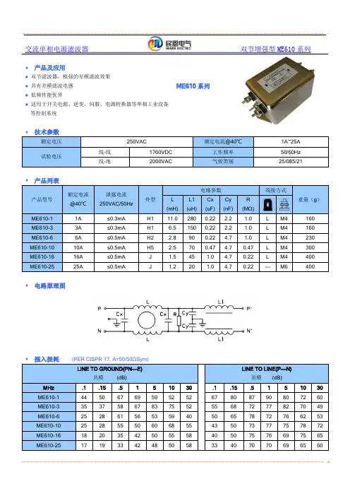
交流单相电源滤波器双节增强型ME610系列◆ 产品及应用● 双节滤波器,极强的差模滤波效果 ● 具有差模滤波电感 ● 低频性能优异● 适用于开关电源、逆变、伺服、电源转换器等单相工业设备等控制系统ME610系列◆ 技术参数额定电压 250VAC额定电流@40℃1A~25A 试验电压线-线 1760VDC 工作频率 50/60Hz 线-地2000VAC气候类别25/085/21◆ 产品列表产品型号额定电流 @40℃ 泄露电流 250VAC/50Hz 外型电路参数端接方式重量(g )L (mH)L1 (uH) Cx (uF) Cy (nF) R (MΩ)ME610-1 1A ≤0.3mA H1 11.0 280 0.22 2.2 1.0 L M4 160 ME610-3 3A ≤0.3mA H1 6.5 150 0.22 2.2 1.0 L M4 160 ME610-6 6A ≤0.5mA H2 2.8 90 0.22 4.7 1.0 L M4 230 ME610-10 10A ≤0.5mA H5 2.5 70 0.47 4.7 0.47 L M4 300 ME610-16 16A ≤0.5mA J 1.5 45 1.0 4.7 0.22 L M4 400 ME610-2525A≤0.5mAJ1.2201.04.70.22--- M6400◆ 电路原理图◆ 插入损耗 (PER CISPR 17; A=50/50ΩSym)LINE TO GROUND(PN---E)共模 (dB)LINE TO LINE(P---N)差模 (dB) MHz .1 .15 .5 1 5 10 30 .1 .15 .5 1 5 10 30 ME610-1 44 50 67 69 59 52 52 67 80 87 90 80 72 60 ME610-3 35 37 58 67 83 75 52 55 68 72 77 82 70 49 ME610-6 25 28 61 56 53 59 40 50 65 78 72 76 62 53 ME610-10 25 28 55 50 60 68 55 43 50 73 77 75 78 72 ME610-16 18 20 35 42 50 55 58 40 50 75 76 69 75 65 ME610-251719334248505833407070696560◆外形尺寸(mm)上海民恩电气有限公司。
EMI2121, SZEMI2121Single Pair Common Mode Filter with ESD Protection DescriptionThe EMI2121 is an integrated common mode filter providing both ESD protection and EMI filtering for high speed serial digital interfaces such as USB2.0.The EMI2121 provides EMI filtering for one differential data line pair and ESD protection for one data pair plus a supply input such as USB2.0 Vbus or USB ID pin. It is supplied in a small RoHS−compliant WDFN8 package.Features•Highly Integrated Common Mode Filter (CMF) with ESD Protection provides protection and EMI Reduction for systems using high speed Serial Data Lines with cost and space savings over Discrete Solutions •Large Differential Mode Bandwidth with Cutoff Frequency > 2 GHz •High Common Mode Stop Band Attenuation: >25 dB at 700 MHz, >30 dB at 800 MHz Typical•Provides ESD Protection to IEC61000−4−2 Level 4, ±12 kV Contact Discharge•Low Channel Input Capacitance provides Superior Impedance Matching Performance•Low Profile Package with Small Footprint in WDFN8 2.0 mm length x 2.2 mm width x 0.75 mm height Pb−Free Package•SZ Prefix for Automotive and Other Applications Requiring Unique Site and Control Change Requirements; AEC−Q101 Qualified and PPAP Capable•These Devices are Pb−Free, Halogen Free/BFR Free and are RoHS CompliantApplications•USB2.0 and other High Speed Differential Data Lines in Mobile Phones, Digital Still Cameras, and Automotive interfaces •MIPI D−PHYDevice Package Shipping†ORDERING INFORMATIONEMI2121MTTAG WDFN8(Pb−Free)3000/T ape & ReelWDFN8CASE 511BNMARKINGDIAGRAMSIMPLIFIED SCHEMATIC†For information on tape and reel specifications, including part orientation and tape sizes, please refer to our Tape and Reel Packaging Specification Brochure, BRD8011/D.(Note: Microdot may be in either location)PIN CONNECTIONSC2= Specific Device CodeM= Date CodeG= Pb−Free Device1Out_1+Out_1−In_1+In_1−V DD/I D GNDGNDGND(Top View)Internal(ASIC) External(Connector)SZEMI2121MTTAG WDFN8(Pb−Free)3000/T ape & ReelPIN DESCRIPTIONPin No.Pin Name Type Description1In_1+I/O CMF Channel 1+ to Connector (External)2In_1−I/O CMF Channel 1− to Connector (External)8Out_1+I/O CMF Channel 1+ to ASIC (Internal)7Out_1−I/O CMF Channel 1− to ASIC (Internal)6V DD/I D I/O Supply Protection to Connector (External)3,4,5GND GND GroundMAXIMUM RATINGS (T A = 25°C unless otherwise stated)Parameter Symbol Value Units Operating Temperature Range T OP−40 to +85°C Storage Temperature Range T STG−65 to +150°C Maximum Lead Temperature for Soldering Purposes (1/8” from Case for 10 Seconds)T L260°C DC Current per Line I LINE100mA Stresses exceeding those listed in the Maximum Ratings table may damage the device. If any of these limits are exceeded, device functionality should not be assumed, damage may occur and reliability may be affected.ELECTRICAL CHARACTERISTICS (T A = 25°C unless otherwise specified)Parameter Symbol Test Conditions Min Typ Max Unit Channel Leakage Current I LEAK T A = 25°C, V IN = 5 V, GND = 0 V 1.0m A Channel Negative Voltage V F T A = 25°C, I F= 10 mA0.1 1.5VChannel Input Capacitance to ground (Pins 1,2,4,5 to Pins 3,8)C IN T A = 25°C, At 1 MHz, GND = 0 V,V IN = 1.65 V0.8 1.3pFChannel Resistance (Pins 1−16, 2−15, 4−13,5−12, 7−10 and 9−9)Rch8.0W Differential Mode Cut*Off Frequency f3dB50 W source and load termination 2.0GHz Common Mode Stop Band Attenuation F atten@ 800 MHz30dBIn−system ESD Withstand Voltagea) Contact discharge per IEC 61000−4−2 standard, Level 4 (External Pins)b) Contact discharge per IEC 61000−4−2 standard, Level 1 (Internal Pins)V ESD(Notes 1 and 2)±12±2kVTLP Clamping Voltage (See Figure 9)V CL Forward I PP = 8 AForward I PP = 12 AReverse I PP = −8 AReverse I PP = −12 A1316−6−8.5VVVVReverse Working Voltage V RWM(Note 3) 5.0V Breakdown Voltage V BR I T = 1 mA; (Note 4) 5.59.0V Maximum Peak Pulse Current (Pin 6 to GND)I PP8x20 m s Waveform12A Clamping Voltage (Pin 6 to GND)V C I PP = 5 A10VDynamic Resistance Positive Transients Negative Transients R DYN T A= 25C, I PP=1 A, t P= 8/20 us,Any I/O to GND0.670.59WW1.Standard IEC 61000−4−2 with C Discharge = 150 pF, R Discharge = 330, GND grounded.2.These measurements performed with no external capacitor.S devices are normally selected according to the working peak reverse voltage (V RWM), which should be equal or greater than the DCor continuous peak operating voltage level.4.V BR is measured at pulse test current I T.Normal (Differential) ModeFigure 1. Normal (Differential) Mode TestConfigurationFigure 2. Application CircuitTYPICAL CHARACTERISTICSFigure 3. Differential Mode Attenuation vs.Frequency (Zdiff = 100 W)Figure 4. Common Mode Attenuation vs.Frequency (Zcomm = 50 W)Figure 5. Differential Return Loss vs. Frequency(Zdiff=100 W)Figure 6. Differential Impedance vs. Frequency(Zdiff=100 W)Figure 7. EMI2121 Measured Eye Diagram @ 480 MbpsTransmission Line Pulse (TLP) MeasurementsTransmission Line Pulse (TLP) provides current versus voltage (I −V) curves in which each data point is obtained from a 100 ns long rectangular pulse from a charged transmission line. A simplified schematic of a typical TLP system is shown in Figure 8. TLP I −V curves of ESD protection devices accurately demonstrate the product’s ESD capability because the 10 s of amps current levels and under 100 ns time scale match those of an ESD event. This is illustrated in Figure 9 where an 8 kV IEC61000−4−2 current waveform is compared with TLP current pulses at 8 and 16 A. A TLP curve shows the voltage at which the device turns on as well as how well the device clamps voltage over a range of current levels. Typical TLP I −V curves for the EMI2121 are shown in Figure 10.Figure 8. Simplified Schematic of a Typical TLP SystemFigure 9. Comparison Between 8 kV IEC61000−4−2 and 8 A and 16 A TLP WaveformsFigure 10. Positive and Negative TLP WaveformsESD Voltage ClampingFor sensitive circuit elements it is important to limit the voltage that an IC will be exposed to during an ESD event to as low a voltage as possible. The ESD clamping voltage is the voltage drop across the ESD protection diode during an ESD event per the IEC61000−4−2 waveform. Since the IEC61000−4−2 was written as a pass/fail spec for larger systems such as cell phones or laptop computers it is not clearly defined in the spec how to specify a clamping voltage at the device level. ON Semiconductor has developed a way to examine the entire voltage waveform across the ESD protection diode over the time domain of an ESD pulse in the form of an oscilloscope screenshot, which can be found on the datasheets for all ESD protection diodes. For more information on how ON Semiconductor creates these screenshots and how to interpret them please refer to On Semiconductor Application Notes AND8307/D and AND8308/D.IEC61000−4−2 Spec.Level Test Volt-age (kV)First Peak Current (A)Current at 30 ns (A)Current at 60 ns (A)127.5422415843622.51264830168IEC61000−4−2 WaveformFigure 12. 8 x 20 ms Pulse Waveform1009080706050403020100t, TIME (m s)% O F P E A K P U L S E C U R R E N TFigure 13. ESD Clamping Voltage +8 kV per IEC6100−4−2 (external to internal pin)Figure 14. ESD Clamping Voltage −8 kV per IEC6100−4−2 (external to internal pin)Micro USBConnector(Top View)Figure 15. EMI2121 Micro − USB Connector Application DiagramWDFN8, 2.2x2, 0.5PCASE 511BN ISSUE ADATE 11 DEC 2012NOTES:1.DIMENSIONING AND TOLERANCING PER ASME Y14.5M, 1994.2.CONTROLLING DIMENSION: MILLIMETERS.3.DIMENSION b APPLIES TO PLATED TERMINAL AND IS MEASURED BETWEEN 0.15 AND 0.25 mm FROM TERMINAL.4.COPLANARITY APPLIES TO THE EXPOSED PAD AS WELL AS THE TERMINALS.BOTTOM VIEW2XSEATING PLANEDIM MIN MAX MILLIMETERS A 0.700.80A10.000.05b 0.150.25D 2.20 BSC D20.340.54E 2.00 BSC E20.600.80e 0.50 BSC L10.050.15L20.300.50L30.150.25DIMENSIONS: MILLIMETERS*For additional information on our Pb −Free strategy and soldering details, please download the ON Semiconductor Soldering and Mounting Techniques Reference Manual, SOLDERRM/D.RECOMMENDEDGENERICMARKING DIAGRAM*XX = Specific Device Code M = Date Code G = Pb −Free Device*This information is generic. Please referto device data sheet for actual part marking.Pb −Free indicator, “G” or microdot “ G ”,may or may not be present.L1DETAIL AOPTIONAL CONSTRUCTIONSDETAIL BOPTIONAL CONSTRUCTIONSA30.20 REF b10.250.35L 0.750.95DETAIL Cb1SOLDERING FOOTPRINT*MECHANICAL CASE OUTLINEPACKAGE DIMENSIONSON Semiconductor and are trademarks of Semiconductor Components Industries, LLC dba ON Semiconductor or its subsidiaries in the United States and/or other countries.ON Semiconductor reserves the right to make changes without further notice to any products herein. ON Semiconductor makes no warranty, representation or guarantee regarding the suitability of its products for any particular purpose, nor does ON Semiconductor assume any liability arising out of the application or use of any product or circuit, and specifically disclaims any and all liability, including without limitation special, consequential or incidental damages. ON Semiconductor does not convey any license under its patent rights nor thePUBLICATION ORDERING INFORMATIONTECHNICAL SUPPORTNorth American Technical Support:Voice Mail: 1 800−282−9855 Toll Free USA/Canada Phone: 011 421 33 790 2910LITERATURE FULFILLMENT :Email Requests to:*******************onsemi Website: Europe, Middle East and Africa Technical Support:Phone: 00421 33 790 2910For additional information, please contact your local Sales Representative。
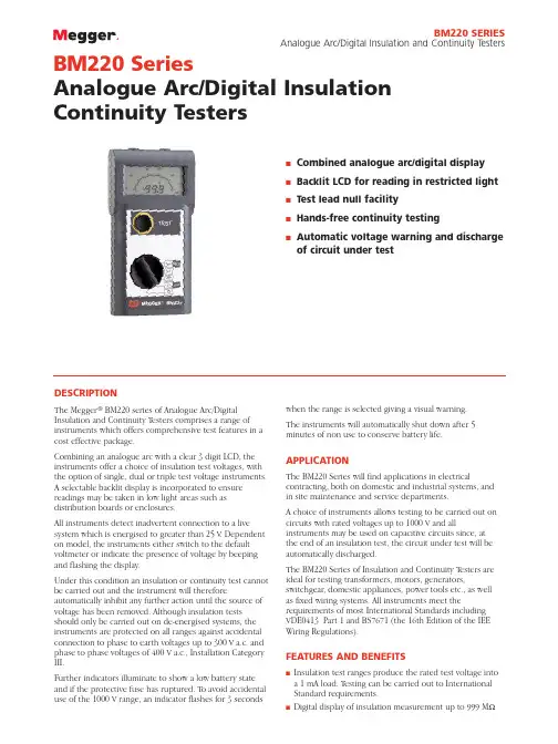
BM220 SeriesAnalogue Arc/Digital Insulation Continuity Testers DESCRIPTIONThe Megger®BM220 series of Analogue Arc/Digital Insulation and Continuity T esters comprises a range of instruments which offers comprehensive test features in a cost effective package.Combining an analogue arc with a clear 3 digit LCD, the instruments offer a choice of insulation test voltages, with the option of single, dual or triple test voltage instruments.A selectable backlit display is incorporated to ensure readings may be taken in low light areas such as distribution boards or enclosures.All instruments detect inadvertent connection to a live system which is energised to greater than 25 V. Dependent on model, the instruments either switch to the default voltmeter or indicate the presence of voltage by beeping and flashing the display.Under this condition an insulation or continuity test cannot be carried out and the instrument will therefore automatically inhibit any further action until the source of voltage has been removed. Although insulation tests should only be carried out on de-energised systems, the instruments are protected on all ranges against accidental connection to phase to earth voltages up to 300 V a.c. and phase to phase voltages of 400 V a.c., Installation Category III.Further indicators illuminate to show a low battery state and if the protective fuse has ruptured. T o avoid accidental use of the 1000 V range, an indicator flashes for 3 seconds when the range is selected giving a visual warning.The instruments will automatically shut down after 5 minutes of non use to conserve battery life. APPLICATIONThe BM220 Series will find applications in electrical contracting, both on domestic and industrial systems, andin site maintenance and service departments.A choice of instruments allows testing to be carried out on circuits with rated voltages up to 1000 V and all instruments may be used on capacitive circuits since, atthe end of an insulation test, the circuit under test will be automatically discharged.The BM220 Series of Insulation and Continuity T esters are ideal for testing transformers, motors, generators, switchgear, domestic appliances, power tools etc., as wellas fixed wiring systems. All instruments meet the requirements of most International Standards including VDE0413 Part 1 and BS7671 (the 16th Edition of the IEE Wiring Regulations).FEATURES AND BENEFITSs Insulation test ranges produce the rated test voltage into a 1 mA load. T esting can be carried out to International Standard requirements.s Digital display of insulation measurement up to 999 MΩs Combined analogue arc/digital displays Backlit LCD for reading in restricted light s Test lead null facilitys Hands-free continuity testings Automatic voltage warning and discharge of circuit under testBM220 SERIESAnalogue Arc/Digital Insulation and Continuity TestersBM220 SERIES Analogue Arc/Digital Insulation and Continuity TestersBM220 SERIES Analogue Arc/Digital Insulation and Continuity TestersUKArchcliffe Road Dover CT17 9EN EnglandT +44 (0) 1304 502101 F +44 (0) 1304 207342UNITED STATES4271 Bronze WayDallas TX 75237-1088 USAT 800 723 2861 (USA only)T +1 214 333 3201F +1 214 331 7399OTHER TECHNICAL SALES OFFICESValley Forge USA, Toronto CANADA,Mumbai INDIA, Trappes FRANCE,Sydney AUSTRALIA, Madrid SPAINand the Kingdom of BAHRAIN.Registered to ISO 9001:2000 Reg no. Q 09290Registered to ISO 14001 Reg no. EMS 61597BM220_DS_en_V10The word ‘Megger’ is a registeredtrademark。
MIC4834Low Noise Dual 220 V PP EL DriverMLF and Micro Lead Frame are registered trademark of Amkor TechnologiesMicrel Inc. • 2180 Fortune Drive • San Jose, CA 95131 • USA • tel +1 (408) 944-0800 • fax + 1 (408) 474-1000 • General DescriptionThe MIC4834 is a low noise dual Electroluminescent (EL) Panel driver used in backlighting applications. The MIC4834 converts a low DC voltage to a high DC voltage using a boost converter and then alternates the high DC voltage across the EL panels using an H-bridge. The MIC4834 incorporates internal wave-shaping circuitry specifically designed to reduce audible noise emitted by EL panels. With only one inductor the MIC4834 can drive two outputs and requires a minimum number of passive components. It features an operating input voltage range of 2.3V to 5.8V, making it suitable for 1-cell Li-ion and 2- or 3-cell alkaline/NiCad/NiMH battery applications.The MIC4834 features separate oscillators for the boost and H-bridge stages. The boost frequency may be adjusted with an external resistor to optimize efficiency and brightness. The H-bridge frequency is internally preset to 225Hz, to reduce the number of external components and layout space.The MIC4834 is available in 10 pin 3mmx3mm MLF ® package as well as MSOP-10L, and has an operating junction temperature range of –40°C to +125°C.Features•Drives two EL panels, up to 3 in 2 each at full brightness• 220V PP regulated AC output waveform • 2.3V to 5.8V DC input voltage• Wave-shaping circuit to reduce audible noise • Adjustable boost converter frequency • Single inductor to power both panels • 0.1µA typical shutdown current • Package options− 10-pin 3mmx3mm MLF ® − 10-pin MSOP• –40oC to +125o C junction temperature rangeApplications• Mobile phones• MP3/portable media players (PMP) • Clocks/ watches • Remote controls • Cordless phones • GPS devices • PDAs_________________________________________________________________________________________________Typical ApplicationLow Noise Dual EL DriverOrdering InformationPart Number Package Operating Junction Temp RangeLead Finish MIC4834YML10 pin (3mm x 3mm) MLF®-40ºC to +125ºC Pb-free / RoHS-CompliantMIC4834YMM 10-Pin MSOP -40ºC to +125ºC Pb-free / RoHS-Compliant Pin Configuration10-Pin MLF® - Top View 10-Pin MSOP – Top ViewPin DescriptionPin Number Pin Name Pin Function1 ENA EL Panel A Enable Pin: Logic high enables ELA and logic low disables ELA output.2 VDD DC Input Supply Voltage: 2.3V to 5.8V3 RSWRSW pin: Sets internal boost converter switch frequency by connecting an externalresistor (R SW) to VDD. Connecting the R SW resistor to GND shuts down the device.4 ENB EL Panel B enable pin: Logic high enables ELB and logic low disables ELB output.5 GNDGround.6 SW Switch Node: Drain of internal high-voltage power MOSFET for boost circuit.7 CSRegulated Boost Output: Connect to the output capacitor of the boost regulator andto the cathode of the diode.8 COMEL output: Common EL output terminal to both ELA and ELB. Connect one end ofeach EL panel to this pin.9 ELB EL Panel B output: Connect the other end of the EL panel B to this pin.10 ELA EL Panel A output: Connect the other end of the EL panel A to this pin.EPad HS Pad Heat Sink Pad. Connect to ground externally. MLF® package only.Absolute Maximum Rating(1)Supply voltage (V DD).......................................-0.5V to 6.5V Output voltage (V CS)...................................... -0.5V to 130V Switch Node (V SW).........................................-0.5V to 130V Enable Voltage (V RSW, V ENA, V ENB)...................-0.5V to 6.5V Ambient Storage Temperature (T S) ...........-65ºC to +150ºC ESD Rating(3)...........................................................................ESD Sensitive Operating Range(2)Supply Voltage (V DD)........................................2.3V to 5.8V Switching MOSFET Frequency (f SW)........35kHz to 350kHz Enable Voltage (V RSW, V ENA,,V ENB).......................0V to V DD Junction Temperature Range (T J).............-40°C to +125°C Package Thermal Impedance3mm x 3mm MLF® (θJA)……………………........60°C/W MSOP(θJA)…………………….........................206°C/WElectrical Characteristics(4)T A = 25o C, V DD= 3.0V unless otherwise noted. Bold values indicate -40°C ≤ T J≤ 85°C.Symbol Parameter Condition Min Typ Max UnitsV DD Supply Voltage Range 2.3 5.8 VI DD InputSupplyCurrent V RSW = High; V CS = 105V;ELA, ELB, COM = Open152 220 µAI SD ShutdownCurrent V RSW = Low; V DD = 5.8V 0.1 1 µAR DS(ON) On-resistance Of Switching Transistor I SW = 100mA, V CS = 105V 6.0 12.0 ΩV CS Output voltage Regulation V DD = 2.3V to 5.8v 90 109 120 VV DD = 3.0V(R SW = 1.3MΩ )25 35 45 kHzV DD = 3.0V (R SW = 450kΩ) 75 100 125 kHzf Sw Boost Switching FrequencyV DD = 3.0V(R SW = 125kΩ)250 350 450 kHzf EL ELA, ELB and COM Drive Frequency V DD = 3.0VELA, ELB, COM = Open165 225 285 HzD Switching Transistor Duty Cycle 80 95 %I OUT Output Current Drive Limit 2.5 5 7.5 mAV ENA,V ENBEnable Logic Threshold 0.4 1.2 VV HYS Enable Logic Hysteresis 20 50 150 mVI ENA,I ENBEnable Input Current 0.1 1 µA Notes:1. Exceeding the absolute maximum rating may damage the device.2. The device is not guaranteed to function outside its operating rating.3. Devices are ESD sensitive. Handling precautions recommended. Human body model, 1.5kΩ in series with 100pF.4. Specification for packaged product only.Typical CharacteristicsFunctional DiagramFigure 1. MIC4834 Block Diagram Functional DescriptionOverviewThe MIC4834 is a high-voltage dual output EL driver with a peak-to-peak AC output voltage of 220V capable of driving two 3 in2 EL panels. The MIC4834 drives EL panels by converting a low DC input voltage to a high DC high output voltage using the boost regulator circuit and then alternating the high DC voltage across the EL panel using an H-Bridge. Input supply current for the MIC4834 is typically 152µA. The high voltage EL driver has two internal oscillators to control the boost switching frequency and the H-bridge driver frequency. The internal boost oscillator frequency can be individually programmed through an external resistor to maximize efficiency and brightness of the EL panel. The H-bridge frequency is internally fixed at 225Hz to reduce external component count.R egulationReferring to Figure 1, power is initially applied to V DD. When the internal feedback voltage is less than the reference voltage, the internal comparator enables switching in the boost circuit. When the boost regulator is switching, current flows through the inductor into the switch. The switching MOSFET will typically turn on for 90% of the switching period. During the on-time, energyis stored in the inductor. When the switching MOSFET turns off, current flowing into the inductor forces the voltage across the inductor to reverse polarity. The voltage across the inductor rises until the external diode conducts and clamps the voltage at V OUT + V D1. The energy in the inductor is then discharged into the C OUT capacitor. The internal comparator continues to turn the switching MOSFET on and off until the internal feedback voltage is above the reference voltage. Once the internal feedback voltage is above the reference voltage, the internal comparator disables switching. The control circuit will continue to turn the MOSFET’s on and off to maintain a constant DC voltage at the CS pin.When the MIC4834 EL Driver is enabled, ELA and ELB will switch in opposite states with COM to achieve a 220V peak-to-peak AC output signal needed to drive the two EL panels.Switching FrequencyThe switching frequency of the converter is controlled by an external resistor (R SW ) between RSW and VDD. The switching frequency increases as the resistor value decreases. In general, the lower the switching frequency, the greater the input current is drawn to deliver more power to the output. Lowering the switching frequency can be used to drive larger panels. However, the switching frequency should not be so low as to allow the voltage at the switch node or the CS pin to exceed the absolute maximum voltage of those pins. For resistor value selections, see the “Typical Characteristics: Switching Frequency vs. SW Resistor” graph on Page 4 or use the equation below. The switching frequency range is 35kHz to 350kHz, with an accuracy of ±20%.()Ω=M R 46(kHz)f SW SWEL FrequencyThe MIC4834 EL panel frequency is internally fixed at 225Hz.Enable FunctionThere are a few different ways to enable and disable the MIC4834. The boost regulator may be disabled by pulling the R SW resistor to ground. This turns off both the EL panels by cutting power to the device completely. The R SW resistor must be pulled to VDD to enable the boost oscillator. If it is not equal to VDD, then the frequency set by R SW will be different the programmed value.For individual panel control, the ENA and ENB pins can be used to enable ELA and ELB, respectively. Pulling ENA or ENB high (over 1.2V) or low (below 0.4V) willturn ELA and ELB panels on or off.Figure 2. EL Panel Waveform – 2 × 1 in2Figure 3. EL Panel Waveform – 2 × 2 in 2Figure 4. EL Panel Waveform – 2 × 3 in 2Application InformationThe MIC4834 is designed to use an inductance with a value between 100µH to 330µH. Choosing the right inductor is always a balance of size, inductance, efficiency, current rating and cost. A TDK (VLS4012T-221M) 220µH inductor is recommended based on size, efficiency and current rating.Generally, the lower the inductance, the more current the inductor can handle. Lowering the inductance allows the boost regulator to draw more input current to deliver more energy every switching cycle. As a result, a lower inductance may be used to drive larger panels or brighten similar sized panels. However, caution is required as using a low inductance with a low switching frequency may cause the voltage at the switch node and the CS pin to exceed the absolute maximum rating. If the application uses a low input voltage (2.3V to 3V), then a lower value inductor, such as 100µH, may be used in order to drive the EL panel at maximum brightness.DiodeThe diode must have a high reverse voltage (150V), since the output voltage at the CS pin can reach up to 130V. A fast switching diode with lower forward voltage and higher reverse voltage (150V), such as BAV20WS/BAS20W, can be used to enhance efficiency. Output CapacitorLow ESR capacitors should be used at the regulated boost output (CS pin), to minimize the switching output ripple voltage. The larger the output capacitance, the lower the output ripple at the CS pin. The reduced output ripple, at the CS pin, along with a low ESR capacitor improves the efficiency of the MIC4834 circuit. Selection of the capacitor value depends upon the peak inductor current, inductor size, and the load. The MIC4834 is designed for use with an output capacitance as low as 2.2nF. For minimum audible noise, the use of a C0G/NPO dielectric output capacitor is recommended. TDK and AVX offer C0G/NPO dielectric capacitors in capacitance up to 2.7nF at 200V to 250V voltage rating in 0805 size.EL Panel Terminals (ELA, ELB, COM)The two EL panels are connected from ELA to COM and ELB to COM. The ELA and ELB terminals are in phase with each other, while the COM is out of phase with both ELA and ELB. Since ELA and COM are out of phase, the high voltage generated by the boost regulator is alternated across ELA and COM by the H-Bridge. The frequency of each cycle is internally fixed at 225Hz. The alternating 220V peak-to-peak causes the EL panel to emit light. Similarly, the ELB and COM are also out of phase and allows a second EL panel to be driven at the same time. Both EL panels may operate independently from each other and do not have to be the same size. For component selection, Table 2 lists recommended values for various panel sizes up to a total of 6 in2 (For example, two 3 in2 panels). Driving overly large panels will result in a dimmer display, but will not cause damage to the device.Application CircuitFigure 6. Typical Li-Ion Powered MIC4834 CircuitNote: Table 2 applies to circuit shown in Figure 6.Total Panel Area (in 2) 0.4 1 2 3 4 5 6 Capacitance (nF)251015202530R SW (k Ω) 357 392 487 562 750 931 1100 f SW (kHz)128 116 94 82 62 50 42Table 2. Recommended R SW Values for Total Panel SizesBill of MaterialsItem Part NumberManufacturerDescriptionQty C1 C1608X7R1A103K TDK (1) 0.01µF Ceramic Capacitor, 10V, X7R, Size 0603 1 C2 C1608X5R0J106K TDK (1) 10 µF Ceramic Capacitor, 6.3V, X5R, Size 0603 1 C3 C2012C0G2E2222J TDK (1)0.0022µF Ceramic Capacitor, 250V, C0G, Size 0805 1 L1 VLS4012T-221M TDK (1) 220µH, 210mA I SAT . (4mmx4mmx1.2mm) 1 D1 BAS20-V-GS18 Vishay (2) 200V/200mA Hi-Voltage Switching Diode1 R1 or R SW CRCW06033323FKEYE3 Vishay (2) 332k Ω, 1%, 1/16W, Size 06031 U1 MIC4834YMLMicrel (3)Low Noise Dual 220Vp-p EL Driver with Output Slew Control1Notes:1. TDK: 2. Vishay: 3.Micrel, Inc .: Layout Recommendation (MLF®)Top LayerBottom LayerLayout Recommendation (MSOP)Top LayerBottom LayerPackage Information10-Pin 3mm x 3mm MLF® (ML)10-Pin MSOP (MM)。
EMI滤波器适用范围与应用要求选择该类合适的型号与参数的EMI滤波器可用于吸收古瑞瓦特生产的小功率光伏逆变器的交流输出回路产生的浪涌与尖峰谐波电压标准的EMI滤波器通常由串联电抗器和并联电容器组成的低通滤波电路,其作用是允许设备正常工作时的频率信号进入设备,而对高频的干扰信号有较大的阻碍作用。
一、基本信息模块中文名称:EMI滤波器输出阻抗:50(kΩ)输入阻抗:40(kΩ)总频差:343(MHz)二、序言:电源线是干扰传入设备和传出设备的主要途径,通过电源线,电网的干扰可以传入设备,干扰设备的正常工作,同样设备产生的干扰也可能通过电源线传到电网上,干扰其他设备的正常工作。
因此:必须在设备的电源进线处加入EMI滤波器。
三、EMI滤波器的基本技术参数:输出阻抗:50(kΩ)输入阻抗:40(kΩ)阻带衰减:30(dB)插入损耗:50(dB)基准温度:70(℃)激励电平:50(mW)负载谐振电阻:430(Ω)负载电容:53.5(pF)总频差:343(MHz)温度频差:54(MHz)调整频差:554(MHz)标称频率:50(MHz)工作频率:工频50/60Hz或者中频400Hz种类:滤波器型号:SH-100四、典型结构1、低通滤波器:EMI滤波器是一种由电感和电容组成的低通滤波器,它能让低频的有用信号顺利通过,而对高频干扰有抑制作用。
EMI滤波器的典型结构如图所示。
EMI滤波器的作用,主要体现在以下两个方面:1.1、抑制高频干扰抑制交流电网中的高频干扰对设备的影响;1.2、抑制设备干扰抑制设备(尤其是高频开关电源)对交流电网的干扰。
2、性能指标任何一种产品都有它特定的性能指标,或者是客户所期望的,或者是某些标准所规定的。
EMI滤波器最重要的技术指标是对干扰的抑制能力,常常用所谓的插入损耗(Insertion Loss)来表示。
它的定义是:没有接入滤波器时从干扰源传输到负载的功率P1和接入滤波器后从干扰源传输到负载的功率P2之比,用分贝(dB)表示。