256抽头精密数字电位器AD5160测试程序
- 格式:docx
- 大小:13.55 KB
- 文档页数:2
第一章系统安装和启动一实验系统工作方式爱迪克T598实验系统可以工作在三种方式下,下面进行详细介绍。
1.爱迪克T598实验系统工作在51串口实验/仿真方式(1)用户根据实验要求,进行MCS-51单片机实验/仿真时(8032芯片已插在D33插座上),将XC9(CPU插座)与XC1(CPU51插座)用T598A-C连接板连接起来,XC6(CPU88插座)空。
(2)用实验机配套的串行通讯电缆,将9芯电缆的一端与实验机上的9芯插座相连,另一端与PC机的串行口相连。
(3)打开电源,在PC机上打开LCA51软件,运行实验程序,具体操作参见《爱迪克T598_51使用说明》。
2.爱迪克T598实验系统工作在88串口实验方式(1)用户根据实验要求,进行MCS-88单片机实验时,将XC9(CPU插座)与XC6(CPU88插座)用T598A-C连接板连接起来,XC1(CPU51插座)空。
(2)用实验机配套的串行通讯电缆,将9芯电缆的一端与实验机上的9芯插座相连,另一端与PC机的串行口相连。
(3)打开电源,在PC机上打开LCA88ET软件,运行实验程序,具体操作参见《T598_88使用说明》。
3.爱迪克T598实验系统工作在96串口实验/仿真方式(1)进行MCS-96单片机实验时,将T598A-96板插入XC9(CPU插座)和XC5(CPU96插座),XC6(CPU88插座)和XC1(CPU51插座)空。
(2)用实验机配套的串行通讯电缆,将9芯电缆的一端与实验机上的9芯插座相连,另一端与PC机的串行口相连。
(3)打开电源,运行仿真调试软件LCA96ET,具体操作参见《爱迪克T598_96使用说明》。
二AEDK598实验系统工作在MCS51方式下开关初始状态●XB、XB1 : 短路套全插上。
●XB2,XB5 : 短路套向上插(SPEAK端),第10模块处于放音功能。
●第○4模块中:多位开关K3拨向最左(温度控制)端,做温度控制实验用。
德信诚培训网平板电脑轻触开关检验标准1. 目的制定本公司的检验标准和试验方法,确保本公司所有轻触开关能满足研发设计、生产装配以及用户的使用要求。
2. 适用范围本规程适用于本公司所有轻触开关材料的检验。
3.抽样标准依据GB/T2828.1-2003正常检验一次抽样方案II级水平,其它根据抽样标准书执行。
严重缺陷(CR)AQL=0;主要缺陷(Maj)AQL=0.65;次要缺陷(Min)AQL=1.5。
3.1致命缺陷:(Critical)危及人生安全,易招致不安全因素的项目以及导致其基本功能失效的项目。
3.2严重缺陷:(Major)不会危及人生安全,但可能导致功能失误或降低原有使用功能的项目。
3.3次要缺陷:(Minor)单位产品的一般性质量特征不符合规定或单位产品的质量特性轻微不符合规定,对产品的使用性能没有影响或只有轻微影响的项目。
4.检验/测试环境:室内温度:25±10℃;相对湿度:60%(+15%,-10%)德信诚培训网距离:人眼与产品表面的距离为300—350mm。
或灯光垂直产品距离1米,使用40W日光灯时间:检测量面和其它不超过8s;每件检查总时间不超过30s(除首件)。
光照亮度:300~700Lux;目视条件:正常视力,1.0以上;(每个表面来回观看5秒)目视位置:产品放置检验者正前面的30cm距离处,检验者于产品成水平垂直±30°5.检验内容及标准在轻触开关手柄的顶端面中央,按轻触开关动作方向均匀地施将试样引脚浸过助焊剂后,沿轴线方向浸入265±5℃的Sn96.5 物料)、260±5℃的Sn63pb37(非RoHS 物5±0.5s ,本体距熔融焊料1.5mm 。
开关应 B在三个互相垂直的轴线方向上依次振,加速度为50.0m/s2,振动时间55min.开关应无破裂、变形、位移或零件松动;开关的功能动作、接6.参考文件制定本规范参考了下列文件中的一些信息,但没有直接引用里面的条文。
ap5160 电流计算方法Ap5160 is a popular current measurement tool used in various industries to accurately measure and monitor current flow. It is essential to understand the calculation methods involved in using ap5160 to ensure accurate readings and reliable data. By using the appropriate formulas and techniques, users can obtain precise current measurements for their specific applications.对于许多行业来说,ap5160是一种常用的电流测量工具,能够准确地测量和监测电流流动。
了解使用ap5160所涉及的计算方法是至关重要的,以确保准确的读数和可靠的数据。
通过使用适当的公式和技术,用户可以获取他们特定应用中的精确电流测量。
One of the key calculation methods used with ap5160 is Ohm's Law, which states that the current flowing through a conductor is directly proportional to the voltage across the conductor and inversely proportional to the resistance of the conductor. By applying this fundamental principle, users can calculate the current flowing through a circuit with precision and accuracy. Ohm's Law provides asimple yet powerful formula for determining current in a circuit, making it an essential tool for users of ap5160.与ap5160一起使用的关键计算方法之一是欧姆定律,该定律规定通过导体的电流与导体两端的电压成正比,与导体的电阻成反比。
51单片机板子功能测试
1.芯片检测:通过读取板子上的芯片信息,确认是否使用了正确的
51单片机芯片,以及芯片的版本信息。
2.闪存测试:通过在闪存中写入测试代码,然后执行代码,验证闪存
的可读写性以及执行功能正常。
3.存储器测试:包括片内RAM和片外扩展存储器的测试,通过写入和
读取随机数据,并进行校验,验证存储器的可靠性。
4.输入输出测试:测试板子上的各种输入输出接口是否能正常工作,
包括数字输入输出口、模拟输入输出口、通信接口(如串口、I2C、SPI
等)等。
5.定时器测试:通过配置定时器,产生不同频率和占空比的脉冲信号,来测试定时器的准确性和稳定性。
6.PWM测试:通过配置PWM输出,测量占空比和频率,并验证输出的
正常性。
7.中断测试:通过外部中断引脚或定时器中断,测试中断的触发和处
理功能是否正常。
8.ADC/DAC测试:测试模拟输入输出的精度和准确性,通过模拟信号
输入和输出,验证ADC和DAC的功能。
9.LCD测试:测试板子上的LCD接口是否能正常显示字符或图形,并
验证显示的准确性。
10.通信测试:测试板子上的通信接口(如串口、I2C、SPI)是否能
与其他设备进行正常通信,并检查通信的准确性和稳定性。
通过以上这些功能测试,可以全面验证51单片机板子的各项功能是否正常,确保板子的质量和可靠性。
同时可以帮助开发人员在开发过程中排查和解决各种问题,提高开发效率。
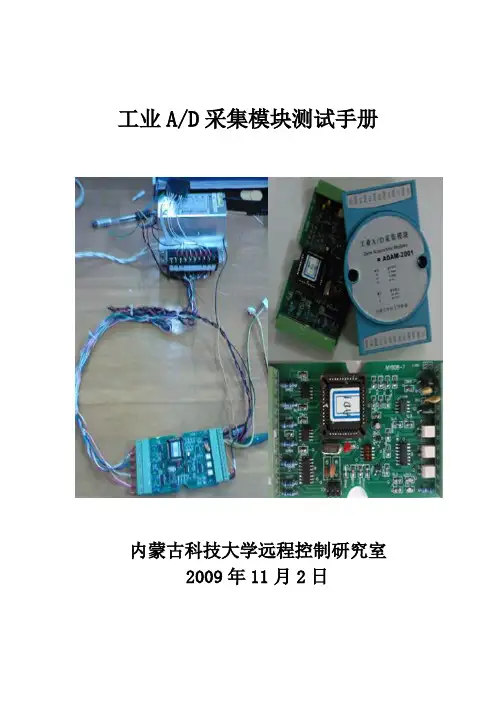
工业A/D采集模块测试手册内蒙古科技大学远程控制研究室 2009年11月2日前言由内蒙古科技大学远程控制研究室自行设计的工业A/D采集模块是一款集工业采集和现场通信为一体的电子应用模块。
它的主要功能是能够采集8路模拟信号,经过A/D转换后将转换结果存储在CPU中,并可以通过485总线将转换结果发送到其他模块。
本模块已经在热网远程监控系统中得到应用,运行稳定。
《A/D采集模块测试手册》主要是针对工业A/D采集模块在应用中出现的一些故障,比如不能正常采集数据、采集到得数据显示全部为0、采集数据显示全部满量程、采集数据值与实际值相比误差较大等等。
本手册将对以上各个故障逐一分析,并介绍如何检测各种故障产生的原因。
同时将根据产生故障的原因和实际中的一些维修经验,介绍各种故障的维修方法。
由于本手册主要是针对已经出现的一些故障进行介绍,原因分析、检测方法和维修方法大部分也是本人根据对A/D采集模块原理的了解和在实际操作中的一些经验得出的,所以手册中难免有一些错误和不足,恳请大家提出宝贵意见,以便进一步改进。
吴战国 2009年11月2日A/D模块检测方法一检测设备示波器 +5V直流电源 8个可调电位器万用表二检测环境将8个电位器(模拟8路传感器)按顺序分别接在11,12……214(8个传感器信号出入)端子上,电路原理图如图0。
图0. 电位器接线电路原理图调节8个电位器,使其电位值固定,并且8个值按照一定规律排列,用示波器观察其波形应为图 1所示。
图1. 8个电位器输出信号三检测步骤1、在接通一块A/D板后,首先测试供电电压。
a、测试结果:1)测值为+5V——正常,进行步骤2;2)测值不是+5V——检查供电电源和电源线路;b、原因分析:A/D板采用+5V的直流电供电,电压太大会损坏板上器件;电压太低会导致测出的值有大的误差。
c、可能造成的错误现象:电压太低,显示值偏低;电压太高,烧坏MAX4558,使显示值全部错误或者其中几路值太高。
电位器检验作业指导一、背景介绍电位器是一种用于调节电流或电压的电子元件,广泛应用于各种电子设备中。
为了确保电位器的质量和性能符合要求,需要进行检验作业。
本文将详细介绍电位器检验作业的步骤和标准。
二、检验设备和工具1. 万用表:用于测量电位器的电阻值、电容值等参数。
2. 直流电源:用于给电位器提供电压。
3. 示波器:用于观察电位器的电压波形。
4. 温湿度计:用于测量环境温度和湿度。
三、检验步骤1. 外观检查:检查电位器外观是否完好,无损坏、变形或腐蚀等情况。
2. 尺寸测量:使用卡尺等工具测量电位器的尺寸,确保符合设计要求。
3. 电阻测量:使用万用表测量电位器的电阻值。
将万用表的测量引线分别接到电位器的两个端子上,记录测量结果,并与设计要求进行比较。
4. 线性度测试:将电位器接入电路中,通过改变电位器的旋转角度,测量电位器输出的电压值。
记录不同角度下的电压值,并绘制线性度曲线。
线性度应在一定范围内。
5. 温度特性测试:将电位器暴露在不同温度环境下,测量电位器的电阻值。
根据测量结果绘制温度特性曲线,确保电位器在不同温度下的电阻变化在允许范围内。
6. 湿度特性测试:将电位器暴露在不同湿度环境下,测量电位器的电阻值。
根据测量结果绘制湿度特性曲线,确保电位器在不同湿度下的电阻变化在允许范围内。
7. 耐久性测试:通过旋转电位器或进行长时间使用,检验电位器的耐久性能。
观察电位器是否出现卡滞、松动、接触不良等问题。
8. 绝缘电阻测试:使用万用表测量电位器的绝缘电阻,确保绝缘电阻值符合要求。
四、检验标准1. 外观检查:电位器外观应无明显损坏、变形或腐蚀等情况。
2. 尺寸测量:电位器尺寸应符合设计要求。
3. 电阻测量:电位器的电阻值应与设计要求相符,允许一定的误差范围。
4. 线性度测试:电位器的线性度应在一定范围内,具体范围根据设计要求确定。
5. 温度特性测试:电位器的温度特性曲线应在允许范围内,具体范围根据设计要求确定。
i2c总线即twi总线调试数字电位器AD5161#include#include#define uchar unsigned char#define uint unsigned int#include "Skey.c"#define START 0X08#define MT_SLA_ACK 0X18#define MT_DATA_ACK 0X28#define Start() (TWCR=(1<<TWINT)|(1<<TWSTA)|(1<<TWEN)) //产生START信号#define Stop() (TWCR=(1<<TWINT)|(1<<TWSTO)|(1<<TWEN)) //产生STOP信号#define Wait() while(!(TWCR&(1<<TWINT))) //等待当前操作完成#define TestACK() (TWSR&0xF8) //取出状态码#define SetACK() (TWCR|=(1<<TWEA)) //产生ACK#define Writebyte(twi_d) {TWDR=(twi_d);TWCR=(1<<TWINT)|(1<<TWEN);} //发送一个字节(twi_d为写入的数据)void twi_init(){TWBR=0X20;TWSR=0;TWCR=0X44;}uchar AD5161_writeB(uchar devadd,uchar cmd,uchar rdata)//地址指令数据{Start();Wait();if(TestACK()!=START){return 0;}Writebyte(devadd);Wait();if(TestACK()!=MT_SLA_ACK){return 0;}Writebyte(cmd);Wait();if(TestACK()!=MT_DATA_ACK){return 0;}Writebyte(rdata);Wait();if(TestACK()!=MT_DATA_ACK){return 0;}Stop();delay(10);return 1;}void main(){uchar i,data=0;twi_init();AD5161_writeB(0X58,0,data); while(1){if(key_press()){i=key_scan();switch(i){case 0:data=data-16;//阻值增大break;case 1:data=data+16;//阻值减小break;case 2: //最大data=0;break;case 3:data=255; //最小break;}AD5161_writeB(0x58,0,data); }}}。
DX516大虾51仿真器用户可以同时研究光盘上的“一步步教您如何第一次使用dx516仿真器”以便更好的理解使用方法。
1。
安装将仿真器组装好,串口线按照正确方向插入仿真器,另一端和电脑串口连接,请尽量使用计算机的硬串口。
仿真器底座左边的跳线,请放在EMB这边,以进入仿真状态。
如果放在RUN这边,将会进入脱机运行状态。
晶振选择跳线请放在IN这边,以使用仿真器内部晶振,内部晶振更加可靠。
如果放在OUT这边,则会使用外部的用户板晶振。
2。
电源如果用户板使用电流不大,则可以使用usb取电,将usb取电板插入电脑的usb口中。
如果用户板使用电流比较大,估计大于100毫安以上,则请使用外置5V电源。
请拔出usb取电板,并把它从连线上取下。
3。
启动在仿真器上电,或者按一下仿真器上面的按钮时,仿真器会发出“嘀-”,表示仿真器正常启动。
同时仿真器上面的灯闪烁一次,表示正常进入仿真状态。
4。
仿真设置第一个设置:C51用户请在您的代码的main()函数前面,加上一句:char code dx516[3] _at_ 0x003b;ASM汇编用户请将你的主程序跳过中断区直到0040H以后,如:org 0000Hljmp mainorg 0040Hmain:....;程序开始如果以上设置你没有做,在装载过程中,仿真器会发出“嘀嘀嘀” 的三声短声报警,这时的仿真结果将可能不正确。
第二个设置:请在硬件仿真设置选项中,选择serial interrupt,在前面打勾。
如果以上设置你没有做,在装载过程中,仿真器会发出“嘀-” 的一声长声报警,这时的仿真结果将可能不正确。
其余设置:请选择use keil Monitor-51 Driver ,这样才会使用硬件仿真请选择load Application at start ,在启动时直接装载程序请选择Go till main ,装载后直接运行到main函数请在硬件仿真设置选项中,选择115200bps波特率,所有cache都可以不选,或者只选cache code。
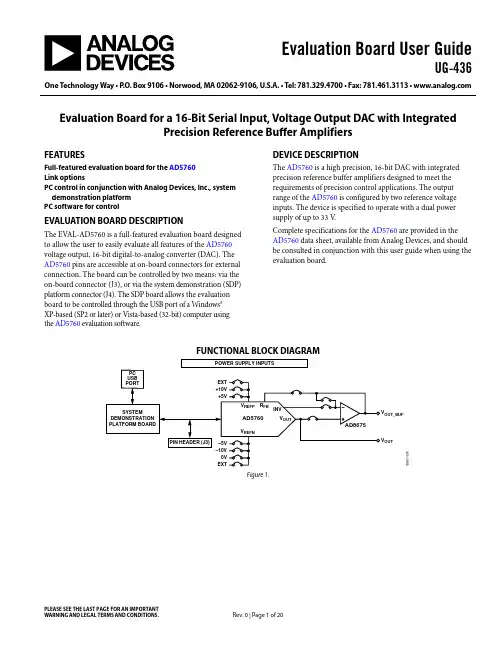
Evaluation Board User GuideUG-436One Technology Way • P .O. Box 9106 • Norwood, MA 02062-9106, U.S.A. • Tel: 781.329.4700 • Fax: 781.461.3113 • Evaluation Board for a 16-Bit Serial Input, Voltage Output DAC with IntegratedPrecision Reference Buffer AmplifiersPLEASE SEE THE LAST PAGE FOR AN IMPORTANT WARNING AND LEGAL TERMS AND CONDITIONS.Rev. 0 | Page 1 of 20FEATURESFull-featured evaluation board for the AD5760 Link optionsPC control in conjunction with Analog Devices, Inc., system demonstration platform PC software for controlEVALUATION BOARD DESCRIPTIONThe EV AL-AD5760 is a full-featured evaluation board designed to allow the user to easily evaluate all features of the AD5760 voltage output, 16-bit digital-to-analog converter (DAC). The AD5760 pins are accessible at on-board connectors for external connection. The board can be controlled by two means: via the on-board connector (J3), or via the system demonstration (SDP) platform connector (J4). The SDP board allows the evaluation board to be controlled through the USB port of a Windows® XP-based (SP2 or later) or Vista-based (32-bit) computer using the AD5760 evaluation software. DEVICE DESCRIPTIONThe AD5760 is a high precision, 16-bit DAC with integrated precision reference buffer amplifiers designed to meet the requirements of precision control applications. The output range of the AD5760 is configured by two reference voltage inputs. The device is specified to operate with a dual power supply of up to 33 V .Complete specifications for the AD5760 are provided in the AD5760 data sheet, available from Analog Devices, and should be consulted in conjunction with this user guide when using the evaluation board.FUNCTIONAL BLOCK DIAGRAMOUT_BUFOUT10851-001Figure 1.UG-436Evaluation Board User GuideRev. 0 | Page 2 of 20TABLE OF CONTENTSFeatures .............................................................................................. 1 Evaluation Board Description ......................................................... 1 Device Description ........................................................................... 1 Functional Block Diagram .............................................................. 1 Revision History ............................................................................... 2 Evaluation Board Hardware ............................................................ 3 Power Supplies .............................................................................. 3 Link Options ................................................................................. 3 On-Board Connectors ................................................................. 3 Evaluation Board Software ...............................................................5 Software Installation .....................................................................5 Software Operation .......................................................................5 Main Window ................................................................................6 Evaluation Board Performance ........................................................8 Evaluation Board Schematics and Artwork ...................................9 Ordering Information .................................................................... 15 Bill of Materials (15)REVISION HISTORY1/13—Revision 0: Initial VersionEvaluation Board User GuideUG-436Rev. 0 | Page 3 of 20EVALUATION BOARD HARDWAREPOWER SUPPLIESThe following external supplies must be provided: •5 V between the V CC and DGND inputs for the digital supply of the AD5760. Alternatively, place Link 1 in Position A to power the digital circuitry from the USB port via the SDP board (default).• 7.5 V to 16.5 V between the V DD and AGND inputs for the positive analog supply of the AD5760.•−2.5 V to −16.5 V between the V SS and AGND inputs for the negative analog supply of the AD5760.The analog and digital planes are connected at one location, close to the AD5760. T o avoid ground loop problems, it is recommended not to connect AGND and DGND elsewhere in the system. Each supply is decoupled to the relevant ground plane with 10 µF and 0.1 µF capacitors. Each device supply pin is again decoupled with a 10 µF and 0.1 µF capacitor pair to the relevant ground plane.LINK OPTIONSThe link options on the evaluation board should be set for the required operating setup before using the board. The functions of the link options are described in Table 5.Default Link Option SetupThe default link options are listed in Table 1. By default, the board is configured with V REFP = +10 V and V REFN = −10 V for a ±10 V output range. Table 1. Default Link OptionsLink No. Option LK1 A LK2 B LK3 ALK4 Removed LK5 Removed LK6 Removed LK7 Removed LK8 CLK9 Inserted LK11InsertedConnector J3 Pin DescriptionsTable 2. Connector J3 Pin Configuration9 7 5 3 1 108642ON-BOARD CONNECTORSThere are nine connectors on the AD5760 evaluation board PCB as outlined in Table 4. Table 4. On-Board ConnectorsConnector FunctionJ1 Digital power supply connector J2 Analog power supply connectorJ3 Digital interface pin header connector J4 SDP board connector VOUTDAC output connectorVOUT_BUF Buffered DAC output connectorVREF+5 V external reference voltage input connector (+10 V, +5 V, −10 V, and −5 V reference voltages are generated from this +5 V input or on-board ADR4550)VREFN DAC negative reference input connector VREFPDAC positive reference input connectorUG-436Evaluation Board User GuideRev. 0 | Page 4 of 201 The RBUF bit of the control register must be set to high to enable the unity gain mode of operation. 2The RBUF bit of the control register must be cleared to low to enable the gain of 2 mode of operation.Evaluation Board User GuideUG-436Rev. 0 | Page 5 of 20EVALUATION BOARD SOFTWARESOFTWARE INSTALLATIONThe AD5760 evaluation kit includes self-installing software on a CD. The software is compatible with Windows XP (SP2) and Vista (32-bit). If the setup file does not run automatically, you can run the setup.exe file from the CD.Install the evaluation software before connecting the evaluation board and SDP board to the USB port of the PC to ensure that the evaluation system is correctly recognized when connected to the PC.1. After installation from the CD is complete, power up theAD5760 evaluation board as described in the Power Supplies section. Connect the SDP board (via either Connector A or Connector B) to the AD5760 evaluation board and then to the USB port of your PC using the supplied cable.2. When the evaluation system is detected, proceed through anydialog boxes that appear. This completes the installation.SOFTWARE OPERATIONTo launch the software, complete the following steps:1. From the Start menu, select Analog Devices – AD5760 >AD5760 Evaluation Software . The main window of the software then displays (see Figure 3).2.If the evaluation system is not connected to the USB portwhen the software is launched, a connectivity error displays (see Figure 2). Connect the evaluation board to the USBport of the PC, wait a few seconds, click Rescan , and follow the instructions.10851-002Figure 2. Connectivity Error Alert10851-003Figure 3. Main WindowUG-436Evaluation Board User GuideRev. 0 | Page 6 of 20MAIN WINDOWThe main window is divided into three tabs: Configure , Program Voltage , and Measure DAC Output .ConfigureThe Configure section allows access to the control register, clearcode register, software control register, and DAC register,and also allows control of the RESET , CLR , and LDAC pins.Program VoltageThe Program Voltage section programs the DAC register with a value calculated from the entered values: the positive voltage reference (VREFP), the negative voltage reference (VREFN), and the desired output voltage (see Figure 4).10851-004Figure 4. Program Voltage WindowMeasure DAC OutputThe Measure DAC Output section allows the PC to control an Agilent 3458A multimeter to measure and log the DAC output voltage.The multimeter is controlled over a general-purpose interface bus (GPIB). Once connected to the PC, first configure the multimeter via its front panel before taking a measurement. Figure 6 shows the measurement options. The software runs through a sequence of steps, programming the DAC register and measuring the DAC output voltage. The sequence begins with the software programming the DAC with the Start Code value, incrementing the programmed value at each step by the Code Step value, and finishing when the programmed value reaches the Stop Code value. A delay between measurements can be inserted, if required. The GPIB address of the multi-meter must be specified.To begin the measurement, click START. The measurement can be halted at any time by clicking STOP . When the measurement is completed, a dialog box appears to allow the data to be saved as a spreadsheet file with three columns of data. The first column is the DAC code, the second column is the DAC voltage in volts, and the third column is the INL error in LSBs, as shown in Figure 5. A graph of both the DAC output voltage vs. the DAC code and the INL error vs. the DAC code is displayed on-screen (see Figure 6). In the measurement example shown in Figure 6, measurements are taken in 256 code steps beginning at Code 0 and finishing at Code 65,535 in total 256 measurements. With the number of power line cycles (NPLC) setting on the multimeter set to 1, the measurement takes ~18 sec to complete. T o complete an all codes measurement requiring 65,536 measurement points takes ~1.5 hours to complete.10851-005Figure 5. Saved Data FormatIf an Agilent 3458A multimeter is not connected to the PC, the software steps through the codes without taking any measurements.Evaluation Board User GuideUG-436Rev. 0 | Page 7 of 2010851-006Figure 6. Measure DAC Output WindowUG-436Evaluation Board User GuideRev. 0 | Page 8 of 20EVALUATION BOARD PERFORMANCEThe following data demonstrates the measured linearity performance of the AD5760 evaluation board circuit. The board is powered from V DD = +15 V and V SS = −15 V . V REFP = +10 V and V REFN = −10 V are both generated from the on-board voltage reference.I N L (L S B )–0.10–0.08–0.06–0.04–0.0200.020.040.060.080.10010000200003000040000500006000070000DAC CODE10851-007Figure 7. INL Error vs. DAC Code –0.10–0.08–0.06–0.04–0.0200.020.040.060.080.10010000200003000040000500006000070000D N L(L S B )DAC CODE10851-008Figure 8. DNL Error vs. DAC CodeEvaluation Board User GuideUG-436Rev. 0 | Page 9 of 20EVALUATION BOARD SCHEMATICS AND ARTWORKFigure 9. Schematic of the AD5760 CircuitryUG-436 Evaluation Board User GuideRev. 0 | Page 10 of 201851-01Figure 10. Schematic of the Voltage Reference CircuitryFigure 11. Schematic of the SDP Board Connector10851-012Figure 12. Component Placement Schematic10851-013Figure 13. Top Printed Circuit Board (PCB) Layer Schematic10851-014Figure 14. Inner First PCB Layer Schematic10851-015Figure 15. Inner Second PCB Layer Schematic10851-016Figure 16. Bottom PCB Layer SchematicORDERING INFORMATIONBILL OF MATERIALSTable 6.Reference Designator Part Description Part Number Stock CodeC2 Capacitor, 0603, 0.1 µF, 16 V CM105X7R104K16AT FEC 9406140C3 Capacitor+, 10 µF, 16 V, 10%, Case B TAJB106K016R FEC 498737C4 Capacitor+, 10 µF, 16 V, 10%, Case B TAJB106K016R FEC 498737C5 Capacitor, 0603, 0.1 µF, 16V CM105X7R104K16AT FEC 9406140C6 Capacitor, 0603, 0.1 µF, 16 V CM105X7R104K16AT FEC 9406140C8 Capacitor+, 10 µF, 16 V, 10%, Case B TAJB106K016R FEC 498737C9 Capacitor+, 10 µF, 16 V, 10%, Case B TAJB106K016R FEC 498737C10 Capacitor, 0603, 0.1 µF, 16 V CM105X7R104K16AT FEC 9406140C11 Capacitor, 0603, 0.1 µF, 16 V CM105X7R104K16AT FEC 9406140C13 Capacitor, 0603, 0.1 µF, 16 V CM105X7R104K16AT FEC 9406140C14 Capacitor+, 10 µF, 16 V, 10%, Case B TAJB106K016R FEC 498737C16 Capacitor+, 10 µF, 16 V, 10%, Case B TAJB106K016R FEC 498737C17 Capacitor, 0603, 0.1 µF, 16 V CM105X7R104K16AT FEC 9406140C18 Capacitor+, 10 µF, 16 V, 10%, Case B TAJB106K016R FEC 498737C19 Capacitor, 0603, 0.1 µF, 16 V CM105X7R104K16AT FEC 9406140C20 Capacitor, 0603, 0.1 µF, 16 V CM105X7R104K16AT FEC 9406140C21 Capacitor+, 10 µF, 16 V, 10%, Case B TAJB106K016R FEC 498737C22 Capacitor+, 10 µF, 16 V, 10%, Case B TAJB106K016R FEC 498737C23 Capacitor, 0603, 0.1 µF, 16 V CM105X7R104K16AT FEC 9406140C24 Capacitor, 0603, 0.1 µF, 16 V CM105X7R104K16AT FEC 9406140C31 Capacitor+, 10 µF, 16 V, 10%, Case B TAJB106K016R FEC 498737C32 Capacitor+, 10 µF, 16 V, 10%, Case B TAJB106K016R FEC 498737C33 Capacitor+, 10 µF, 16 V, 10%, Case B TAJB106K016R FEC 498737C34 Capacitor, 0603, 0.1 µF, 16 V CM105X7R104K16AT FEC 9406140C35 Capacitor, 0603, 0.1 µF, 16 V CM105X7R104K16AT FEC 9406140C36 Capacitor, 0603, 0.1 µF, 16 V CM105X7R104K16AT FEC 9406140C37 Capacitor+, 10 µF, 16 V, 10%, Case B TAJB106K016R FEC 498737C38 Capacitor+, 10 µF, 16 V, 10%, Case B TAJB106K016R FEC 498737C39 Capacitor+, 10 µF, 16 V, 10%, Case B TAJB106K016R FEC 498737C40 Capacitor, 0603, 0.1 µF, 16 V CM105X7R104K16AT FEC 9406140C41 Capacitor, 0603, 0.1 µF, 16 V CM105X7R104K16AT FEC 9406140C42 Capacitor, 0603, 0.1 µF, 16 V CM105X7R104K16AT FEC 9406140C43 Capacitor+, 10 µF, 16 V, 10%, Case B TAJB106K016R FEC 498737J1 2-pin terminal block (5 mm pitch) CON\POWER CTB5000/2 FEC 151789J2 3-pin terminal block (5 mm pitch) CON\POWER3 CTB5000/3 FEC 151790J3 20-pin (2 × 10) header Not applicable FEC 1022244 (36 + 36 pin strip)J4 120-way connector, 0.6 mm pitch,FX8-120S-SV(21) FEC 1324660SDP-STANDARD-CONNL1 Ferrite Bead IND 74279204 FEC 1635719L2 Ferrite Bead IND 74279204 FEC 1635719L3 Ferrite Bead IND 74279204 FEC 1635719L4 Ferrite Bead IND 74279204 FEC 1635719FEC 1022248 and 150410LK1 3-pin SIL header and shorting link M20-9990345 andM7567-05FEC 148-535 and 150-411 (36-pin strip) LK2 6-pin (3 × 2) 0.1" header and shorting block M20-9983646 andM7566-05FEC 1022248 and 150410LK3 3-pin SIL header and shorting link M20-9990345 andM7567-05LK4 2-pin (0.1" pitch) header and shorting shunt M20-9990246 FEC 1022247 and 150-411Reference Designator Part Description Part Number Stock CodeLK5 2-pin (0.1" pitch) header and shorting shunt M20-9990246 FEC 1022247 and 150-411LK6 2-pin (0.1" pitch) header and shorting shunt M20-9990246 FEC 1022247 and 150-411LK7 2-pin (0.1" pitch) header and shorting shunt M20-9990246 FEC 1022247 and 150-411FEC 1022244 and 150-411 (36-pin strip) LK8 8-pin (4 × 2) 0.1" header and shorting block M20-9983646 andM7566-05LK9 2-pin (0.1" pitch) header and shorting shunt M20-9990246 FEC 1022247 and 150-411LK11 2-pin (0.1" pitch) header and shorting shunt M20-9990246 FEC 1022247 and 150-411R1 SMD resistor MC 0.063W 0603 10k FEC 9331700R2 SMD resistor MC 0.063W 0603 10k FEC 9331700R3 SMD resistor MC 0.063W 0603 10k FEC 9331700R4 SMD resistor MC 0.063W 0603 10k FEC 9331700R5 SMD resistor MC 0.063W 0603 0R FEC 9331662R6 SMD resistor MC 0.063W 0603 0R FEC 9331662R7 SMD resistor MC 0.063W 0603 0R FEC 9331662R8 SMD resistor MC 0.063W 0603 0R FEC 9331662R9 SMD resistor MC 0.063W 0603 0R FEC 9331662R10 SMD resistor MC 0.063W 0603 0R FEC 9331662R11 SMD resistor MC 0.063W 0603 0R FEC 9331662R12 SMD resistor MC 0.063W 0603 0R FEC 9331662R13 Resistor, 1 kΩ, 0805, 5 ppm PCF0805-13-1K-B-T1 FEC 31108863R15 Resistor, 1 kΩ, 0805, 5 ppm PCF0805-13-1K-B-T1 FEC 31108863R16 Resistor, 2 kΩ, 0805, 5 ppm PCF0805-13-2K-B-T1 FEC 1108872R17 Resistor, 1 kΩ, 0805, 5 ppm PCF0805-13-1K-B-T1 FEC 31108863R18 Resistor, 0805, 680 Ω MC 0.1W 0805 5% 680R FEC 9334785R19 Resistor, 1 kΩ, 0805, 5 ppm PCF0805-13-1K-B-T1 FEC 31108863R20 Resistor, 1 kΩ, 0805, 5 ppm PCF0805-13-1K-B-T1 FEC 31108863R21 Resistor, 0805, 510 Ω MC 0.1W 0805 5% 510R FEC 9334637R22 Resistor, 0805, 1.5 kΩ MC 0.1W 0805 5% 1K5 FEC 9333924TP1 Red test point 20-2137 FEC 240-333TP2 Red test point 20-2137 FEC 240-333TP3 Red test point 20-2137 FEC 240-333TP4 Red test point 20-2137 FEC 240-333TP5 Red test point 20-2137 FEC 240-333TP6 Red test point 20-2137 FEC 240-333TP7 Red test point 20-2137 FEC 240-333U1 16-bit DAC AD5760BCPZ AD5760BCPZU2 Single op amp AD8675ARZ AD8675ARZU9 Dual op amp AD8676BRZ AD8676BRZU4 64k I2C serial EEPROM 24LC64-ISN FEC 9758070U5 5 V reference ADR4550BRZ ADR4550BRZU6 Single, 8-pin op amp AD8675ARZ AD8675ARZU8 Dual op amp AD8676BRZ AD8676BRZVOUT Straight PCB mount SMB jack, 50 Ω 1-1337482-0 FEC 1206013VOUT_BUF Straight PCB mount SMB jack, 50 Ω 1-1337482-0 FEC 1206013VREF Straight PCB mount SMB jack, 50 Ω 1-1337482-0 FEC 1206013VREFN Straight PCB mount SMB jack, 50 Ω 1-1337482-0 FEC 1206013VREFP Straight PCB mount SMB jack, 50 Ω 1-1337482-0 FEC 1206013NOTESNOTESNOTESNOTESESD CautionESD (electrostatic discharge) sensitive device. Charged devices and circuit boards can discharge without detection. Although this product features patented or proprietary protection circuitry, damage may occur on devices subjected to high energy ESD. Therefore, proper ESD precautions should be taken to avoid performance degradation or loss of functionality.Legal Terms and ConditionsBy using the evaluation board discussed herein (together with any tools, components documentation or support materials, the “Evaluation Board”), you are agreeing to be bound by the terms and conditions set forth below (“Agreement”) unless you have purchased the Evaluation Board, in which case the Analog Devices Standard Terms and Conditions of Sale shall govern. Do not use the Evaluation Board until you have read and agreed to the Agreement. Your use of the Evaluation Board shall signify your acceptance of the Agreement. This Agreement is made by and between you (“Customer”) and Analog Devices, Inc. (“ADI”), with its principal place of business at One Technology Way, Norwood, MA 02062, USA. Subject to the terms and conditions of the Agreement, ADI hereby grants to Customer a free, limited, personal, temporary, non-exclusive, non-sublicensable, non-transferable license to use the Evaluation Board FOR EVALUATION PURPOSES ONLY. Customer understands and agrees that the Evaluation Board is provided for the sole and exclusive purpose referenced above, and agrees not to use the Evaluation Board for any other purpose. Furthermore, the license granted is expressly made subject to the following additional limitations: Customer shall not (i) rent, lease, display, sell, transfer, assign, sublicense, or distribute the Evaluation Board; and (ii) permit any Third Party to access the Evaluation Board. As used herein, the term “Third Party” includes any entity other than ADI, Customer, their employees, affiliates and in-house consultants. The Evaluation Board is NOT sold to Customer; all rights not expressly granted herein, including ownership of the Evaluation Board, are reserved by ADI. CONFIDENTIALITY. This Agreement and the Evaluation Board shall all be considered the confidential and proprietary information of ADI. Customer may not disclose or transfer any portion of the Evaluation Board to any other party for any reason. Upon discontinuation of use of the Evaluation Board or termination of this Agreement, Customer agrees to promptly return the Evaluation Board to ADI. ADDITIONAL RESTRICTIONS. Customer may not disassemble, decompile or reverse engineer chips on the Evaluation Board. Customer shall inform ADI of any occurred damages or any modifications or alterations it makes to the Evaluation Board, including but not limited to soldering or any other activity that affects the material content of the Evaluation Board. Modifications to the Evaluation Board must comply with applicable law, including but not limited to the RoHS Directive. TERMINATION. ADI may terminate this Agreement at any time upon giving written notice to Customer. Customer agrees to return to ADI the Evaluation Board at that time. LIMITATION OF LIABILITY. TH E EVALUATION BOARD PROVIDED H EREUNDER IS PROVIDED “AS IS” AND ADI MAKES NO WARRANTIES OR REPRESENTATIONS OF ANY KIND WITH RESPECT TO IT. ADI SPECIFICALLY DISCLAIMS ANY REPRESENTATIONS, ENDORSEMENTS, GUARANTEES, OR WARRANTIES, EXPRESS OR IMPLIED, RELATED TO THE EVALUATION BOARD INCLUDING, BUT NOT LIMITED TO, THE IMPLIED WARRANTY OF MERCHANTABILITY, TITLE, FITNESS FOR A PARTICULAR PURPOSE OR NONINFRINGEMENT OF INTELLECTUAL PROPERTY RIGHTS. IN NO EVENT WILL ADI AND ITS LICENSORS BE LIABLE FOR ANY INCIDENTAL, SPECIAL, INDIRECT, OR CONSEQUENTIAL DAMAGES RESULTING FROM CUSTOMER’S POSSESSION OR USE OF THE EVALUATION BOARD, INCLUDING BUT NOT LIMITED TO LOST PROFITS, DELAY COSTS, LABOR COSTS OR LOSS OF GOODWILL. ADI’S TOTAL LIABILITY FROM ANY AND ALL CAUSES SHALL BE LIMITED TO THE AMOUNT OF ONE HUNDRED US DOLLARS ($100.00). EXPORT. Customer agrees that it will not directly or indirectly export the Evaluation Board to another country, and that it will comply with all applicable United States federal laws and regulations relating to exports. GOVERNING LAW. This Agreement shall be governed by and construed in accordance with the substantive laws of the Commonwealth of Massachusetts (excluding conflict of law rules). Any legal action regarding this Agreement will be heard in the state or federal courts having jurisdiction in Suffolk County, Massachusetts, and Customer hereby submits to the personal jurisdiction and venue of such courts. The United Nations Convention on Contracts for the International Sale of Goods shall not apply to this Agreement and is expressly disclaimed.©2013 Analog Devices, Inc. All rights reserved. Trademarks andregistered trademarks are the property of their respective owners.UG10851-0-1/13(0)。
线路板测试操作规程线路板测试操作规程一、目的线路板测试是对生产过程中加工好的线路板进行电气性能测试,以确保线路板的质量符合设计要求和产品标准。
本操作规程的目的是规范线路板测试的操作流程,提高测试效率和测试结果的准确性,保障产品质量。
二、适用范围本操作规程适用于所有线路板的电气性能测试。
三、装备和材料1. 线路板测试仪器:包括测试台、电压表、电流表、信号发生器等;2. 电源线;3. 测试夹具;4. 测试工具:包括扳手、螺丝刀、钳子等。
四、操作流程1. 准备工作(1)检查线路板测试仪器的工作状态,确保仪器的正常运行;(2)检查线路板的外观质量,确认无明显的损坏或污染;(3)准备测试夹具,确保测试夹具干净无尘;(4)对每个线路板进行唯一标识,以便追溯。
2. 连接测试仪器(1)根据线路板的设计要求,将测试仪器与线路板进行正确的连接,包括电源线、测试夹具等;(2)检查连接是否牢固,确保信号传输的可靠性。
3. 开机和初始化(1)根据测试仪器的操作手册,正确开机并初始化测试仪器;(2)检查仪器的各项参数是否符合要求。
4. 进行测试(1)根据线路板的测试要求,在测试仪器中设置相应的电压、电流、信号频率等参数;(2)将线路板按照测试要求放入测试夹具中,确保夹具牢固且不会损坏线路板;(3)开始测试,记录测试过程中的各项参数;(4)等待测试结果稳定后,记录测试结果。
5. 测试结果判定(1)根据线路板的设计要求和产品标准,判断测试结果是否合格;(2)如果测试结果合格,记录测试结果及相关信息;(3)如果测试结果不合格,对不合格的线路板进行复测,确保测试结果的准确性。
6. 后续处理(1)测试完成后,关闭测试仪器并断开电源;(2)将测试夹具清洁干净,并妥善存放。
五、注意事项1. 在操作过程中,要注意个人安全,避免触电、刺伤等意外事故;2. 操作时要轻拿轻放,避免对线路板和测试仪器造成损坏;3. 操作人员要熟悉测试仪器的使用方法和操作步骤,确保正确操作;4. 测试过程中要保持环境整洁,避免尘埃和杂质对测试结果的影响;5. 测试结果的记录要准确、完整,包括测试参数、测试时间、测试人员等信息。
SYNC TAP 检验作业指导书1.首先,要进行必要参数设定和确认:122O35BIT7=1 F94BIT6=1K4:数据采样模式,0……无效、电源投入0设定 1……攻丝反馈数据采样 2……攻丝指令采样K5:采样周期, 1:1.7ms(大约2.6秒采样可能) 2: 3.5ms (大约5.3秒采样可能) 3:7.1ms (大约10.9ms 采样可能) 4:14.2ms (大约21.8ms 采样可能) 073:bit1=1(bit0=0―――2) (bit0=1―――3) 更改参数后,不需要进行断电源。
2.加工程序的作成注:加工程序完成后,一定要对刀具数据进行编辑,同时将主轴刀号设定为相应刀具号,采集数据应是一个攻丝循环。
刀具长设定为100,辅助同期攻丝3.NC上的数据采集a.采集数据地址确认NC的诊断版本诊断监控输入MHA8052560 示例:记取对应数据80409B00在M6YBOOT中执行TRSDATA2.EXE(在C盘上)。
b.TRSDATA2.EXE中NC地址输入和AT中文件名确定。
诊断监控采样值文件名自定义,例:T1.T2.T3.T4固定值循环启动10号程序,五秒钟后按START,COMPLETE后OK完成,往复3到5次至T2.T3.T4……,c.数据变换将trsdata2.exe生成的文件T1.T2.T3…….,在btoax.exe里转换成.ASC文件,方可使用。
转换方式如下:shift+0 “输入T1按回车键,shift+0 “T1.ASC按回车键,五轮次T1.T2.T3……循环。
??是因为版本汉化造成的乱码,正常应是输入文件名例如T1,T2……。
??同样的问题,应是输出文件名例如T1.ASC,T2.ASC….。
生成了T1.ASC,T2.ASC,T3.ASC…….文件。
d.误差测定起动误差测定工具,测定螺距误差. TAP5WIN.EXE文件打开点击4.data save drive点击4. data save drive出现select drive ?C INPUT INPUT 转入下一个画面参数的变更采样点击1.sampling *n NK=1 ?3.5输入0.end退出转入同期攻丝数据表示画面2.floppy load输入做成的ASCⅡ文件就可以表示出来了文件T(n).ASC经过确认,通过一系列计算就可以将误差表达出来。
STC系列单片机内部AD的应用STC89LE52AD、54AD、58AD、516AD这几款89系列的STC单片机内部自带有8路8位的AD转换器,分布在P1口的8位上,当时钟在40MHz以下时,每17个机器周期可完成一次AD转换。
与AD相关的几个寄存器如表1所示。
表1 STC89系列单片机AD相关寄存器P1_ADC_EN:P1.X口的AD使能寄存器。
相应位设置为“1”时,对应的P1. X口作为AD转换使用,内部上拉电阻自动断开。
ADC_CONTR:AD 转换控制寄存器。
ADC_START:AD转换启动控制位,设置为“1”时,AD开始转换。
ADC_FLAG:AD转换结束标志位,当AD转换完成后,ADC_FLAG=1。
CHS2、CHS1、CHS0:为模拟输入通道选择,如表2所示。
表2 STC89系列单片机AD模拟通道选择设置ADC_DATA:AD 转换结果寄存器。
模拟/数字转换结果计算公式如下:结果=256×Vin / VccVin为模拟输入通道输入电压,Vcc为单片机实际工作电压,用单片机工作电压作为模拟参考电压。
下面一个例程演示STC89LE516AD/X2系列单片机的A/D转换功能。
时钟11.0592MHz,转换结果以16进制形式输出到串行口,可以用串行口调试程序观察输出结果。
(本代码摘自宏晶科技芯片手册,经作者调试可正常运行)。
新建文件part3.4.5.c,程序代码如下:#include <reg52.H>#include <intrins.H>// 定义与 ADC 有关的特殊功能寄存器sfr P1_ADC_EN = 0x97; //A/D转换功能允许寄存器sfr ADC_CONTR = 0xC5; //A/D转换控制寄存器sfr ADC_DATA = 0xC6; //A/D转换结果寄存器typedef unsigned char INT8U;typedef unsigned int INT16U;void delay(INT8U delay_time) // 延时函数{INT8U n;INT16U m;for (n=0;n<delay_time;n++){for(m=0;m<10000;m++);}}void initiate_RS232(void) //串口初始化{ES = 0; // 禁止串口中断SCON = 0x50; // 0101,0000 8 位数据位,无奇偶校验T2CON = 0x34; // 0011,0100,由T2 作为波特率发生器RCAP2H = 0xFF; // 时钟11.0592MHz, 9600 波特率RCAP2L = 0xDB;ES = 1; // 允许串口中断}void Send_Byte(INT8U one_byte) // 发送一个字节{TI = 0; // 清零串口发送中断标志SBUF = one_byte;while (TI == 0);TI = 0; // 清零串口发送中断标志}INT8U get_AD_result(INT8U channel){INT8U AD_finished = 0; // 存储 A/D 转换标志ADC_DATA = 0;ADC_CONTR = channel; // 选择 A/D 当前通道delay(1); //使输入电压达到稳定ADC_CONTR |= 0x08; //0000,1000 令 ADC_START = 1, 启动A/D 转换AD_finished = 0;while ( AD_finished == 0 ) // 等待A/D 转换结束{AD_finished = (ADC_CONTR & 0x10); //0001,0000, ADC_FLAG ==1测试A/D转换结束否}ADC_CONTR &= 0xF7; //1111,0111 令 ADC_START = 0, 关闭A/D 转换,return (ADC_DATA); // 返回 A/D 转换结果}void main(){initiate_RS232();P1 = P1 | 0x63; // 0110,0011,要设置为 A/D 转换的P1.x 口,先设为高P1_ADC_EN = 0x63; //0110,0011, P1 的P1.0,P1.1,P1.5,P1.6 设置为 A/D 转换输入脚// 断开P1.0,P1.1,P1.5,P1.6 内部上拉电阻while(1){Send_Byte(get_AD_result(0)); //P1.0 为 A/D 当前通道, 测量并发送结果delay(0x200);Send_Byte(get_AD_result(1)); //P1.1 为 A/D 当前通道, 测量并发送结果delay(0x200);Send_Byte(get_AD_result(5)); //P1.5 为 A/D 当前通道, 测量并发送结果delay(0x200);Send_Byte(get_AD_result(6)); //P1.6 为 A/D 当前通道, 测量并发送结果delay(0x200);Send_Byte(0); // 连续发送 4 个 00H, 便于观察输出显示Send_Byte(0);Send_Byte(0);Send_Byte(0);delay(0x200); // 延时delay(0x200);delay(0x200);delay(0x200);delay(0x200);delay(0x200);}}知识点:typedef与#define的区别typedef:类型定义,其功能是用户为已有数据类型取“别名”。
;-------ISD2560 录放音控制板------------;-------AT89C2051 TO ISD2560 --------;---------20070202----------------------;---------北京市清河--------------------ORG 0000HNOP ;AJMP START;----------------------------------PR EQU P3.0 ; 录放音控制 PR=1为放音,PR=0时为录音。
EOM EQU P3.1 ; 一段落结束信号PD EQU P3.2 ; PD=1时为待机壮态CE EQU P3.3 ; 片选 CE=0时工作;----------------------------------ORG 0030HSTART MOV SP,#50H ;;----------------------------------LCALL PLAY1 ; ---1---LCALL PLAY3 ; ---3---LCALL PLAY10 ; ---10---LCALL PLAY5 ; ---5---LCALL PLAY2 ; ---2---LCALL PLAY100 ; ---100---LCALL PLAY1 ; ---1---LCALL PLAY2 ; ---2---LCALL PLAY7 ; ---7---LCALL PLAY4 ; ---4---LCALL PLAY2 ; ---2---LCALL PLAY8 ; ---8---LCALL PLAY3 ; ---3---;----------------------------------LCALL PLAY0 ; ---0---LCALL PLAY1 ; ---1---LCALL PLAY0 ; ---0---LCALL PLAY6 ; ---6---LCALL PLAY4 ; ---4---LCALL PLAY3 ; ---3---LCALL PLAY7 ; ---7---LCALL PLAY2 ; ---2---LCALL PLAY8 ; ---8---LCALL PLAY9 ; ---9--LCALL PLAY1 ; ---1---;----------------------------------LCALL DELAYLJMP START;----------------------------------PLAY0 MOV P1,#1DH; ----0CLR P3.5; A9=0 ;CLR P3.4; A8=0 ;CALL SOUND ;AJMP PBACK ;;----------------------------------PLAY1 MOV P1,#22H; ----1CLR P3.5; A9=0 ;CLR P3.4; A8=0 ;CALL SOUND ;AJMP PBACK ;;----------------------------------PLAY2 MOV P1,#26H; ----2CLR P3.5; A9=0 ;CLR P3.4; A8=0 ;CALL SOUND ;AJMP PBACK ;;----------------------------------PLAY3 MOV P1,#2BH; ----3CLR P3.5; A9=0 ;CLR P3.4; A8=0 ;CALL SOUND ;AJMP PBACK ;;----------------------------------PLAY4 MOV P1,#2FH; ----4CLR P3.5; A9=0 ;CLR P3.4; A8=0 ;CALL SOUND ;AJMP PBACK ;;----------------------------------PLAY5 MOV P1,#35H; ----5CLR P3.5; A9=0 ;CLR P3.4; A8=0 ;CALL SOUND ;AJMP PBACK ;;----------------------------------PLAY6 MOV P1,#39H; ----6CLR P3.5; A9=0 ;CLR P3.4; A8=0 ;CALL SOUND ;AJMP PBACK ;;----------------------------------PLAY7 MOV P1,#3EH; ----7CLR P3.5; A9=0 ;CLR P3.4; A8=0 ;CALL SOUND ;AJMP PBACK ;;----------------------------------PLAY8 MOV P1,#42H; ----8CLR P3.5; A9=0 ;CLR P3.4; A8=0 ;CALL SOUND ;AJMP PBACK ;;----------------------------------PLAY9 MOV P1,#47H; ----9CLR P3.5; A9=0 ;CLR P3.4; A8=0 ;CALL SOUND ;AJMP PBACK ;;----------------------------------PLAY10 MOV P1,#4BH; ----时CLR P3.5; A9=0 ;CLR P3.4; A8=0 ;CALL SOUND ;AJMP PBACK ;;----------------------------------PLAY100 MOV P1,#50H; ----分CLR P3.5; A9=0 ;CLR P3.4; A8=0 ;CALL SOUND ;AJMP PBACK ;;------------播放控制程序段落----------------------SOUND CLR PD ; 置PD控制为低电平,语音器件退出低功耗壮态。
/********* STC12C5A60S2平台AD5160数字电位器程序时钟:外部12M晶振电位器串联外部电阻连接为可变电阻模式,若不串外部电阻直接接参考电压源即工作为数字电位计模式*NOTE:作为可变电阻模式与外部电阻串联时存在一定程度容差,若所串电阻大于AD5160本身满量程电阻(型号有5K\10K\50K\100K)10倍以上则此容差才可忽略*****//*AD5160.H*/#ifndef _AD5160_H_#define _AD5160_H_#include<STC12C5A60S2.h>#include<intrins.h>typedef unsigned char uchar;typedef unsigned int uint;sbit CPCS = P3^2; //数字电位器AD5160的片选CS,低电平有效sbit SDI = P3^4; //数字电位器AD5160的数据SDIsbit SCK = P3^5; //数字电位器AD5160的时钟SCLKvoid AD5160_init() //AD5160初始化{CPCS = 1;SCK = 0SDI = 1;}void set_AD5160(uchar dat) //设定从W抽头到B端的抽头数,以10K版本的为{ //例电阻为R w B = 60+39*rdac 其中W抽头接触电阻为60Ωuchar i,rdac=0;CPCS = 1;rdac = dat; //RDAC为写入AD5160 内部8位radc寄存器数据SCK = 0;_nop_();_nop_();_nop_();_nop_();SCK = 1; //SCK在CS拉低前触发一个时钟_nop_();_nop_();SCK = 0;_nop_();CPCS = 0; //拉低CS启动数据写入for(i=0;i<8;i++){SDI = (rdac&0x80);rdac<<=1; //高位MSB在先_nop_();SCK = 1;_nop_();SCK = 0;}CPCS = 1;_nop_(); //片选拉高后SCK送一个结束时钟,这点很重要SCK = 1;_nop_();_nop_();SCK = 0;_nop_();}#endif。
LED之PCB设计检测步骤一、SCH检测1.扫描方式:静态,1/2扫(一般就是A\B这两个信号直接到4953,不用74HC138),1/4扫(可用138译码,也可用139译码,都只用A/B这两个信号),1/8扫(138译码,A/B/C三个信号),1/16扫(两个138,A/B/C/D四个信号,其中一个信号须用74HC04分为相反的两个信号).2.所用HUB为哪种.3.是否有特殊的设计,如丢点(若丢点,从哪开始丢?)、16路信号依次联接LED等。
4.信号是否二次放大?输入输出是否加上下拉电阻,是否加隔离(反射)电阻。
clk\lat\oe是否需要每组IC分开?5.4953用多少?6.二、PCB检测1.设计规则检查:1)布线设计规则:a.信号线与过孔的间距、地和电源与过孔的间距、特殊线(如用4953时,它的输出线)与过孔的间距。
b.拐角模式:90度、45度、还是圆弧。
以及各模式的应用范围。
c.布线层的确定:各层的走线方向是水平还是垂直。
d.布线优先级e.布线原则:最短路径连线、水平路径连线、垂直路径连线、简单菊花连线、由中间向外的菊花连线、平衡式菊花连线、放射状星形连线。
a.过孔类型:最小、最大、一般的尺寸各为多少。
(户外的一般为36mil、20mil。
室内的一般为30mil、16mil。
)f.布线宽度:电源、地、信号线以及特殊的走线(如用4953时,它的输出线),它们最小,最大,一般各为多宽。
2)电路板制作设计规则:b.安装孔径大小限制:最小、最大孔径各为多少。
一般c.覆铜连接方式:辐射连接(连接数为4或2,连接线宽度为多少)与直接连接。
3)其它设计规则:a.短路限制(不充许短路)b.未连接引脚c.未布线网络2.DRC设计校验规则检查:安全间距,导线宽度,短路,未布线网络,焊盘通孔尺寸校验。
3.R/B快捷键查看电路板信息,看电路板尺寸是否正确。
有时有难以查找或难以修改的原因导致尺寸信息输出有误,最好用快捷健R/M实测一下。
/********* STC12C5A60S2平台AD5160数字电位器程序时钟:外部12M晶振
电位器串联外部电阻连接为可变电阻模式,若不串外部电阻直接接参考电压源即工作为数字电位计模式
*NOTE:作为可变电阻模式与外部电阻串联时存在一定程度容差,若所串电阻大于AD5160本身满量程电阻(型号有5K\10K\50K\100K)10倍以上则此容差才可忽略*****/
/*AD5160.H*/
#ifndef _AD5160_H_
#define _AD5160_H_
#include<STC12C5A60S2.h>
#include<intrins.h>
typedef unsigned char uchar;
typedef unsigned int uint;
sbit CPCS = P3^2; //数字电位器AD5160的片选CS,低电平有效
sbit SDI = P3^4; //数字电位器AD5160的数据SDI
sbit SCK = P3^5; //数字电位器AD5160的时钟SCLK
void AD5160_init() //AD5160初始化
{
CPCS = 1;
SCK = 0
SDI = 1;
}
void set_AD5160(uchar dat) //设定从W抽头到B端的抽头数,以10K版本的为{ //例电阻为R w B = 60+39*rdac 其中W抽头接触电阻为60Ω
uchar i,rdac=0;
CPCS = 1;
rdac = dat; //RDAC为写入AD5160 内部8位radc寄存器数据
SCK = 0;
_nop_();_nop_();_nop_();_nop_();
SCK = 1; //SCK在CS拉低前触发一个时钟
_nop_();_nop_();
SCK = 0;
_nop_();
CPCS = 0; //拉低CS启动数据写入
for(i=0;i<8;i++)
{
SDI = (rdac&0x80);
rdac<<=1; //高位MSB在先
_nop_();
SCK = 1;
_nop_();
SCK = 0;
}
CPCS = 1;
_nop_(); //片选拉高后SCK送一个结束时钟,这点很重要
SCK = 1;
_nop_();_nop_();
SCK = 0;
_nop_();
}
#endif。