X9511数字电位器芯片
- 格式:pdf
- 大小:507.18 KB
- 文档页数:8
数字电位器芯片X9511的应用扩展杨善迎莱芜职业技术学院引言数字电位器在我国还是近几年出现的新型器件,该器件一出现,就以其调节准确方便,使用寿命长,受物理环境影响小,性能稳定等特点,而被广大电子工程技术人员所接受。
但数字电位器本身能够承受的电流和电压有限,因而需要扩展,同时在实际应用中,数字电位器的阻值范围及分辨率也需要扩展,本文介绍的扩展方案适用于各种信号的数字电位器。
数字电位器简介数字电位器是可用数字信号控制电位器滑动端位置的新型器件,一般分按钮控制和串行信号控制两种,X9511就是XICOR公司生产的理想按键式数字电位器,它内含31个串联电阻阵列和32个轴头。
轴头位置由两个按键控制,并且可以被存储在一个E2PROM存储器中,以供下一次通电时重新调用,并自动恢复轴头位置,X9511有1kΩ和10kΩ的X9511Z和X9511W两种规格。
X9511内部由计数器、存储器、译码器、模拟开关和电阻阵列等电路组成,其中计数器是5位可逆计数器,可用于对控制信号PU(或PD)进行加(或减)计数,计数器的计数值可以在ASE 的控制下存储非易失性存储器中。
计数器的数值经过32选1译码器译码后可用于控制模拟开关,32个模拟开关相当于电位器的32个轴头,电阻阵列由采用集成电路工艺制作的31个串联一起的电阻构成,电阻两端分别连接模拟开关的一端,而模拟开关的另一端连接在一起构成数字电位器的滑动端(VW),译码器的输出端可控制模拟开关的通断,从而实现滑动轴头位置的变化。
X9511的计数器电路具有以下特点:◆输入端具有内部上拉电阻和消除开关抖动的抗扰电路,当输入脉冲宽度小于40ms时,计数器将其视为干扰信号而不进行计数;◆PU和PD引脚可直接连接一个按钮开关到地,当按钮按下时,在PU或PD端产生一个负脉冲,使计数器进行加1(按PU键)或减1(按PD键)计数;◆能将计数值存储在非易失性存储器E2PROM中长期保存;◆能在上电时自动将E2PROM中的数据恢复到计数器中;◆当计数器计数到最大值“31”时,PU按键失效,而计数到最小值“0”时,PD按键失效,从而避免循环计数,保证电位器调到最大位置时不会跳到零位,或从零位跳到最大位置。
数字电位器是一种可编程电子器件,它具有与模拟电位器类似的滑动端,可以通过编程改变其电阻值。
数字电位器通常由数字芯片和机械结构组成,可以实现高精度的电阻调节,广泛应用于音频、通信、测量和控制等领域。
以下是一些常用的数字电位器芯片介绍:1. I2C数字电位器:该芯片采用I2C总线接口,具有低功耗、高精度、高稳定性和易用性等特点。
它可以调节电压范围为0V至5V,调节范围为10kΩ至1MΩ,精度为±1%或±0.5%。
该芯片适用于各种需要调节电压和阻抗的场合。
2. SPI数字电位器:该芯片采用SPI总线接口,具有更高的精度和稳定性,调节范围通常在数十kΩ到数MΩ之间。
它还具有自动对准功能,可以快速准确地调节阻抗。
该芯片适用于音频、通信、仪器仪表等领域。
3. 4线数字电位器:该芯片具有4个引脚,可以实现高精度、宽范围、快速调节和低噪音等特点。
它具有手动调节和自动扫描两种模式,可以根据需要进行选择。
该芯片适用于各种需要调节电压、阻抗和增益的场合。
4. 双面数字电位器:该芯片具有双面结构,一面是电阻片,另一面是LED阵列。
通过调节电阻片的阻抗,可以改变LED阵列的亮度,从而实现亮度调节。
该芯片适用于各种需要调节亮度的场合,如显示器、灯具等。
在使用数字电位器芯片时,需要注意以下几点:1. 选择合适的接口方式:根据应用需求选择合适的接口方式,如I2C、SPI、UART等。
2. 确定调节范围和精度:根据实际需求确定数字电位器的调节范围和精度,选择合适的产品型号。
3. 注意引脚定义:数字电位器芯片通常具有不同的引脚定义,需要仔细阅读产品手册,确保正确连接。
4. 调试和校准:在安装和使用数字电位器后,需要进行调试和校准,以确保其工作正常。
总之,数字电位器芯片在许多领域都有广泛应用,选择合适的芯片型号并根据实际需求进行正确使用,可以提高系统的性能和稳定性。
TS951X系列在指夹式血氧仪上的应用说明TS951X系列芯片是坤元微电子为“指夹式血氧仪”定制的一款模拟前端专用芯片。
TS951X系列的应用方案已成为“指夹式血氧仪”产品的主流应用方案之一。
目前使用TS951X系列方案的指夹式血氧仪在Fluke Index2血氧仪模拟器的弱灌注性能普遍能达到0.4%以下,最优的方案商已经达到0.1%。
使用TS951X方案的“指夹式血氧仪”具有高性能、高集成度、低成本等优点。
相比于传统方案TS951x的应用方案的集成度的提高可以减少元器件包括:用于切换红光及红外光的模拟开关、调整发光光强的模拟开关、I-V转换电路的放大器、滤波电路的放大器。
此外TS951x的应用方案对MCU 的片内外设要求较低,仅要求MCU 具有定时器功能。
这些特点不光意味着BOM成本的降低,更少的元器件也意味着产品可靠性的提高,同时显著降低了生产管理的成本。
表1-1列出了两种方案的对比。
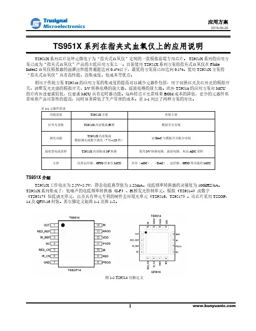
功能需求TS951X方案传统方案红外光切换TS951X内部集成H桥模拟开关实现调光功能TS951X内部集成模拟调光或数字调光(7位-128档)由DAC与模拟开关配合实现接收管电流采样TS951X内部集成I-F转换使用I-V转换电路、滤波电路,再由ADC采样主控仅需定时器、GPIO的8位MCU 具有(ADC)、(DAC)、定时器、GPIO等功能的MCUTS951X介绍TS951X工作电压为2.5V~5.5V,静态电流典型值为1.25mA。
电流频率转换器的灵敏度为100kHZ/uA。
TS951X系列集成了:低噪声的电流频率转换器(I-F)、H桥发光控制单元、模拟(TS9514)或数字(TS9517)恒流调光单元,以及具有坤元专利的硬件去环境光单元(TS9516、TS9517)。
该芯片采用TSSOP-14及QFN-16封装。
其引脚定义如图1-1及图1-2。
图1-1 TS9514引脚定义图1-1 TS9517引脚定义图1-3显示了TS9514的应用方案,TS9514的IR与RED引脚连接了红光LED以及红外LED,两只LED反向并联,IN以及ANOD连接一只光电二极管。
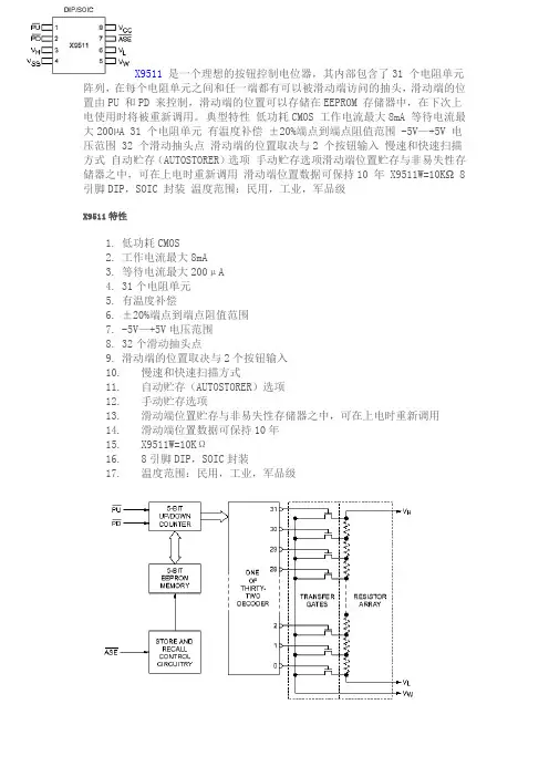
X9511是一个理想的按钮控制电位器,其内部包含了31 个电阻单元阵列,在每个电阻单元之间和任一端都有可以被滑动端访问的抽头,滑动端的位置由PU 和PD 来控制,滑动端的位置可以存储在EEPROM 存储器中,在下次上电使用时将被重新调用。
典型特性低功耗CMOS 工作电流最大8mA 等待电流最大200µA 31 个电阻单元有温度补偿±20%端点到端点阻值范围 -5V—+5V 电压范围 32 个滑动抽头点滑动端的位置取决与2 个按钮输入慢速和快速扫描方式自动贮存(AUTOSTORER)选项手动贮存选项滑动端位置贮存与非易失性存储器之中,可在上电时重新调用滑动端位置数据可保持10 年 X9511W=10KΩ 8 引脚DIP,SOIC 封装温度范围:民用,工业,军品级
X9511特性
1.低功耗CMOS
2.工作电流最大8mA
3.等待电流最大200μA
4.31个电阻单元
5.有温度补偿
6.±20%端点到端点阻值范围
7.-5V—+5V电压范围
8.32个滑动抽头点
9.滑动端的位置取决与2个按钮输入
10.慢速和快速扫描方式
11.自动贮存(AUTOSTORER)选项
12.手动贮存选项
13.滑动端位置贮存与非易失性存储器之中,可在上电时重新调用
14.滑动端位置数据可保持10年
15.X9511W=10KΩ
16.8引脚DIP,SOIC封装
17.温度范围:民用,工业,军品级
X9511 典型应用
1.家庭影院系统
2.电子保健产品
3.电话机,有线电视设备,无绳电话X9511 订购信息
X9511 应用电路。

Single Digitally-Controlled (XDCP™ ) Potentiometer (Push Button Controlled)FEATURES•Push button controlled •Low power CMOS—Active current, 3mA max —Standby current, 200µA max •31 resistive elements—Temperature compensated— ± 20% end to end resistance range —–5V to +5V range •32 wiper tap points—Wiper positioned via two push button inputs —Slow & fast scan modes —AUTOSTORE ® option —Manual store option—Wiper position stored in nonvolatile memory and recalled on power-up•100 year wiper position data retention •X9511W = 10K Ω •Packages—8-lead PDIP —8-lead SOICDESCRIPTIONThe Xicor X9511 is a push button controlled potentiom-eter that is ideal for push button controlled resistance trimming.The X9511 is a resistor array composed of 31 resistive elements. Between each element and at either end are tap points accessible to the wiper element. The position of the wiper element is controlled by the PU and PD inputs. The position of the wiper can be automatically stored in E 2 memory and then be recalled upon a sub-sequent power-on operation.The resolution of the X9511 is equal to the maximum resistance value divided by 31. As an example, for the X9511W (10K Ω ) each tap point represents 323 Ω .All Xicor nonvolatile products are designed and tested for applications requiring extended endurance and data retention.X9511AUTOSTORE is a registered trademark of Xicor, Inc.Terminal Voltage ±5V, 32 TapsX9511PIN DESCRIPTIONSV H/R H and V L/R LThe high (V H/R H) and low (V L/R L) terminals of the X9511 are equivalent to the fixed terminals of a mechanical potentiometer. The minimum voltage is –5V and the maximum is +5V. It should be noted that the terminology of V L/R L and V H/R H reference the relative position of the terminal in relation to wiper movement direction selected by the PU and PD inputs, and not the voltage potential on the terminal.PUThe debounced PU input is for incrementing the wiper position. An on-chip pull-up holds the PU input HIGH. A switch closure to ground or a LOW logic level will, after a debounce time, move the wiper to the next adjacent higher tap position.PDThe debounced PD input is for decrementing the wiper position. An on-chip pull-up holds the PD input HIGH. A switch closure to ground or a LOW logic level will, after a debounce time, move the wiper to the next adjacent lower tap position.ASEThe debounced ASE (AUTOSTORE enable) pin can be in one of two states:V IL—AUTOSTORE is enabled. When V CC powers down, an automatic store cycle takes place.V IH—AUTOSTORE is disabled. A LOW to HIGH will ini-tiate a manual store operation. This is for the user who wishes to connect a push button switch to this pin. For every valid push, the X9511 will store the current wiper position to the EEPROM.PIN CONFIGURATION PIN NAMESDEVICE OPERATIONThere are three sections of the X9511: the input control, counter and decode section; the EEPROM memory; and the resistor array. The input control section operates just like an up/down counter. The output of this counter is decoded to turn on a single electronic switch, connecting a point on the resistor array to the wiper output. Under the proper conditions the contents of the counter can be stored in EEPROM memory and retained for future use. The resistor array is comprised of 31 individual resistors connected in series. At either end of the array and between each resistor is an electronic switch that trans-fers the potential at that point to the wiper.The X9511 is designed to interface directly to two push button switches for effectively moving the wiper up or down. The PU and PD inputs increment or decrement a 5-bit counter respectively. The output of this counter is decoded to select one of the thirty-two wiper positions along the resistive array. The wiper increment input, PU and the wiper decrement input, PD are both connected to an internal pull-up so that they normally remain HIG H. When pulled LOW by an external push button switch or a logic LOW level input, the wiper will be switched to the next adjacent tap position.Internal debounce circuitry prevents inadvertent switch-ing of the wiper position if PU or PD remain LOW for less than 40ms, typical. Each of the buttons can be pushed either once for a single increment/decrement or continuously for a multiple increments/decrements. The number of increments/decrements of the wiper position depend on how long the button is being pushed. When making a continuous push, after the first second, the increment/decrement speed increases. For the first second the device will be in the slow scan mode. Then if the button is held for longer than 1 second the device will go into the fast scan mode. As soon as the button is released the X9511 will return to a standby condition.V H V CCPU PD 12348765X9511DIP/SOICV SS ASEV LV WSymbol DescriptionV H/R H High TerminalV W/R W Wiper TerminalV L/R L Low TerminalV SS GroundV CC Supply VoltagePU Push Up InputPD Push Down InputASE AUTOSTORE Enable InputX9511The wiper, when at either fixed terminal, acts like its mechanical equivalent and does not move beyond the last position. That is, the counter does not wrap around when clocked to either extreme.AUTOSTOREThe value of the counter is stored in EEPROM memory whenever the chip senses a power-down of V CC while ASE is enabled (held LOW). When power is restored, the content of the memory is recalled and the counter reset to the last value stored.If AUTOSTORE is to be implemented, ASE is typically hard wired to V SS. If ASE is held HIGH during power-up and then taken LOW, the wiper will not respond to the PU or PD inputs until ASE is brought HIG H and held HIGH.Manual (Push Button) StoreWhen ASE is not enabled (held HIGH) a push button switch may be used to pull ASE LOW and released to perform a manual store of the wiper position.R TOTAL with V CC RemovedThe end to end resistance of the array will fluctuate once V CC is removed.Figure 1. Typical circuit with ASE store pin controlled by push button switch Figure 2. Typical circuit with ASE store pin used in AUTOSTORE modeX9511ABSOLUTE MAXIMUM RATINGST emperature under bias....................–65°C to +135°C Storage temperature.........................–65°C to +150°C Voltage on PU, PD, and V CCwith respect to V SS..................................–1V to +7V Voltage on V H and V Lreferenced to V SS....................................–8V to +8V ∆V = |V H–V L|X9511W (10V)Lead temperature (soldering 10 seconds)..........300°C Wiper current............................................................±1mAANALOG CHARACTERISTICSElectrical CharacteristicsEnd-to-end resistance tolerance (20)Power rating at 25°CX9511W.........................................................10mW Wiper current .................................................±1mA Max. T ypical wiper resistance ...........................40Ω at 1mA T ypical noise............................< –120dB/√Hz Ref: 1VResolutionResistance ............................................................3% LinearityAbsolute linearity(1)............................................±1.0 Ml(2) Relative linearity(3).............................................±0.2 Ml(2)COMMENTStresses above those listed under “Absolute Maximum Ratings” may cause permanent damage to the device. This is a stress rating only; functional operation of the device (at these or any other conditions above those listed in the operational sections of this specification) is not implied. Exposure to absolute maximum rating conditions for extended periods may affect device reli-ability.Temperature Coefficient–40°C to +85°CX9511W......................................+300 ppm/°C T ypical Ratiometric temperature coefficient ................±20 ppm Wiper AdjustabilityUnlimited wiper adjustment.......(Non-Store operation) Wiper position store operations.......................100,000data changes Physical CharacteristicsMarking IncludesManufacturer’s T rademarkResistance Value or CodeDate CodeNotes:(1) Absolute linearity is utilized to determine actual wiper voltage versus expected voltage = (V w(n)(actual)–V w(n)(expected)) = ±1 Ml Maximum.(2) 1 Ml = Minimum Increment = R TOT/31.(3)Relative linearity is a measure of the error in step size between taps = V W(n+1)– [V w(n) + Ml] = +0.2 MlRECOMMENDED OPERATING CONDITIONS TemperatureMin.Max.Commercial 0°C +70°C Industrial–40°C+85°CSupply VoltageLimitsX95115V ±10%D.C. OPERATING CHARACTERISTICS (Over recommended operating conditions unless otherwise specified.)Notes:(4) T ypical values are for T A = 25°C and nominal supply voltage.(5) This parameter is periodically sampled and not 100% tested.A.C. OPERATING CHARACTERISTICS (Over recommended operating conditions unless otherwise specified.)POWER UP AND DOWN REQUIREMENTSThe are no restrictions on the sequencing of V CC and the voltage applied to the potentiometer pins during power-up or power-down conditions. During power-up, the data sheet parameters for the DCP do not fully apply until 1ms after V CC reaches its final value. The V CC ramp rate spec is always in effect.SymbolParameterLimitsUnitTest ConditionsMin.Typ.(4)Max.I CC V CC active current 13mA PU or PD held at V IL the other at V IH I SB Standby supply current100200µA PU = PD = V IH I LI PU, PD, ASE input leakage current 10µA V IN = V SS to V CCV IH PU, PD, ASE input HIGH voltage 2V CC + 1V V lL PU, PD, ASE input LOW voltage –10.8V R W Wiper resistance 40100ΩMax. Wiper Current ±1mAV VH VH terminal voltage –5+5V V VL VL terminal voltage–5+5V C IN (5)ASE, PU, PD input capacitance10pFV CC = 5V, V IN = 0V, T A = 25°C, f = 1MHzSymbolParameterLimitsUnit Min.Typ.(6)Max.t GAP Time between two separate push button eventsµst DB Debounce time3060ms t S SLOW After debounce to wiper change on a slow mode 100250375ms t S FAST (7)Wiper change on a fast mode 255075mst PU (7)Power up to wiper stable 500µst R V CC (7)V CC power-up rate 0.250mV/µs t ASTO (7)AUTOSTORE cycle time 2ms V ASTH (7)AUTOSTORE threshold voltage 4V V ASEND (7)AUTOSTORE cycle end voltage3.5VAUTOSTORE Cycle Timing DiagramNotes:V ASTH—AUTOSTORE threshold voltageV ASEND—AUTOSTORE cycle end voltaget ASTO—AUTOSTORE cycle time(6)T ypical values are for T A = 25°C and nominal supply voltage.(7)This parameter is periodically sampled and not 100% tested.Slow Mode TimingNote:(1) MI in the A.C. timing diagram refers to the minimum incremental change in the wiper voltage.Fast Mode TimingNote:(1) MI in the A.C. timing diagram refers to the minimum incremental change in the wiper voltage.PACKAGING INFORMATIONNOTE:1.ALL DIMENSIONS IN INCHES (IN PARENTHESES IN MILLIMETERS)2.PACKAGE DIMENSIONS EXCLUDE MOLDING FLASH8-Lead Plastic Dual In-Line Package Type PMax.PACKAGING INFORMATION8-Lead Plastic Small Outline Gull Wing Package Type SNOTE: ALL DIMENSIONS IN INCHES (IN PARENTHESES IN MILLIMETERS)LIMITED WARRANTY Devices sold by Xicor, Inc. are covered by the warranty and patent indemnification provisions appearing in its T erms of Sale only. Xicor, Inc. makes no warranty,express, statutory, implied, or by description regarding the information set forth herein or regarding the freedom of the described devices from patent infringement.Xicor, Inc. makes no warranty of merchantability or fitness for any purpose. Xicor, Inc. reserves the right to discontinue production and change specifications and prices at any time and without notice.Xicor, Inc. assumes no responsibility for the use of any circuitry other than circuitry embodied in a Xicor, Inc. product. No other circuits, patents, or licenses are implied.TRADEMARK DISCLAIMER:Xicor and the Xicor logo are registered trademarks of Xicor, Inc. AutoStore, Direct Write, Block Lock, SerialFlash, MPS, and XDCP are also trademarks of Xicor, Inc. All others belong to their respective owners.U.S. PATENTSXicor products are covered by one or more of the following U.S. Patents: 4,326,134; 4,393,481; 4,404,475; 4,450,402; 4,486,769; 4,488,060; 4,520,461; 4,533,846;4,599,706; 4,617,652; 4,668,932; 4,752,912; 4,829,482; 4,874,967; 4,883,976; 4,980,859; 5,012,132; 5,003,197; 5,023,694; 5,084,667; 5,153,880; 5,153,691;5,161,137; 5,219,774; 5,270,927; 5,324,676; 5,434,396; 5,544,103; 5,587,573; 5,835,409; 5,977,585. Foreign patents and additional patents pending.LIFE RELATED POLICYIn situations where semiconductor component failure may endanger life, system designers using this product should design the system with appropriate error detection and correction, redundancy and back-up features to prevent such an occurrence.Xicor’s products are not authorized for use in critical components in life support devices or systems.1.Life support devices or systems are devices or systems which, (a) are intended for surgical implant into the body, or (b) support or sustain life, and whose failure toperform, when properly used in accordance with instructions for use provided in the labeling, can be reasonably expected to result in a significant injury to the user.2. A critical component is any component of a life support device or system whose failure to perform can be reasonably expected to cause the failure of the lifesupport device or system, or to affect its safety or effectiveness.©Xicor, Inc. 2000 Patents PendingORDERING INFORMATIONX9511XXXTemperature RangeBlank = Commercial = 0°C to +70°C I = Industrial = –40°C to +85°C PackageP = 8-Lead Plastic DIP S = 8-Lead SOIC End to End Resistance W = 10K Ω。
调频收音机摘要:本调频收音机的设计是以SONY公司FM/ AM 收音机集成芯片CXA1238为核心,完成混频、中放,鉴频,功放等功能; 采用锁相环式频率合成器技术,实现回路的调谐与高度稳定的本振;采用RAM 实现电台存储;通过DC - DC 直流变换器实现全电路3V 供电;通过D/ A 输出控制电压, 键盘显示电路,从而实现多种程控搜索、电台存储,载波显示,时钟的控制及显示;利用片内电子音量控制功能,使输出音量得到了提升;为提高灵敏度,抑制噪声,增加了调频静噪调谐电路,使该收音机的收音质量得到了很大改善。
关键词:调频收音机;设计;控制一、方案设计和论证总体思路:收音电路以超大规模AM/FM立体声收音集成芯片为主体,本振频率可变,实现超外差式接收。
本振可变采用数字频率合成技术,由变容二极管和集成压控振荡器芯片实现振荡频率的电压控制;加入由频率合成芯片、高速分频器、运算放大器和晶体振荡器等组成的数字锁相环路,使输出频率稳定度达到与参考晶振同等水平;后级通过滤波及功率放大,使语音信号更清晰。
(一)接收芯片的选择方案一:采用CXA1019作为接收机电路的核心IC。
CXA1019是日本索尼公司研制的单片大规模接收机电路,它包含了AM/FM收音机从天线输入、高频放大、混频、本振到中频放大、检波直至低频(音频)功率放大的所有功能。
除此之外,还具有调谐指示,电子音量控制等一些辅助功能。
方案二:采用CXA1238作为接收机电路的核心IC。
CXA1238是索尼公司在20世纪80年代后期正式推出的集调幅、调频、锁相环、立体声解码等电路为一体的AM/FM立体声收音集成电路。
它的电源电压适应范围宽:2~10V范围内电路均能正常工作,且具有立体声和调谐指示LED驱动电路以及FM静噪功能等。
论证:上述两种方案实现的功能基本相同,但CXA1238内部带解调电路,可以对语音及数据调制后的信号进行解调,具有耗电小、调整简单等优点;且它的宽电压适应范围和立体声指示及静噪功能也是CXA1019所力所不能及的。
有关数字电位器X9511-14几个应用问题的探讨摘要:介绍按钮式数字电位器的防抖动和重复动作问题的一种解决方法,以及对数字电位器电压、电流、级数扩展问题的常见解决方法。
1 引言数字电位器以其调节准确方便,使用寿命长,受物理环境影响小,性能稳定等特点,已被广大电子工程技术人员所认识。
在数字电位器的家族中,X9511/14以其可用按钮直接控制的特点尤其受到青睐,本文欲针对应用开发人员对X9511/14在按钮控制过程中所出现的防抖动、和重复动作问题以及数字电位器通常遇到的问题作一简要探讨。
2 数字电位器简介数字电位器是可用数字信号控制电位器滑动端位置的新型器件。
一般分按钮控制和串行信号控制两种,下面以美国XICOR公司非易失性按钮控制数字电位器X9511为例简略介绍一下其原理。
X9511是数字电位器家族中的一种具有按钮控制,线性输出特点的产品,内部包含了31个电阻单元,32档输出滑动端,滑动端由输入到、引脚的负脉冲控制它向VH或VL端滑动。
滑动端位置可以被存储在非易失性的存储器EEPROM中,使其上电后能够自动恢复到原来的位置。
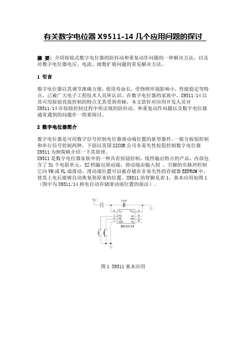
X9511的管脚见表1,基本应用如图1(图中为X9511/14掉电自动存储滑动端位置的接法)。
图1 X9511基本应用3 数字电位器在应用中经常遇到的问题数字电位器在我国还是近几年出现的新型器件,许多人在实际应用中对其不够了解,从而出现许多疑问,下面就经常出现的三个问题略作探讨。
按钮控制的数字电位器常出现按钮按下次数及输出值与预测值不符。
数字电位器本身能够承受的电流和电压有限,需要扩展。
在实际应用中数字电位器的阻值范围及分辨率不够,需要扩展。
3.1 按钮控制数字电位器的防抖动和重复触发问题上面的第一个问题所说按钮控制电位器的按键次数及输出值与预测不符,通常是其中某一档出现了重复触发动作,自然其按键次数和输出电位就会与预测值不符。
出现这种现象的原因常是用了面包板做试验,或是使用了劣质按钮,造成接触不良,线路噪声加剧,或是人为按钮动作不规范引起。
国产数字电位器芯片国产数字电位器芯片是一种用于调节电阻值的电子元件,具有数字控制和调节的功能。
它可以广泛应用于各种电子设备和系统中,如音频设备、通信设备、电源管理系统等。
本文将介绍国产数字电位器芯片的原理、特点以及应用领域。
一、国产数字电位器芯片的原理国产数字电位器芯片采用了先进的数字控制技术,通过数字输入信号控制电阻值的变化。
其内部结构由电阻网络和数字控制逻辑电路组成。
电阻网络由多个电阻单元串联或并联而成,通过控制逻辑电路对电阻单元的开关状态进行控制,从而实现电阻值的调节。
数字控制逻辑电路接收来自外部的数字输入信号,将其转换为控制信号,然后控制电阻单元的开关状态。
开关状态的改变会导致电阻值的变化,从而实现对电阻值的精确控制。
国产数字电位器芯片通常采用二进制编码方式进行控制,可以实现较高的分辨率和精度。
二、国产数字电位器芯片的特点1. 精确控制:国产数字电位器芯片具有较高的分辨率和精度,可以实现对电阻值的精确控制。
通过数字输入信号,可以实现微小电阻值的调节,满足不同应用的需求。
2. 可编程性:国产数字电位器芯片具有可编程性,可以通过编程或配置寄存器实现不同的电阻值和控制方式。
这使得它在不同的应用场景中具有更大的灵活性和适应性。
3. 低功耗:国产数字电位器芯片采用先进的低功耗技术,具有较低的功耗。
这使得它适用于一些对功耗要求较高的应用场景,如便携式设备和电池供电系统。
4. 高可靠性:国产数字电位器芯片具有良好的可靠性和稳定性,能够在各种环境条件下正常工作。
其内部采用了可靠的材料和工艺,经过严格的生产测试和质量控制,保证了产品的性能和可靠性。
三、国产数字电位器芯片的应用领域1. 音频设备:国产数字电位器芯片可以用于音频设备中的音量控制和音调调节。
通过数字控制,可以实现音频信号的精确调节,提高音频系统的性能和音质。
2. 通信设备:国产数字电位器芯片可以用于通信设备中的增益控制和衰减控制。
通过数字控制,可以实现信号的精确调节,提高通信系统的灵敏度和抗干扰能力。
数字电位器芯片X9511的应用扩展引言数字电位器在我国还是近几年出现的新型器件,该器件一出现,就以其调节准确方便,使用寿命长,受物理环境影响小,性能稳定等特点,而被广大电子工程技术人员所接受。
但数字电位器本身能够承受的电流和电压有限,因而需要扩展,同时在实际应用中,数字电位器的阻值范围及分辨率也需要扩展,本文介绍的扩展方案适用于各种信号的数字电位器。
数字电位器简介数字电位器是可用数字信号控制电位器滑动端位置的新型器件,一般分按钮控制和串行信号控制两种,X9511就是X I C O R公司生产的理想按键式数字电位器,它内含31个串联电阻阵列和32个轴头。
轴头位置由两个按键控制,并且可以被存储在一个E2P R O M存储器中,以供下一次通电时重新调用,并自动恢复轴头位置,X9511有1kΩ和10kΩ的X9511Z和X9511W两种规格。
X9511内部由计数器、存储器、译码器、模拟开关和电阻阵列等电路组成,其中计数器是5位可逆计数器,可用于对控制信号P U(或P D)进行加(或减)计数,计数器的计数值可以在A S E的控制下存储非易失性存储器中。
计数器的数值经过32选1译码器译码后可用于控制模拟开关,32个模拟开关相当于电位器的32个轴头,电阻阵列由采用集成电路工艺制作的31个串联一起的电阻构成,电阻两端分别连接模拟开关的一端,而模拟开关的另一端连接在一起构成数字电位器的滑动端(V W),译码器的输出端可控制模拟开关的通断,从而实现滑动轴头位置的变化。
X9511的计数器电路具有以下特点:◆ 输入端具有内部上拉电阻和消除开关抖动的抗扰电路,当输入脉冲宽度小于40m s时,计数器将其视为干扰信号而不进行计数;◆ P U和P D引脚可直接连接一个按钮开关到地,当按钮按下时,在P U或P D端产生一个负脉冲,使计数器进行加1(按P U键)或减1(按P D键)计数;◆ 能将计数值存储在非易失性存储器E2P R O M中长期保存;◆ 能在上电时自动将E2P R O M中的数据恢复到计数器中;◆ 当计数器计数到最大值“31”时,P U按键失效,而计数到最小值“0”时,P D按键失效,从而避免循环计数,保证电位器调到最大位置时不会跳到零位,或从零位跳到最大位置。
摘要本设计介绍了用FPGA对信号发生器进行控制的函数发生器,然后经功率放大器使之产生固定要求的电磁场来清除水垢。
水垢分解的常用方法是利用电磁场,电磁场吸附正负离子,使之分解。
水垢处理的频率在2MHZ到20MHZ范围内。
MAX038具有可调频率特性,其频率范围为1HZ到20MHZ。
满足要求,其还具有占空比可调等优点。
MAX038与FPGA的连接用X9313数控电位器。
实现了数字与模拟的转换。
因功放电路带宽等要求,功率放大器不能用集成来实现,所以用分立元器件搭建的电路。
主要的电路部分是MAX038与FPGA连接的模块。
其全部电路图均用DXP软件来做。
功率放大部分,因为其没有专门的高频率高瓦数的集成元件,抗干扰差和其他不利因素等影响,就会使功率放大器失真。
关键词:MAX038 ;X9313 ;DXPAbstractThis subject introduces signal Generator, function generator,The subject describes the function generator with the control of Signal Generator at FPGA. Through the Generated of the power amplifier ,we need a fixed magnetic field to Clear scale. There are several common methods of the Scale decomposition:The first is the use of electric field. The scale cans decomposition in Adsorption of positive and negative electromagnetic fields. the frequency of the scale cleaning 2MHZ to 20MHZ. MAX038 owes the features of adjustable frequency. The frequency‗s range is between 1HZ and 20MHZ. In order to meet the requirements, he has the advantage of adjustable duty cycle. Connect Digital power controller named X9313 with MAX038 and FPGA. It achieves the digital and analog conversion. Bandwidth requirements for power amplifier, power amplifier cannot be used to achieve integration, so the circuit built using discrete components. The major part of the circuit is connected with the FPGA module. All of its circuits are to do with the DXP software. There is no specific integration of high frequency high wattage components, so interference and other adverse factors such as poor impact; it will make power amplifier distortion.Key words: MAX038; X9511; DXP目录1 引言 (1)1.1 科学意义和社会应用前景 (1)1.2 国内外研究概况、水平和发展趋势 (1)1.3 高频的基本原理 (2)2 总体设计原理 (4)2.1水垢生产的机理 (4)2.2 清除水垢方法 (4)2.3 设计原理 (5)3 高频信号发生器设计 (6)3.1 DXP软件介绍 (6)3.2 设计指标 (6)3.3 方案论证与比较 (7)3.4 MAX038芯片介绍 (8)3.4.1 MAX038简介 (8)3.4.2 芯片引脚 (8)3.4.3 MAX038 内部电路图 (9)3.5 频率、幅值及占空比控制 (10)3.6 芯片X9511介绍 (11)3.7 正弦波发生器设计 (13)3.8 正弦波电路PCB和示波器波形 (14)4 功率放大器设计 (17)4.1 常见功放种类 (17)4.2 功放的输出 (18)4.2.1 定阻式输出 (18)4.2.2 定压式输出 (18)4.3 功率放大器的组成 (18)4.4 功率放大器原理 (18)4.5 功率放大器电流的特点 (20)4.6 功率放大器术语 (21)4.6.1 工作范围 (21)4.6.2 传输增益 (21)4.6.3 输出功率 (21)4.7 功放设计 (21)4.7 功放电路及PCB (22)4.8 功放仿真 (23)5 控制电路设计 (24)5.1 电路功能 (24)5.2 HDL仿真 (24)5.3.1 FPGA介绍 (24)5.3.2、设计流程 (25)总结 (26)致谢 (27)参考文献 (28)附录A 英文原文 (29)附录B 英文翻译 (38)附录C 电路图 (46)1 引言1.1 科学意义和社会应用前景随着高科技工业的发展和生活水准的提高,各类水系统越来越广泛应用于工业生产及民用生活方面,如锅炉,热交换器,中央空调,循环冷却水系统等。
国产数字电位器芯片
1 中国开发的数字电位器芯片
近几年,中国芯片行业取得了突飞猛进的发展,已经大大改变了
芯片行业的格局。
尤其是随着5G通信技术的普及,电子芯片应用也逐
渐普遍。
其中,数字电位器亦即准确度可达0.1°的精密可调电位器,目前已是电子产品众多应用中不可或缺的组成部分。
随着新能源汽车、自动驾驶、智能家居等领域带来的爆发式增长,对于数字电位器零部件的需求也随之剧增,造成了行业供应紧张现象,中国相关厂商迫切需要有一种解决方案来满足行业的供需关系。
为此,上海产研所投入大量研发力量,以满足电子零部件行业中
高端可调电位器的需求。
该机构研发出的数字电位器芯片,以行业领
先的准确度、落后的低静态目标、多段精度和强大的环境适应能力为
特色,支持40 °C至85 °C的工作温度,不仅助力新能源汽车、智
能家居等相关众多应用领域,还为电子产品提供了更优质的可调控性能。
无论是丰富的I/O配置,还是新能源、智能家居、安防和医疗等
领域对准确度和低功耗的要求,上海产研所的数字电位器芯片都做到
了完美结合。
普及度更是比普通的商用级可调电位器产品更加显著,
为芯片行业提供了一条新的发展道路,能够更好地满足全球电子产品
行业的需求。
而在该芯片的研发过程中,上海产研所的研发团队也从中吸取宝贵的经验,这将有助于其在特定市场和行业的自主研发能力。
由此,成为未来芯片行业发展的引擎,使得中国芯片行业自主创新,贡献芯片创新产业的发展和创新动能,推动中国芯片行业向更优质的体现。
国产数字电位器芯片在日新月异的科技发展时代,芯片作为一种重要的电子元件,得到了越来越多的应用。
近几年,国产数字电位器芯片也开始被广泛应用,这种芯片可以为电子设备提供更多的功能和更高的性能,从而更好地满足用户的多样化需求。
国产数字电位器芯片的基本原理是:电子芯片通过精密的电子元件和组件来实现,它是一种数字化的电子元件,可以通过软件来实现电路控制。
数字电位器芯片具有多种功能,可以控制电路的总体变化,控制电路的智能柔韧化,以及实现电路的更精细的控制。
该芯片具有多种优势:它可以提高系统的可靠性,提高电路的效率,减少系统损耗,减少系统介质的消耗,节省空间,节省能耗等。
国产数字电位器芯片的发展为电子设备的发展带来了新的机遇,尤其在汽车电子设备、移动通信设备、家用电器等领域的发展中,得到了广泛的应用。
该芯片在汽车电子设备中可提高系统可靠性、提高安全性和降低故障率;在移动通信设备中可提高传输速率;在家用电器中可降低电子消耗,提高效率,延长使用寿命等。
另外,国产数字电位器芯片还可以用于医疗设备、航空、工业自动化等领域,可以更高效地控制系统,达到精确控制的要求,可以有效提高系统的安全性和可靠性。
当前,国产数字电位器芯片的研发正在飞速发展,相关技术也是如雨后春笋般蓬勃发展。
为了让消费者能够得到更好的体验,可靠的产品也应该强调可靠性,并加以保障。
此外,对于研发、生产、营销、服务等环节,还应该加强国产产品的市场竞争力,努力提升企业的核心竞争力,才能让国产数字电位器芯片在市场上受到更多青睐。
综上所述,国产数字电位器芯片在当下已经被广泛应用,它不仅可以为电子设备提供更多的功能,还可以提高更高的性能,节省能耗,提高系统的可靠性。
未来,国产数字电位器芯片将会发挥更大的作用,但要想让它发挥出最大作用,就必须保障产品可靠性,加强市场竞争力,努力提升企业的核心竞争力。
嵌入式常用IC芯片1.电源变换IC芯片7800 三端,固定正电压输出稳压器(块)芯片7900 三端,固定负电压输出稳压器(块)芯片AD580 三端,精密电压基准芯片ADR290/291/292/293 高精度,新型XFET 3端基准电源芯片D14,D24 DC-DC隔离电源模块HV-2405E 50mA,5~24V,AC/DC电源IC芯片HQA-2405E AC/DC电源变换器模块IMP706 低功耗,uP电源监控IC芯片LM117/217/317 3端,可调正电压输出稳压芯片LM137/237/337 3端,可调负电压输出稳压(块)芯片LM138/238/338 3端,大电流,可调正电压输出稳压(块)芯片LM150/250/350 3端,大电流,可调正电压输出稳压(块)芯片LM2930 汽车用3端稳压器芯片LT108X/SP116XX 3端,低电压,输出可调稳压器芯片M5236L/37L 灵活方便,低电压差,3端稳压驱动芯片MAX610 无变压器式,AC/DC电源变换器IC芯片MAX619 输入2V,输出5V,充电泵DC/DC变换器IC芯片MAX629 DC/DC转换芯片MAX638 过低电压检测报警,降压开关型,DC/DC电源变换器IC芯片MAX639 过低电压检测报警,降压开关型,DC/DC电源变换器IC芯片MAX682-685 低电压差,微功耗稳压器芯片MAX706 电压监控芯片MAX813L 看门狗,电压监控芯片MAX889 2MHZ稳压型电荷泵,负电压输出,DC/DC变换器芯片MAX1606 输入5V,输出28V,LCD偏置电源DC/DC芯片MAX1642/1643 输入电压仅为1V的DC/DC变换器芯片MAX1692 1.8V,降压型,微型开关,DC/DC芯片MAX1725/1726 更低功耗,低压差,线性稳压器芯片MAX1742/1842 内含1A开关,1MHz,降压型DC/DC芯片MAX1744/1745 36V输入,10W输出,降压型转换器芯片MAX1730/1759 稳压型,电荷泵,DC/DC芯片MAX1775 双路,降压型,2A以上,DC/DC芯片MAX1832/1833/1834/1835 电池反接保护,升压型DC/DC转换器芯片MAX1864/1865 降压型,DC/DC,5路输出线缆MODEM电源芯片MAX5130+PIC 精确可编程,8000基准电压值,DC/DC发生器芯片MAX6125 微封装,微功耗,微漂移,DC/DC芯片MAX6129 功耗更低,串联型,3端,电压基准芯片MAX6333 监视电压可低至1.6V的新型单片复位IC芯片MAX6821-6825 手动复位,“看门狗”定时器,低功耗,UP监控电路芯片MAX828/829 充电泵,反压型,DC/DC芯片MAX8880/8881 带有电源好2(POWDWR-OK)输出的DC/DC芯片MAX8883 双路,低压差,线性稳压器芯片MC1403 8脚精密电压基准芯片MIC2141 微功耗,升压型,V0可控,DC/DC变换器芯片PS0500-5 500mA,超小型,AC/DC电源变换芯片TOP1xx-2xx 无变压器,5W以上,AC/DC变换式精密开关电源IC芯片TL499AC 可调线型串联稳压器和升压型开关稳压器(合成稳压器)芯片TPS7350 5V固定输出,掉电延时复位,低压差稳压器芯片W431 3端,可调式电压基准芯片YA-S AC/DC电源变换器模块2.数字温度传感器AD526 增益可编程运算放大器芯片AD620 低功耗,高精密度仪器用运放芯片AD623 单电源Rail-Rail仪表运放芯片AD625 增益可编程运算放大器芯片AD626 单电源差分运算放大器芯片AD7416 带IIC接口,10位低功耗数字温度传感器芯片AD8571/8572/8574 0温漂,单电源,运算放大器芯片AD8591/8592/8594 带节能控制端的CMOS,单电源工作,满电源输入输出,运算放大器芯片DS1620 数字式温度传感器IC芯片DS1621 数字式温度传感器IC芯片及恒温控制器IC芯片DS1625 数字温度计和控温器芯片DS1629 2线接口,带有实时时钟的温度传感器芯片DS1820 数字式温度传感器IC芯片ITT2301AF 射频功率放大器芯片LM76 带数字温度传感器,IIC总线接口,12位信号输出,测温芯片LM92 数字式温度传感器芯片MAX54xx 体积更小,256级,数字电位器芯片MAX4265~4270 超低失真,单+5V,300MHz,运算放大器芯片MAX4430/4431/4432/4433 高速(280MHz),高精度,宽频带,单/双运算放大器芯片MAX6627/6628 兼容SPI接口的远端结温检测器芯片MAX6629/6630/6631/6632 微型SOT封装,+-1摄氏度精度的数字温度传感器芯片MAX6657/6658/6659 +-1摄氏度的本地和远端结温检测器芯片OP193/293/493 精密,微功耗,运算放大器芯片OP177 超精密运算放大器芯片OP777 精密,微功耗,单电源,运算放大器芯片MIC91x 高速(100~350MHz)运算放大器芯片X9241 IIC接口,数字电位器(EEPOT)IC芯片X9312 数字电位器IC芯片X9313 数控电位器芯片X9511 PushPOT按钮控制电位器芯片3.电机控制及驱动芯片87C196MC 电机控制专用微处理器芯片CIPH9803 可编程步进电机控制IC芯片FR-Z240-7.5K 变频调速器芯片HEF4752V PWM大规模集成电路芯片IR2110 高压浮动MOSFET,栅极步进电机驱动器IC芯片LM628 直流电机运动控制芯片LM1542 无刷直流电机控制器芯片LMD18200 H桥组件电机驱动芯片MA818 3相PWM,变频调速专用控制器芯片MAX1749 微型直流电机驱动控制芯片MC33033 带温度补偿的直流电机控制器芯片ML4428 无传感器PWM,无刷直流电机控制器芯片MOC30xx 双向晶闸管电机控制驱动器(双向光电耦合器)IC芯片MTE1122 智能型电机驱动运放芯片PA03 大功率(1000w)运放电机驱动芯片PA21/25/26 双功率电机驱动运放芯片PA61 大功率运放电机驱动芯片PA85 高压,高速,大功率,运放驱动芯片PBL3772/PBM3960 高性能步进电机驱动IC芯片组PH2083 多模式步进电机控制器IC芯片PMM8713 步进电机专用控制芯片SA06 脉宽调制运放,电机驱动芯片SA60 脉宽调制型功放芯片SA866 可编程,全数字化,3相PWM,变频调速控制器IC芯片ST6210 通用电机驱动电路(MCU)IC芯片TDA1085C 通用电机速度控制器芯片UCx637XC9536 PWM型直流电机驱动芯片XC9536 步进电机CPLD控制芯片4.数字通信IC芯片及接口5G16C550ACM1330E/1550DACMTX16/ACMRX18ADM101EAM7910Core 01DS14C232C/232TDS26F31DS26C32DS3695/3696/3697/3698DS8921DS8922DS9637DS9638DS14185DS75176DS96172/96174DS96173/96175HT9200AICL232KX50xxLM1893LMx3162M303S/303RM-8888MAX48x/49xMAX202MAX202E/211E/213E/232E/241EMAX214MAX220/232/232AMAX250/251MAX1480A/1480BMAX3080E-3089EMAX3082MAX3100MAX3140MAX3222/3232MAX3224~3227MAX3238E/3248E常用集成电路功能简介型号功能简述1710 视频信号处理集成电路2274 延迟集成电路2800 红外遥控信号接收集成电路4094 移位寄存串入、并出集成电路4260 动态随机存储集成电路4464 存储集成电路4558 双运算放大集成电路5101 天线开关集成电路15105 充电控制集成电路15551 管理卡升压集成电路31085 射频电源集成电路74122 可重触发单稳态集成电路85712 场扫描信号校正处理集成电路85713 行扫描信号校正集成电路0206A 天线开关集成电路03VFG9 发射压控振荡集成电路1021AC 发射压控振荡集成电路1097C 升压集成电路140N 电源取样比较放大集成电路14DN363 伺服控制集成电路1N706 混响延时集成电路20810-F6096 存储集成电路2252B 微处理集成电路24C01ACEA 存储集成电路24C026 存储集成电路24C04 存储集成电路24C64 码片集成电路24LC16B 存储集成电路24LC65 电可改写编程只读存储集成电路27C1000PC-12 存储集成电路27C2000QC-90 存储集成电路27C20T 存储集成电路27C512 电可改写编程只读存储集成电路28BV64 码片集成电路28F004 版本集成电路32D54 电源、音频信号处理集成电路32D75 电源、音频信号处理集成电路32D92 电源中频放大集成电路4066B 电子开关切换集成电路424260SDJ 存储集成电路4270351/91B9905 中频放大集成电路4370341/90M9919 中频处理集成电路4580D 双运算放大集成电路47C1638AN-U337 微处理集成电路47C1638AU-353 微处理集成电路47C432GP 微处理集成电路47C433AN-3888 微处理集成电路49/4CR1A 中频放大集成电路5G052 发光二极管四位显示驱动集成电路5G24 运算放大集成电路5W01 双运算放大集成电路649/CRIA70612 中频放大集成电路673/3CR2A 多模转换集成电路74HC04 逻辑与非门集成电路74HC04D 六反相集成电路74HC123 单稳态集成电路74HC125 端口功能扩展集成电路74HC14N 六反相集成电路74HC157A 多路转换集成电路74HC165 移相寄存集成电路74HC245 总线收发集成电路74HC32 或门四2输入集成电路74HC374八D 触发集成电路74HC573D 存储集成电路74HCT157 多路转换双输入集成电路74HCT4046A 压控振荡集成电路74HCT4538D 单稳态集成电路74HCT4538N 触发脉冲集成电路74HCT86D 异或门四2输入集成电路74HCU04 与非门集成电路74LS125 端口功能扩展集成电路74LS373 锁存集成电路74LS393 计数双四位二进制集成电路74LS74双D 触发集成电路78014DFP 系统控制处理集成电路811N 伴音阻容偏置集成电路83D33 压控振荡集成电路87C52 微处理集成电路87CK38N-3584 微处理集成电路87CK38N-3627 微处理集成电路89C52 系统控制处理集成电路89C55 系统控制处理集成电路93C66 电可改写编程只读存储集成电路93LC56 电可改写编程存储集成电路9821K03 系统控制集成电路A1642P 背景歌声消除集成电路A701 红外遥控信号接收集成电路A7950 场频识别集成电路A8772AN 色差信号延迟处理集成电路A9109 功率放大集成电路AAB 电源集成电路ACA650 色度信号解调集成电路ACFP2 色度、亮度信号分离集成电路ACP2371 多伴音、多语言改善集成电路ACVP2205 色度、亮度信号分离集成电路AD1853 立体声数/模转换集成电路AD1858 音频解调集成电路AD722 视频编码集成电路ADC2300E 音频数/模转换集成电路ADC2300J 音频数/模转换集成电路ADC2310E 音频数/模转换集成电路ADV7172 视频编码集成电路ADV7175A 视频编码集成电路AE31201 频率显示集成电路AJ7080 射频调制集成电路AK4321-VF-E1 音频数/模转换集成电路AN1319 双高速电压比较集成电路AN1358S 双运算放大集成电路AN1393 双运算放大集成电路AN1431T 稳压电源集成电路AN1452 音频前置放大集成电路AN1458S 双运算放大集成电路AN206 伴音中频及前置放大集成电路AN222 自动频率控制集成电路AN236 副载波信号处理集成电路AN239Q 图像、伴音中频放大集成电路AN247P 图像中频放大、AGC控制集成电路AN253P 调频/调幅中频放大集成电路AN262 音频前置放大集成电路AN2661NK 视频信号处理集成电路AN2663K 视频信号处理集成电路AN272 音频功率放大集成电路AN2751FAP 视频信号处理集成电路AN281 色度解码集成电路AN2870FC 多功能控制集成电路AN295 行、场扫描信号处理集成电路AN301 伺服控制集成电路AN305 视频自动增益控制集成电路AN306 色度自动相位控制集成电路AN318 直流伺服控制集成电路AN320 频率控制、调谐显示驱动集成电路AN3215K 视频信号处理集成电路AN3215S 视频信号处理集成电路AN3224K 磁头信号记录放大集成电路AN3248NK 亮度信号记录、重放处理集成电路AN331 视频信号处理集成电路AN3311K 磁头信号放大集成电路AN3313 磁头信号放大集成电路AN3321S 录像重放信号处理集成电路AN3331K 磁头信号处理集成电路AN3337NSB 磁头信号放大集成电路AN3380K 磁头信号处理集成电路AN3386NK 磁头信号处理集成电路AN3495K 色度、亮度信号降噪集成电路AN355 伴音中频放大、检波集成电路AN3581S 视频驱动集成电路AN366 调频/调幅中频放大集成电路AN3791 移位控制集成电路AN3792 磁鼓伺服控制接口集成电路AN3795 主轴伺服控制接口集成电路AN3814K 电机驱动集成电路AN4265 音频功率放大集成电路AN4558 运算放大集成电路AN5010 电子选台集成电路AN5011 电子选台集成电路AN5015K 电子选台集成电路AN5020 红外遥控信号接收集成电路AN5025S 红外遥控信号接收集成电路AN5026K 红外遥控信号接收集成电路AN5031 电调谐控制集成电路AN5034 调谐控制集成电路AN5036 调谐控制集成电路AN5043 调谐控制集成电路AN5071 频段转换集成电路AN5095K 电视信号处理集成电路AN5110 图像中频放大集成电路AN5130 图像中频、视频检波放大集成电路AN5138NK 图像、伴音中频放大集成电路AN5156K 电视信号处理集成电路AN5177NK 图像、伴音中频放大集成电路AN5179K 图像、伴音中频放大集成电路AN5183K 中频信号处理集成电路AN5195K 中频、色度、扫描信号处理集成电路AN5215 伴音信号处理集成电路AN5222 伴音中频放大集成电路AN5250 伴音中频放大、鉴频及功率放大集成电路AN5262 音频前置放大集成电路AN5265 音频功率放大集成电路AN5270 音频功率放大集成电路AN5273 双声道音频功率放大集成电路AN5274 双声道音频功率放大集成电路AN5275 中置、3D放大集成电路AN5285K 双声道前置放大集成电路AN5295NK 音频信号切换集成电路AN5312 视频、色度信号处理集成电路AN5313NK 视频、色度信号处理集成电路AN5342 图像水平轮廓校正集成电路AN5342FB 水平清晰度控制集成电路AN5344FBP 色度信号处理集成电路AN5348K 人工智能信号处理集成电路AN5385K 色差信号放大集成电路AN5410 行、场扫描信号处理集成电路AN5421 同步检测集成电路AN5422 行、场扫描信号处理集成电路AN5512 场扫描输出集成电路AN5515 场扫描输出集成电路AN5520 伴音中频放大及鉴频集成电路AN5521 场扫描输出集成电路AN5532 场扫描输出集成电路AN5534 场扫描输出集成电路AN5551 枕形校正集成电路AN5560 场频识别集成电路AN5600K 中频、亮度、色度及扫描信号处理集成电路AN5601K 视频、色度、同步信号处理集成电路AN5607K 视频、色度、行场扫描信号处理集成电路AN5615 视频信号处理集成电路AN5620X 色度信号处理集成电路AN5621 场扫描输出集成电路AN5625 色度信号处理集成电路AN5633K 色度信号处理集成电路AN5635 色度解码集成电路AN5635NS 色度解码集成电路AN5637 色度解码、亮度延迟集成电路AN5650 同步信号分离集成电路AN5682K 基色电子开关切换集成电路AN5693K 视频、色度、行场扫描信号处理集成电路AN5712 图像中频放大、AGC控制集成电路AN5722 图像中频放大、检波集成电路AN5732 伴音中频放大、鉴频集成电路AN5743 音频功率放大集成电路AN5750 行自动频率控制及振荡集成电路AN5757S 行扫描电源电压控制集成电路AN5762 场扫描振荡、输出集成电路AN5764 光栅水平位置控制集成电路AN5765 电源稳压控制集成电路AN5767 同步信号处理集成电路AN5768 光栅倾斜校正控制集成电路AN5769 行、场会聚控制集成电路AN5790N 行扫描信号处理集成电路AN5791 同步脉冲相位与脉宽调整集成电路AN5803 双声道立体声解调集成电路AN5836 双声道前置放大集成电路AN5858K 视频信号控制集成电路AN5862 视频信号控制集成电路AN5862S-E1 视频信号开关控制集成电路AN5870K 模拟信号切换集成电路AN5891K 音频信号处理集成电路AN614 行枕形校正集成电路AN6210 双声道前置放大集成电路AN6306S 亮度信号处理集成电路AN6308 模拟电子开关集成电路AN6327 视频重放信号处理集成电路AN6341N 伺服控制集成电路AN6342N 基准分频集成电路AN6344 伺服控制集成电路AN6345 分频集成电路AN6346N 磁鼓伺服控制集成电路AN6350 磁鼓伺服控制集成电路AN6357N 主轴接口集成电路AN6361N 色度信号处理集成电路AN6367NK 色度信号处理集成电路AN6371S 自动相位控制集成电路AN6387 电机伺服控制集成电路AN6550 卡拉OK音频放大集成电路AN6554 四运算放大集成电路AN6561 双运算放大集成电路AN6562SG 双运算放大集成电路AN6609N 电机驱动集成电路AN6612 电机稳速控制集成电路AN6650 电机速度控制集成电路AN6651 电机速度控制集成电路AN6652 电机稳速控制集成电路AN6875 发光二极管五位显示驱动集成电路AN6877 发光二极管七位显示驱动集成电路AN6884 发光二极管五位显示驱动集成电路AN6886 发光二极管五位显示驱动集成电路AN6888 发光二极管显示驱动集成电路AN6914 双电压比较集成电路AN7085N5 单片录、放音集成电路AN7105 双声道音频功率放大集成电路AN7106K 双声道音频功率放大集成电路AN7108 单片立体声放音集成电路AN710S 单片放音集成电路AN7110E 音频功率放大集成电路AN7114 音频功率放大集成电路AN7116 音频功率放大集成电路AN7118 双声道音频功率放大集成电路AN7118S 双声道音频功率放大集成电路AN7120 音频功率放大集成电路AN7124 双声道音频功率放大集成电路AN7145 双声道音频功率放大集成电路AN7148 双声道音频功率放大集成电路AN7158N 音频功率放大7.5W×2集成电路AN7161N 音频功率放大集成电路AN7164 双声道音频功率放大集成电路AN7171NK 音频功率放大集成电路AN7205 调频/调谐及高频放大集成电路AN7220 调频/调幅中频放大集成电路AN7222 调频/调幅中频放大集成电路AN7223 调频/调幅中频放大集成电路AN7226 调频/调幅中频放大集成电路AN7256 调频/调谐及中频放大集成电路AN7311 双声道前置放大集成电路AN7312 双声道前置放大集成电路AN7315 双声道前置放大集成电路AN7315S 双声道前置放大集成电路AN7320 音频前置放大集成电路AN7396K 双声道前置放大集成电路AN7397K 双声道前置放大集成电路AN7410 调频立体声多路解码集成电路AN7414 调频立体声解码集成电路AN7420N 调频立体声解码集成电路AN7470 调频立体声解码集成电路AN7805 三端电源稳压+5V/1A集成电路AN7806 三端电源稳压+6V/1A集成电路AN7807 三端电源稳压+7V/1A集成电路AN7808 三端电源稳压+8V/1A集成电路AN7809 电源稳压+9V/1A集成电路AN7810 三端电源稳压+10V/1A集成电路AN7812 三端电源稳压+12V/1A集成电路AN7815 三端电源稳压+15V/1A集成电路AN7818 三端电源稳压+18V/1A集成电路AN7820 三端电源稳压+20V/1A集成电路AN7824 三端电源稳压+24V/1A集成电路AN78L05 三端电源稳压+5V/0.1A集成电路AN78L06 三端电源稳压+6V/0.1A集成电路AN78L08 三端电源稳压+8V/0.1A集成电路AN78L09 三端电源稳压+9V/0.1A集成电路AN78L10 三端电源稳压+10V/0.1A集成电路AN78L12 三端电源稳压+12V/0.1A集成电路AN78L15 三端电源稳压+15V/0.1A集成电路AN78L18 三端电源稳压+18V/0.1A集成电路AN78L20 三端电源稳压+20V/0.1A集成电路AN78L24 三端电源稳压+24V/0.1A集成电路AN78M05 三端电源稳压+5V/0.5A集成电路AN78M06 三端电源稳压+6V/0.5A集成电路AN78M08 三端电源稳压+8V/0.5A集成电路AN78M09 三端电源稳压+9V/0.5A集成电路AN78M10 三端电源稳压+10V/0.5A集成电路AN78M12 三端电源稳压+12V/0.5A集成电路AN78M15 三端固定式稳压+15V/0.5A集成电路AN78M18 三端电源稳压+18V/0.5A集成电路AN78M20 三端电源稳压+20V/0.5A集成电路AN78M24 三端电源稳压+24V/0.5A集成电路AN7905 三端电源稳压-5V/1A集成电路AN7906 三端电源稳压-6V/1A集成电路AN7908T 三端电源稳压-8V/1A集成电路AN7909T 三端电源稳压-9V/1A集成电路AN7910T 三端电源稳压-10V/1A集成电路AN7912 三端电源稳压-12V/1A集成电路AN7915 三端电源稳压-15V/1A集成电路AN7918 三端电源稳压-18V/1A集成电路AN7920 三端电源稳压-20V/1A集成电路AN7924 三端电源稳压-24V/1A集成电路AN79L05 三端电源稳压-5V/0.1A集成电路AN79L06 三端电源稳压-6V/0.1A集成电路AN79L08 三端电源稳压-8V/0.1A集成电路AN79L09 三端电源稳压-9V/0.1A集成电路AN79L10 三端电源稳压-10V/0.1A集成电路AN79L12 三端电源稳压-12V/0.1A集成电路AN79L15 三端电源稳压-15V/0.1A集成电路AN79L18 三端电源稳压-18V/0.1A集成电路AN79L20 三端电源稳压-20V/0.1A集成电路AN79L24 三端电源稳压-24V/0.1A集成电路AN79M05 三端电源稳压-5V/0.5A集成电路AN79M06 三端电源稳压-6V/0.5A集成电路AN79M08 三端电源稳压-8V/0.5A集成电路AN79M09 三端电源稳压-9V/0.5A集成电路AN79M10 三端电源稳压-10V/0.5A集成电路AN79M12 三端电源稳压-12V/0.5A集成电路AN79M15 三端电源稳压-15V/0.5A集成电路AN79M18 三端电源稳压-18V/0.5A集成电路AN79M20 三端电源稳压-20V/0.5A集成电路AN79M24 三端电源稳压-24V/0.5A集成电路AN8028 自激式开关电源控制集成电路AN8270K 主轴电机控制集成电路AN8280 电机驱动集成电路AN8290S 主轴电机驱动集成电路AN8355S 条形码扫描接收集成电路AN8370S 光电伺服控制集成电路AN8373S 射频伺服处理集成电路AN8375S 伺服处理集成电路AN8389S-E1 电机驱动集成电路AN8480NSB 主轴电机驱动集成电路AN8481SB-E1 主轴电机驱动集成电路AN8482SB 主轴电机驱动集成电路AN8623FBQ 主轴伺服处理集成电路AN8788FB 电机驱动集成电路AN8802CE1V 伺服处理集成电路AN8813NSBS 主轴电机驱动集成电路AN8819NFB 伺服驱动、直流交换集成电路AN8824FBQ 前置放大集成电路AN8825NFHQ-V 聚焦、循迹误差处理集成电路AN8831SC 视频预视放集成电路AN8832SB-E1 射频放大、伺服处理集成电路AN8837SB-E1 伺服处理集成电路AN89C2051-24PC 微处理集成电路APU2400U 音频信号处理集成电路APU2470 音频信号处理集成电路AS4C14405-60JC 动态随机存储1M×4集成电路AS4C256K16ED-60JC 存储集成电路ASD0204-015 图文控制集成电路ASD0204GF 显示控制集成电路AT24C08 存储集成电路AT24C08A 存储集成电路AT24C256-10CI 码片集成电路AT27C010 电可改写编程只读存储集成电路AT27C020 存储集成电路ATMEL834 存储集成电路AVM-1 视频信号处理厚膜集成电路AVM-2 音频信号处理厚膜集成电路AVSIBCP08 倍压整流切换集成电路B0011A 存储集成电路B1218 电子快门控制集成电路BA033T 三端电源稳压+3.3V集成电路BA10324 四运算放大集成电路BA10393N 双运算放大集成电路BA1102F 杜比降噪处理集成电路BA1106F 杜比降噪处理集成电路BA12ST 电源稳压集成电路BA1310 调频立体声解码集成电路BA1332L 调频立体声解码集成电路BA1350 调频立体声解码集成电路BA1351 调频立体声解码集成电路BA1360 调频立体声解码集成电路BA15218N 双运算放大集成电路BA225 可触发双单稳态振荡集成电路BA302 音频前置放大集成电路BA311 音频前置放大集成电路BA313 音频前置放大集成电路BA3283 单片放音集成电路BA328F 双声道前置放大集成电路BA329 双声道前置放大集成电路BA3304F 录放音前置均衡放大集成电路BA3306 音频、前置放大集成电路BA3312N 话筒信号前置放大集成电路BA3313L 自动音量控制集成电路BA3314 话筒信号前置放大集成电路BA335 自动选曲集成电路BA336 自动选曲集成电路BA340 音频前置放大集成电路BA3402F 双声道前置放大集成电路BA3404F 自返转放音集成电路BA3416BL 双声道前置放大集成电路BA343 双声道前置放大集成电路BA3503F 双声道前置放大集成电路BA3506 单片放音集成电路BA3513FS 单片放音集成电路BA3516 单片放音集成电路BA3706 自动选曲集成电路BA3707 录音带曲间检测集成电路BA3812L 五频段音调补偿集成电路BA3818F 电压比较运放集成电路BA3822LS 双声道五频段显示均衡集成电路BA3828 电子选台预置集成电路BA3880 音频处理集成电路BA401 调频中频放大集成电路BA402 调频中频放大集成电路BA4110 调频中频放大集成电路BA4234L 调频中频放大集成电路BA4402 调频调谐收音集成电路BA4403 调频高频放大、混频、本振集成电路BA4560 双运算放大集成电路BA5096 数字混响集成电路BA5102A 音频功率放大集成电路BA514 音频功率放大集成电路BA516 音频功率放大集成电路BA5208AF 音频功率放大集成电路BA532 音频功率放大集成电路BA534 音频功率放大集成电路BA5406 双声道音频功率放大集成电路BA547 音频功率放大1.5W集成电路BA5912AFP-YE2 电机驱动、倾斜、加载集成电路BA5981FP-E2 聚焦、循迹驱动集成电路BA5983FB 四通道伺服驱动集成电路BA5983FM-E2 电机驱动集成电路BA6104 发光二极管五位显示驱动集成电路BA6107A 电机伺服控制集成电路BA6109 加载电机驱动集成电路BA6125 发光二极管五位显示驱动集成电路BA6137 发光二极管五位显示驱动集成电路BA6191 音频控制集成电路BA6196FP 伺服驱动集成电路BA6208 电机驱动集成电路BA6208D 电机驱动集成电路BA6209 电机驱动集成电路BA6209N 双向驱动电机集成电路BA6209U 电机双向驱动集成电路BA6218 加载电机驱动集成电路BA6219 电机驱动集成电路BA6219B 电机驱动集成电路BA6227 电机稳速控制集成电路BA6238 电机驱动集成电路BA6239 电机双向驱动集成电路BA6239A 电机双向驱动集成电路BA6246M 加载、转盘电机驱动集成电路BA6248 电机驱动集成电路BA6286 电机驱动集成电路BA6287 电机驱动集成电路BA6290 电机驱动集成电路BA6295AFP-E2 加载、倾斜驱动集成电路BA6296FP 电机速度控制集成电路BA6297AFP 伺服驱动集成电路BA6302A 电机伺服控制集成电路BA6305 控制放大集成电路BA6305F 控制放大集成电路BA6308 电子开关切换集成电路BA6321 电机伺服控制集成电路BA6392 伺服驱动集成电路BA6395 主轴电机驱动集成电路BA6396FP 伺服驱动集成电路BA6411 电机驱动集成电路BA6435S 主轴电机驱动集成电路BA6459P1 电机驱动集成电路BA6570FP-E2 聚焦、循迹驱动集成电路BA6664FM 三相主电机驱动集成电路BA6791FP 四通道伺服驱动集成电路BA6796FP 电机驱动集成电路BA6844AFP-E2 三相主电机驱动集成电路BA6849FP 主轴电机驱动集成电路BA689 发光二极管十二位显示驱动集成电路BA6893KE2 直流变换驱动集成电路BA6956AN 加载电机驱动集成电路BA6993 双运算放大集成电路BA7001 音频切换集成电路BA7004 测试信号发生集成电路BA7005AL 射频调制集成电路BA7007 信号检测集成电路BA7021 视频信号选择集成电路BA7024 视频信号测试集成电路BA7025L 信号检测集成电路BA7042 振荡集成电路BA7047 调频检波集成电路BA7048N 包络信号检测集成电路BA7106LS 检测信号控制集成电路BA7180FS 磁头信号放大集成电路BA7212S 磁头信号放大集成电路BA7253S 磁头信号放大集成电路BA7254S 四磁头信号放大集成电路BA7258AS 亮度信号处理集成电路BA7264S 视频信号处理集成电路BA7274S 磁头信号放大集成电路BA7357S 中频放大集成电路BA7604N 电子开关切换集成电路BA7606F 色差信号切换集成电路BA7655 色度信号处理集成电路BA7665FS-E2 视频输出放大集成电路BA7725FS 混响立体声放大集成电路BA7725S 信号压缩及扩展处理集成电路BA7743FS 磁头信号放大集成电路BA7751ALS 音频信号录放处理集成电路BA7752LS 音频信号处理集成电路BA7755 磁头开关集成电路BA7755AF-E2 磁头开关集成电路BA7765AS 音频信号处理集成电路BA7766SA 音频信号处理集成电路BA7767AS 音频信号处理集成电路BA7797F 音频信号处理集成电路BA8420 特技控制处理集成电路BAL6309 场同步信号发生集成电路BH3866AS 音频、色度信号前置放大集成电路BH4001 微处理集成电路BH7331P 音频功率放大集成电路BH7770KS 音频信号处理集成电路BL3207 亮度延时集成电路BL5132 中频放大集成电路BL54573 电子调频波段转换集成电路BL5612 视频放大、色差矩阵集成电路BM5060 微处理集成电路BM5061 字符发生集成电路BM5069 微处理集成电路BN5115 图像中频放大集成电路BOC31F 单片微处理集成电路BP5020 视频电源转换集成电路BT852 视频编码集成电路BT864 视频编码集成电路BT866PQFP 微处理集成电路BU12102 时序信号发生解码集成电路BU2092F 扩展集成电路BU2185F 同步信号处理集成电路BU2285FV 时钟信号发生集成电路BU2820 伺服控制集成电路BU2841FS 视频、蓝背景信号发生集成电路BU2872AK 操作系统控制、屏显驱动集成电路BU3762AF 红外遥控信号发射集成电路BU4053B 电子开关切换集成电路BU5814F 红外遥控信号发射集成电路BU5994F 红外遥控信号发射集成电路BU6198F 屏幕显示集成电路BU9252F 音频延时集成电路BU9252S 数/模转换集成电路BU9253FS 话筒音频混响集成电路BX1303 音频功率放大集成电路BX1409 红外遥控信号接收集成电路BX7506 主轴电机电源控制集成电路C1363CA 红外遥控电子选台集成电路C1490HA 红外遥控信号接收集成电路C187 分配、十进制计数集成电路C301 译码BCD-10段集成电路C68639Y 微处理集成电路C75P036 微处理集成电路CA0002 调幅模拟声解调集成电路CA2004 音频功率放大集成电路CA2006 音频功率放大集成电路CA270AW 视频检波放大集成电路CA3075 调频中频放大集成电路CA3089 调频中频放大集成电路CA3120E 视频信号处理集成电路CA3140 运算放大集成电路CA810 音频功率放大集成电路CA920 行扫描信号处理集成电路CAS126 天线开关集成电路。
数字电位器芯片X9511的应用扩展引言数字电位器在我国还是近几年出现的新型器件,该器件一出现,就以其调节准确方便,使用寿命长,受物理环境影响小,性能稳定等特点,而被广大电子工程技术人员所接受。
但数字电位器本身能够承受的电流和电压有限,因而需要扩展,同时在实际应用中,数字电位器的阻值范围及分辨率也需要扩展,本文介绍的扩展方案适用于各种信号的数字电位器。
数字电位器简介数字电位器是可用数字信号控制电位器滑动端位置的新型器件,一般分按钮控制和串行信号控制两种,X9511就是X I C O R公司生产的理想按键式数字电位器,它内含31个串联电阻阵列和32个轴头。
轴头位置由两个按键控制,并且可以被存储在一个E2P R O M存储器中,以供下一次通电时重新调用,并自动恢复轴头位置,X9511有1kΩ和10kΩ的X9511Z和X9511W两种规格。
X9511内部由计数器、存储器、译码器、模拟开关和电阻阵列等电路组成,其中计数器是5位可逆计数器,可用于对控制信号P U(或P D)进行加(或减)计数,计数器的计数值可以在A S E的控制下存储非易失性存储器中。
计数器的数值经过32选1译码器译码后可用于控制模拟开关,32个模拟开关相当于电位器的32个轴头,电阻阵列由采用集成电路工艺制作的31个串联一起的电阻构成,电阻两端分别连接模拟开关的一端,而模拟开关的另一端连接在一起构成数字电位器的滑动端(V W),译码器的输出端可控制模拟开关的通断,从而实现滑动轴头位置的变化。
X9511的计数器电路具有以下特点:◆ 输入端具有内部上拉电阻和消除开关抖动的抗扰电路,当输入脉冲宽度小于40m s时,计数器将其视为干扰信号而不进行计数;◆ P U和P D引脚可直接连接一个按钮开关到地,当按钮按下时,在P U或P D端产生一个负脉冲,使计数器进行加1(按P U键)或减1(按P D键)计数;◆ 能将计数值存储在非易失性存储器E2P R O M中长期保存;◆ 能在上电时自动将E2P R O M中的数据恢复到计数器中;◆ 当计数器计数到最大值“31”时,P U按键失效,而计数到最小值“0”时,P D按键失效,从而避免循环计数,保证电位器调到最大位置时不会跳到零位,或从零位跳到最大位置。
数字电位器芯片X9511的应用扩展
引言
数字电位器在我国还是近几年出现的新型器件,该器件一出现,就以其调节准确方便,使用寿命长,受物理环境影响小,性能稳定等特点,而被广大电子工程技术人员所接受。
但数字电位器本身能够承受的电流和电压有限,因而需要扩展,同时在实际应用中,数字电位器的阻值范围及分辨率也需要扩展,本文介绍的扩展方案适用于各种信号的数字电位器。
数字电位器简介
数字电位器是可用数字信号控制电位器滑动端位置的新型器件,一般分按钮控制和串行信号控制两种,X9511就是X I C O R公司生产的理想按键式数字电位器,它内含31个串联电阻阵列和32个轴头。
轴头位置由两个按键控制,并且可以被存储在一个E2P R O M存储器中,以供下一次通电时重新调用,并自动恢复轴头位置,X9511有1kΩ和10kΩ的X9511Z和X9511W两种规格。
X9511内部由计数器、存储器、译码器、模拟开关和电阻阵列等电路组成,其中计数器是5位可逆计数器,可用于对控制信号P U(或P D)进行加(或减)计数,计数器的计数值可以在A S E的控制下存储非易失性存储器中。
计数器的数值经过32选1译码器译码后可用于控制模拟开关,32个模拟开关相当于电位器的32个轴头,电阻阵列由采
用集成电路工艺制作的31个串联一起的电阻构成,电阻两端分别连接模拟开关的一端,而模拟开关的另一端连接在一起构成数字电位器的滑动端(V W),译码器的输出端可控制模拟开关的通断,从而实现滑动轴头位置的变化。
X9511的计数器电路具有以下特点:
◆ 输入端具有内部上拉电阻和消除开关抖动的抗扰电路,当输入脉冲宽度小于40m s时,计数器将其视为干扰信号而不进行计数;
◆ P U和P D引脚可直接连接一个按钮开关到地,当按钮按下时,在P U或P D端产生一个负脉冲,使计数器进行加1(按P U键)或减1(按P D键)计数;
◆ 能将计数值存储在非易失性存储器E2P R O M中长期保存;
◆ 能在上电时自动将E2P R O M中的数据恢复到计数器中;
◆ 当计数器计数到最大值“31”时,P U按键失效,而计数到最小值“0”时,P D按键失效,从而避免循环计数,保证电位器调到最大位置时不会跳到零位,或从零位跳到最大位置。
◆ 具有慢速和快速计数选择,当输入负脉冲宽度小于250m s时为慢速计数方式,此时按一下按键计数器将执行加1(或减1)操作,当脉冲宽度大于250m s时,计数器为快速(连续)计数方式,此时1秒钟以内,电路将以250m s的速率连续计数,若按键按下的时间大于1
秒,计数器将以5m s的速率递增或递减,直到滑动端滑到最高或最低轴头位置,当按键一释放后,计数器立即停止计数,电路返回到等待状态。
X9511的管脚功能键表1所列,基本应用电路如图1所示,图1是用X9511组成的0-+5V可调分压电路,图中,V H端接+5V,V L端接地,从V W端输出0-+5V可调电压,按动开关K1,输出电压增大,最大为+5V,按动K2时,电压减小,最小为0V,按下按键K3后再释放即完成一次手动的滑动端位置存储,这样即可将当前的滑动端位置存储到E2P R O M中以作为滑动端下一次上电时的初始位置。
数字电位器的端点电流电压扩展
目前所有的数字电位器的端点所能够承受的电流都不会很大,一般只有1-3m A,能承受的电压也不高(一般在-5-+5V,或是0-15V之间,这使其在应用上受到了限制,为此,设计时应进行扩展。
图2是输出端电流扩大的扩展方案,扩流电路由运算放大器担任,电路中将其连接成典型的电压跟随器形式,U0的电压跟滑动端V W的电压保护一致,从而保证了电位器的分压比不变,而此时输出电流不再是1-3m A,而变成了电压跟随器的输出电压,从而扩展了数字电位器X9511的滑动端所能够承受的电流,例如,使用A D510做电压跟随器时,输出电流可达10m A,使用H A2840做电压跟随器时,输出电流可达20m A,使用L H0021做电压跟随器时,输出电流可达800m A。
图3是输出端电压增大的扩展方案,该电路中,扩流电路由运算放大器担任,并将其连接成典型的电压放大器,U0的电压是放大了的滑动端V W端的电压,其电压的幅值可以大于V W端的电压,也可以小于V W端的电压,从而改变输出电压(0-5V)的范围,尤其是在需要提
高输出电压的情况下,更突出了该扩展的优越性,例如,使用O P-02做放大器时,输出电压在-20-20V之间,使用L M324做放大器时,输出电压范围可以-15-15V或0-30V。
在图2和图3中,A S E引脚将通过电阻R接到V C C电源,平时为高电平,当按键K3按下并释放后,电路将完成一次手动的滑动端位置存储,从而将当前的滑动端位置存储到E2P R O M中以作为滑动端下一次上电时的初始位置。
数字电位器的级联扩展
◇ 数字电位器的串联级联
图4所示是将电位器W1、W2进行串联的连接电路,其中图4(a)是将W1滑动端与其一端短接,而将W2的滑动端作为输出,设W1滑动端将其分成的两部分分别为R1、R2、W2的滑动端将W2分为R3、R4两个部分,那么,若输入电压信号U i,输出为U o,则有:
◇ 数字电位器的并联级联
用并联级联可以更大范围地将分辨率提高,若两只数字电位器的并联
级联如图5(a),则其输出为:
在实际应用中,可将W1作为粗调,W2作为微调使用,设W1轴头数为P1,W2轴头数为P2,那么,经图5级联后,其调整级数为(P1-1)P2。
利用数字电位器实现电压/电阻转换
在工业控制和偏置调节电路中有时需要将电压转换成电阻,这一过程
在具体实施时有一定的难度,图6所示电路就是利用两路数字电位器
提供这种转换的一个简单的转换方案,图6中数字电位器U3和运算放大器U1、U2构成数字式跟踪-保持电路,U3通过调节其内部分压比来保证V w跟踪V i。
这样,滑动电阻将与V i成正比。
由于数字电位器U3和U4的数字输入是连接在一起的,因此,U4的滑动端位置与U3相同,对应端之间的阻值也相同,这样就可得到与V i成正比的电阻,从而实现电压/电阻的转换。
为跟踪V i,在每一个时钟脉冲到达时,数字电位器U3的滑动端位置(中心轴头)会向上或向下移动,U1、U2会对模拟输入(V i)和滑动端电压(V w)进行比较。
如V i>V w,U2输出电平,U1输出低电平,并使滑动端位置向上移动,V w增大,V w保持递增状态,直到V w大于V i 为止,然后,U1输出高电平,U2输出低电平,控制滑动端向下移动,对应每个时钟周期,滑动端将根据需要向上或向下移动,以跟踪为
V i。
分压器的参考输入(V H和V L)决定着输入电压的范围,如果V i 在于0-5V之间,则使V L=G N D,V H=5V C C。
由于U3和U4的数字输入端连在一起,并且滑动端位置相同,所以输出电阻将随着V i改变,但这种情况下,即使V i保持恒定,输出电阻也会在两个相邻状态之间连续转换,例如,如果电位器的端到端电阻为10kΩ,当滑动端电阻设置在5kΩ时,输出电阻将随时钟在5kΩ和5.3125kΩ之间转换,图6中,A S E引脚通过电阻R接+5V电源,平时为高电平,当按键k按下并释放以完成一次手动的滑动端位置存
储后,电路会将当前的滑动端位置存储到E2P R O M中以作为滑动端下一次上电时的初始位置。
结束语
通过对数字电位器的应用扩展,可解决其本身承受电流和电压有限的缺点,从而解决了在实际应用中数字电位器的阻值范围及分辨率不够的不足,同时或可以实现电压/电阻的转换,因此,该方案大大拓展了数字电位器的用途。