LTC推荐的ALTERA的FPGA电源器件选型手册
- 格式:pdf
- 大小:154.29 KB
- 文档页数:12
关于FPGA选型的相关说明一、获取芯片资料要做芯片的选型,首先就是要对有可能要面对的芯片有整体的了解,也就是说要尽可能多的先获取芯片的资料。
主流FPGA有4个生产厂家,Altera、Xilinx、Lattice和Actel。
获取资料最便捷的途径就是这些生产厂家的官方网站,一般情况下,官方网站都会按照产品系列或应用场合列出所有的产品,直观的告诉你某个系列产品的应用场合。
比如在Altera的网站,就会明确标明它的三大类的FPGA 产品,高端的Stratix系列,中端的Arria系列和低成本的Cyclone系列。
许多公司网站上还提供评估工具,经常逛一逛这些厂家的官方网站,看一些概述类的文档,当对各FPGA厂家的产品系列有比较广泛的了解以后,选型就不会成为太大的问题。
确定要做的方向之前,如果能够找到类似的产品,可以研究下这些产品所采用的方案,如果找不到,可以通过检索知网等数据库,也可以看看其他人做类似的方向所采用的方案,这也是非常好的一个参考,需要注意的是很多学术研究型的方案并不是经过产品验证的,有些方案还是比较滞后的,总之需要做一个综合的评估。
二、厂家的选择如上所述,生产FPGA厂家主要有Altera、Xilinx、Lattice和Actel。
要满足项目特殊的需求。
比如说你要选择4mm*4mm封装的小体积同时又不需要配置芯片的FPGA,那么可能Actel就是你唯一的选择。
如果你需要一个带ADC的FPGA芯片,那么可能你只能选择Xilinx和Actel的某些带ADC的FPGA。
每个厂家的产品都有各自的特色和适用领域。
选择厂家要综合考虑后面几个因素。
1、看供货,好的供货渠道对于产品的量产会有比较好的保证,如果没有特殊渠道还是选择那些比较好买并且广泛使用的型号。
2、看价格,较低的价格会有效的提高产品的竞争力。
3、看该芯片的成熟度,是不是有较好的开发软件平台,是不是有较好的技术支持,是不是有大批量的应用,是否可以比较容易的获取到资源等等。
Version 13.1Altera 产品目录 • 2013 • 1Altera 提供最全面的可编程逻辑器件系列产品—FPGA 、SoC和CPLD结合软件工具,知识产权(IP)、嵌入式处理器、客户支持和技术培训。
Altera 产品的领导地位、卓越的价值以及优质的服务给您带来显著的优势。
将带给您奇思妙想,帮助您更快更好的实现性价比更高的设计。
FPGAAltera FPGA 帮助您获得最佳的灵活性进行创新、差异化,并在市场上保持领先地位。
我们提供三类FPGA ,从业界最高密度和高性能到最具成本效益,以满足市场要求。
概述SoCSoC 将两个分立的器件合并成一个,从而降低了系统功耗和成本,减小电路板面积,同时提高了性能。
SoC 使用宽带互联链路,在FPGA 架构中集成了基于ARM 的硬核处理器系统(HPS),包括双核ARM®处理器、外设和存储器控制器。
电源采用Enpirion 电源管理产品启动您的FPGA 。
该系列集成产品提供业界领先的小外形封装、低噪声性能和高效率的组合,从而更快地完成设计。
CPLD对于胶合逻辑以及任何控制功能,我们的非易失MAX 系列提供市场上成本最低的CPLD—单芯片解决方案,非常适合接口桥接、电平转换、I/O 扩展和模拟I/O 管理。
高效能设计软件、嵌入式处理、知识产权(IP )、开发套件和培训和Altera 一起,您将获得全面的设计环境以及多种设计工具—所有的工作顺理成章,迅速完成设计。
您可以参加我们的培训课程,快速开始您的设计工作。
选择Altera ,了解我们怎样帮助您提高效能,让您从根本上与众不同。
最高带宽,最高密度的FPGA 集成收发器种类在片上设计整个系统均衡成本、功耗和性能的FPGA 集成收发器和处理器种类综合设计保护最低系统成本和功耗的FPGA 集成收发器和处理器种类最快的面市时间2 Altera 产品目录 • 2013 •2 1 所有数据在印刷时是正确的,可能会随时更改,恕不另行通知。

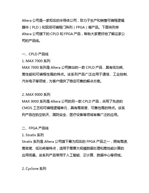
Altera公司是一家知名的半导体公司,致力于生产和销售可编程逻辑器件(PLD)和现场可编程门阵列(FPGA)等产品。
下面将列举Altera公司旗下的CPLD和FPGA产品,帮助大家更好地了解这家公司的产品线。
一、CPLD产品线1. MAX 7000系列MAX 7000系列是Altera公司推出的一款CPLD产品,具有低功耗、高性能和可编程性强的特点。
该系列产品广泛应用于通信、工业控制、汽车电子等领域,为客户提供了稳定可靠的解决方案。
2. MAX 9000系列MAX 9000系列是Altera公司的另一款CPLD产品,采用了先进的CMOS工艺和可编程逻辑单元,具有高密度、可靠性高的特点。
该系列产品在航空航天、国防安全、医疗设备等领域有着广泛的应用。
二、FPGA产品线1. Stratix系列Stratix系列是Altera公司旗下最为知名的FPGA产品之一,拥有高速、高密度、低功耗等特点,适用于需要大规模数据处理和高性能计算的应用场景。
该系列产品常用于人工智能、云计算、数据中心等领域。
2. Cyclone系列Cyclone系列是Altera公司针对中小规模应用市场推出的FPGA产品,具有低成本、低功耗、高性能等特点。
该系列产品在嵌入式系统、工业自动化、网络通信等领域有着广泛的应用。
3. Arria系列Arria系列是Altera公司旗下的高性能FPGA产品,具有高速、低功耗、灵活性强等特点,适用于需要高性能和灵活性的应用场景。
该系列产品在无线通信、高性能计算、高清视频等领域有着广泛的应用。
通过以上列举,我们可以看到Altera公司在CPLD和FPGA领域拥有丰富的产品线,为不同领域的客户提供了多样化的解决方案。
期待Altera在未来能够持续推出更多高性能、低功耗的PLD和FPGA产品,满足客户不断增长的需求。
Altera公司作为半导体行业的领军企业,一直以来致力于为全球各行业提供高性能、低功耗的可编程逻辑器件(PLD)和现场可编程门阵列(FPGA)产品。
EP4CGX15BF14C8N© 2011 Altera Corporation. All rights reserved. ALTERA, ARRIA, CYCLONE, HARDCOPY, MAX, MEGACORE, NIOS, QUARTUS and STRATIX words and logos are trademarks of Altera Corporation and registered in the U.S. Patent and Trademark Office and in other countries. All other words and logos identified astrademarks or service marks are the property of their respective holders as described at /common/legal.html . Altera warrants performance of itssemiconductor products to current specifications in accordance with Altera's standard warranty, but reserves the right to make changes to any products andservices at any time without notice. Altera assumes no responsibility or liability arising out of the application or use of any information, product, or servicedescribed herein except as expressly agreed to in writing by Altera. Altera customers are advised to obtain the latest version of device specifications before relying on any published information and before placing orders for products or services.Cyclone IV Device Handbook,Volume 1November 2011SubscribeISO 9001:2008 Registered 1.Cyclone IV FPGA Device FamilyOverviewAltera’s new Cyclone ®IV FPGA device family extends the Cyclone FPGA series leadership in providing the market’s lowest-cost, lowest-power FPGAs, now with a transceiver variant. Cyclone IV devices are targeted to high-volume, cost-sensitive applications, enabling system designers to meet increasing bandwidth requirements while lowering costs.Built on an optimized low-power process, the Cyclone IV device family offers the following two variants:■Cyclone IV E—lowest power, high functionality with the lowest cost ■Cyclone IV GX—lowest power and lowest cost FPGAs with 3.125Gbps transceivers 1Cyclone IV E devices are offered in core voltage of 1.0V and 1.2V .f For more information, refer to the Power Requirements for Cyclone IV Deviceschapter.Providing power and cost savings without sacrificing performance, along with a low-cost integrated transceiver option, Cyclone IV devices are ideal for low-cost, small-form-factor applications in the wireless, wireline, broadcast, industrial, consumer, and communications industries.Cyclone IV Device Family FeaturesThe Cyclone IV device family offers the following features:■Low-cost, low-power FPGA fabric:■6K to 150K logic elements■Up to 6.3Mb of embedded memory■Up to 360 18 × 18 multipliers for DSP processing intensive applications ■Protocol bridging applications for under 1.5W total power1–2Chapter 1:Cyclone IV FPGA Device Family OverviewCyclone IV Device Family FeaturesCyclone IV Device Handbook,November 2011Altera CorporationVolume 1■Cyclone IV GX devices offer up to eight high-speed transceivers that provide:■Data rates up to 3.125 Gbps ■8B/10B encoder/decoder■8-bit or 10-bit physical media attachment (PMA) to physical coding sublayer (PCS) interface■Byte serializer/deserializer (SERDES)■Word aligner ■Rate matching FIFO■TX bit slipper for Common Public Radio Interface (CPRI)■Electrical idle■Dynamic channel reconfiguration allowing you to change data rates and protocols on-the-fly■Static equalization and pre-emphasis for superior signal integrity ■150 mW per channel power consumption■Flexible clocking structure to support multiple protocols in a single transceiver block■Cyclone IV GX devices offer dedicated hard IP for PCI Express (PIPE) (PCIe) Gen 1:■×1, ×2, and ×4 lane configurations ■End-point and root-port configurations ■Up to 256-byte payload ■One virtual channel ■ 2 KB retry buffer ■4 KB receiver (Rx) buffer■Cyclone IV GX devices offer a wide range of protocol support:■PCIe (PIPE) Gen 1 ×1, ×2, and ×4 (2.5 Gbps)■Gigabit Ethernet (1.25 Gbps)■CPRI (up to 3.072Gbps)■XAUI (3.125 Gbps)■Triple rate serial digital interface (SDI) (up to 2.97Gbps)■Serial RapidIO (3.125 Gbps)■Basic mode (up to 3.125 Gbps)■V-by-One (up to 3.0Gbps)■DisplayPort (2.7Gbps)■Serial Advanced Technology Attachment (SATA) (up to 3.0Gbps)■OBSAI (up to 3.072Gbps)Chapter 1:Cyclone IV FPGA Device Family Overview 1–3Device ResourcesNovember 2011Altera CorporationCyclone IV Device Handbook,Volume 1■Up to 532 user I/Os■LVDS interfaces up to 840Mbps transmitter (Tx), 875Mbps Rx ■Support for DDR2 SDRAM interfaces up to 200MHz ■Support for QDRII SRAM and DDR SDRAM up to 167MHz■Up to eight phase-locked loops (PLLs) per device ■Offered in commercial and industrial temperature gradesDevice ResourcesTable 1–1 lists Cyclone IV E device resources.Table 1–1.Resources for the Cyclone IV E Device FamilyResources E P 4C E 6E P 4C E 10E P 4C E 15E P 4C E 22E P 4C E 30E P 4C E 40E P 4C E 55E P 4C E 75E P 4C E 115Logic elements (LEs)6,27210,32015,40822,32028,84839,60055,85675,408114,480Embedded memory (Kbits)2704145045945941,1342,3402,7453,888Embedded 18 × 18 multipliers1523566666116154200266General-purpose PLLs 224444444Global Clock Networks 101020202020202020User I/O Banks888888888Maximum user I/O (1)179179343153532532374426528Note to Table 1–1:(1)The user I/Os count from pin-out files includes all general purpose I/O, dedicated clock pins, and dual purpose configuration pins. Transceiverpins and dedicated configuration pins are not included in the pin count.1–4Chapter 1:Cyclone IV FPGA Device Family OverviewDevice ResourcesCyclone IV Device Handbook,November 2011Altera CorporationVolume 1Table 1–2 lists Cyclone IV GX device resources.Table 1–2.Resources for the Cyclone IV GX Device FamilyResourcesE P 4C G X 15E P 4C G X 22E P 4C G X 30(1)E P 4C G X 30(2)E P 4C G X 50(3)E P 4C G X 75(3)E P 4C G X 110(3)E P 4C G X 150(3)Logic elements (LEs)14,40021,28029,44029,44049,88873,920109,424149,760Embedded memory (Kbits)5407561,0801,0802,5024,1585,4906,480Embedded 18 × 18 multipliers 0408080140198280360General purpose PLLs 122 4 (4) 4 (4) 4 (4) 4 (4) 4 (4)Multipurpose PLLs 2 (5) 2 (5) 2 (5) 2 (5) 4 (5) 4 (5) 4 (5) 4 (5)Global clock networks 2020203030303030High-speed transceivers (6)24448888Transceiver maximum data rate (Gbps)2.5 2.5 2.53.125 3.125 3.125 3.125 3.125PCIe (PIPE) hard IP blocks11111111User I/O banks 9 (7)9 (7)9 (7)11 (8)11 (8)11 (8)11 (8)11 (8)Maximum user I/O (9)72150150290310310475475Notes to Table 1–2:(1)Applicable for the F169 and F324 packages.(2)Applicable for the F484 package.(3)Only two multipurpose PLLs for F484 package.(4)Two of the general purpose PLLs are able to support transceiver clocking. For more information, refer to the Clock Networks and PLLs inCyclone IV Devices chapter.(5)You can use the multipurpose PLLs for general purpose clocking when they are not used to clock the transceivers. For more information, referto the Clock Networks and PLLs in Cyclone IV Devices chapter.(6)If PCIe 1, you can use the remaining transceivers in a quad for other protocols at the same or different data rates.(7)Including one configuration I/O bank and two dedicated clock input I/O banks for HSSI reference clock input.(8)Including one configuration I/O bank and four dedicated clock input I/O banks for HSSI reference clock input.(9)The user I/Os count from pin-out files includes all general purpose I/O, dedicated clock pins, and dual purpose configuration pins. Transceiverpins and dedicated configuration pins are not included in the pin count.Chapter 1:Cyclone IV FPGA Device Family Overview 1–7Cyclone IV Device Family Speed GradesNovember 2011Altera CorporationCyclone IV Device Handbook,Volume 1Cyclone IV Device Family Speed GradesTable 1–5 lists the Cyclone IV GX devices speed grades.Table 1–6 lists the Cyclone IV E devices speed grades.Table 1–5.Speed Grades for the Cyclone IV GX Device FamilyDevice N148F169F324F484F672F896EP4CGX15C7, C8, I7C6, C7, C8, I7————EP4CGX22—C6, C7, C8, I7C6, C7, C8, I7———EP4CGX30—C6, C7, C8, I7C6, C7, C8, I7C6, C7, C8, I7——EP4CGX50———C6, C7, C8, I7C6, C7, C8, I7—EP4CGX75———C6, C7, C8, I7C6, C7, C8, I7—EP4CGX110———C7, C8, I7C7, C8, I7C7, C8, I7EP4CGX150———C7, C8, I7C7, C8, I7C7, C8, I7Table 1–6.Speed Grades for the Cyclone IV E Device Family (1),(2)Device E144M164U256F256U484F484F780EP4CE6C8L, C9L, I8L C6, C7, C8, I7, A7—I7NC8L, C9L, I8L C6, C7, C8, I7, A7———EP4CE10C8L, C9L, I8L C6, C7, C8, I7, A7—I7N C8L, C9L, I8L C6, C7, C8, I7, A7———EP4CE15C8L, C9L, I8L C6, C7, C8, I7I7N I7N C8L, C9L, I8L C6, C7, C8, I7, A7—C8L, C9L, I8L C6, C7, C8, I7, A7—EP4CE22C8L, C9L, I8L C6, C7, C8, I7, A7—I7N C8L, C9L, I8L C6, C7, C8, I7, A7———EP4CE30—————C8L, C9L, I8LC6, C7, C8,I7, A7C8L, C9L, I8LC6, C7, C8, I7EP4CE40————I7N C8L, C9L, I8LC6, C7, C8,I7, A7C8L, C9L, I8LC6, C7, C8, I7EP4CE55————I7N C8L, C9L, I8L C6, C7, C8, I7C8L, C9L, I8L C6, C7, C8, I7EP4CE75————I7N C8L, C9L, I8L C6, C7, C8, I7C8L, C9L, I8L C6, C7, C8, I7EP4CE115—————C8L, C9L, I8L C7, C8, I7C8L, C9L, I8L C7, C8, I7Notes to Table 1–6:(1)C8L, C9L, and I8L speed grades are applicable for the 1.0-V core voltage.(2)C6, C7, C8, I7, and A7 speed grades are applicable for the 1.2-V core voltage.1–8Chapter 1:Cyclone IV FPGA Device Family OverviewCyclone IV Device Family ArchitectureCyclone IV Device Family ArchitectureThis section describes Cyclone IV device architecture and contains the followingtopics:■“FPGA Core Fabric”■“I/O Features”■“Clock Management”■“External Memory Interfaces”■“Configuration”■“High-Speed Transceivers (Cyclone IV GX Devices Only)”■“Hard IP for PCI Express (Cyclone IV GX Devices Only)”FPGA Core FabricCyclone IV devices leverage the same core fabric as the very successful Cyclone seriesdevices. The fabric consists of LEs, made of 4-input look up tables (LUTs), memoryblocks, and multipliers.Each Cyclone IV device M9K memory block provides 9 Kbits of embedded SRAMmemory. You can configure the M9K blocks as single port, simple dual port, or truedual port RAM, as well as FIFO buffers or ROM. They can also be configured toimplement any of the data widths in Table1–7.Table1–7.M9K Block Data Widths for Cyclone IV Device FamilyMode Data Width ConfigurationsSingle port or simple dual port ×1, ×2, ×4, ×8/9, ×16/18, and ×32/36True dual port ×1, ×2, ×4, ×8/9, and ×16/18The multiplier architecture in Cyclone IV devices is the same as in the existingCyclone series devices. The embedded multiplier blocks can implement an 18 × 18 ortwo 9 × 9 multipliers in a single block. Altera offers a complete suite of DSP IPincluding finite impulse response (FIR), fast Fourier transform (FFT), and numericallycontrolled oscillator (NCO) functions for use with the multiplier blocks. TheQuartus®II design software’s DSP Builder tool integrates MathWorks Simulink andMATLAB design environments for a streamlined DSP design flow.f For more information, refer to the Logic Elements and Logic Array Blocks in Cyclone IVDevices, Memory Blocks in Cyclone IV Devices, and Embedded Multipliers in Cyclone IVDevices chapters.Cyclone IV Device Handbook,November 2011Altera Corporation Volume 1Chapter 1:Cyclone IV FPGA Device Family Overview 1–9Cyclone IV Device Family ArchitectureNovember 2011Altera CorporationCyclone IV Device Handbook,Volume 1I/O FeaturesCyclone IV device I/O supports programmable bus hold, programmable pull-up resistors, programmable delay, programmable drive strength, programmableslew-rate control to optimize signal integrity, and hot socketing. Cyclone IV devices support calibrated on-chip series termination (Rs OCT) or driver impedance matching (Rs) for single-ended I/O standards. In Cyclone IV GX devices, the high-speedtransceiver I/Os are located on the left side of the device. The top, bottom, and right sides can implement general-purpose user I/Os.Table 1–8 lists the I/O standards that Cyclone IV devices support.The LVDS SERDES is implemented in the core of the device using logic elements.f For more information, refer to the I/O Features in Cyclone IV Devices chapter.Clock ManagementCyclone IV devices include up to 30 global clock (GCLK) networks and up to eight PLLs with five outputs per PLL to provide robust clock management and synthesis. You can dynamically reconfigure Cyclone IV device PLLs in user mode to change the clock frequency or phase.Cyclone IV GX devices support two types of PLLs: multipurpose PLLs and general-purpose PLLs:■Use multipurpose PLLs for clocking the transceiver blocks. You can also use them for general-purpose clocking when they are not used for transceiver clocking.■Use general purpose PLLs for general-purpose applications in the fabric andperiphery, such as external memory interfaces. Some of the general purpose PLLs can support transceiver clocking.f For more information, refer to the Clock Networks and PLLs in Cyclone IV Deviceschapter.External Memory InterfacesCyclone IV devices support SDR, DDR, DDR2 SDRAM, and QDRII SRAM interfaces on the top, bottom, and right sides of the device. Cyclone IV E devices also support these interfaces on the left side of the device. Interfaces may span two or more sides of the device to allow more flexible board design. The Altera ® DDR SDRAM memory interface solution consists of a PHY interface and a memory controller. Altera supplies the PHY IP and you can use it in conjunction with your own custom memorycontroller or an Altera-provided memory controller. Cyclone IV devices support the use of error correction coding (ECC) bits on DDR and DDR2 SDRAM interfaces.Table 1–8.I/O Standards Support for the Cyclone IV Device FamilyTypeI/O StandardSingle-Ended I/O LVTTL, LVCMOS, SSTL, HSTL, PCI, and PCI-XDifferential I/OSSTL, HSTL, LVPECL, BLVDS, LVDS, mini-LVDS, RSDS, and PPDSCyclone IV Device Family Architecturef For more information, refer to the External Memory Interfaces in Cyclone IV Deviceschapter.ConfigurationCyclone IV devices use SRAM cells to store configuration data. Configuration data isdownloaded to the Cyclone IV device each time the device powers up. Low-costconfiguration options include the Altera EPCS family serial flash devices andcommodity parallel flash configuration options. These options provide the flexibilityfor general-purpose applications and the ability to meet specific configuration andwake-up time requirements of the applications.Table1–9 lists which configuration schemes are supported by Cyclone IV devices.Table1–9.Configuration Schemes for Cyclone IV Device FamilyDevices Supported Configuration SchemeCyclone IV GX AS, PS, JTAG, and FPP (1)Cyclone IV E AS, AP, PS, FPP, and JTAGNote to Table1–9:(1)The FPP configuration scheme is only supported by the EP4CGX30F484 and EP4CGX50/75/110/150 devices.IEEE 1149.6 (AC JTAG) is supported on all transceiver I/O pins. All other pinssupport IEEE 1149.1 (JTAG) for boundary scan testing.f For more information, refer to the JTAG Boundary-Scan Testing for Cyclone IV Deviceschapter.For Cyclone IV GX devices to meet the PCIe 100ms wake-up time requirement, youmust use passive serial (PS) configuration mode for the EP4CGX15/22/30 devicesand use fast passive parallel (FPP) configuration mode for the EP4CGX30F484 andEP4CGX50/75/110/150 devices.f For more information, refer to the Configuration and Remote System Upgrades inCyclone IV Devices chapter.The cyclical redundancy check (CRC) error detection feature during user mode issupported in all Cyclone IV GX devices. For Cyclone IV E devices, this feature is onlysupported for the devices with the core voltage of 1.2V.f For more information about CRC error detection, refer to the SEU Mitigation inCyclone IV Devices chapter.High-Speed Transceivers (Cyclone IV GX Devices Only)Cyclone IV GX devices contain up to eight full duplex high-speed transceivers thatcan operate independently. These blocks support multiple industry-standardcommunication protocols, as well as Basic mode, which you can use to implementyour own proprietary protocols. Each transceiver channel has its own pre-emphasisand equalization circuitry, which you can set at compile time to optimize signalintegrity and reduce bit error rates. Transceiver blocks also support dynamicreconfiguration, allowing you to change data rates and protocols on-the-fly.Cyclone IV Device Handbook,November 2011Altera Corporation Volume 1Cyclone IV Device Family ArchitectureFigure1–1 shows the structure of the Cyclone IV GX transceiver.Figure1–1.Transceiver Channel for the Cyclone IV GX Devicef For more information, refer to the Cyclone IV Transceivers Architecture chapter.Hard IP for PCI Express (Cyclone IV GX Devices Only)Cyclone IV GX devices incorporate a single hard IP block for ×1, ×2, or ×4 PCIe(PIPE)in each device. This hard IP block is a complete PCIe(PIPE) protocol solution thatimplements the PHY-MAC layer, Data Link Layer, and Transaction Layerfunctionality. The hard IP for the PCIe (PIPE) block supports root-port and end-pointconfigurations. This pre-verified hard IP block reduces risk, design time, timingclosure, and verification. You can configure the block with the Quartus II software’sPCI Express Compiler, which guides you through the process step by step.f For more information, refer to the PCI Express Compiler User Guide.November 2011Altera Corporation Cyclone IV Device Handbook,Volume 1Reference and Ordering InformationCyclone IV Device Handbook,November 2011Altera CorporationVolume 1Reference and Ordering InformationFigure 1–2 shows the ordering codes for Cyclone IV GX devices.Figure 1–3 shows the ordering codes for Cyclone IV E devices.Figure 1–2.Packaging Ordering Information for the Cyclone IVGX DeviceFigure 1–3.Packaging Ordering Information for the Cyclone IVE DeviceDocument Revision HistoryNovember 2011Altera CorporationCyclone IV Device Handbook,Volume 1Document Revision HistoryTable 1–10 lists the revision history for this chapter.Table 1–10.Document Revision HistoryDateVersion ChangesNovember 20111.5■Updated “Cyclone IV Device Family Features” section.■Updated Figure 1–2 and Figure 1–3.December 2010 1.4■Updated for the Quartus II software version 10.1 release.■Added Cyclone IV E new device package information.■Updated Table 1–1, Table 1–2, Table 1–3, Table 1–5, and Table 1–6.■Updated Figure 1–3.■Minor text edits.July 2010 1.3Updated Table 1–2 to include F484 package information.March 20101.2■Updated Table 1–3 and Table 1–6.■Updated Figure 1–3.■Minor text edits.February 2010 1.1■Added Cyclone IV E devices in Table 1–1, Table 1–3, and Table 1–6 for the Quartus II software version 9.1 SP1 release.■Added the “Cyclone IV Device Family Speed Grades” and “Configuration” sections.■Added Figure 1–3 to include Cyclone IV E Device Packaging Ordering Information.■Updated Table 1–2, Table 1–4, and Table 1–5 for Cyclone IV GX devices.■Minor text edits.November 2009 1.0Initial release.Document Revision History Cyclone IV Device Handbook,November 2011Altera Corporation Volume 1EP4CGX15BF14C8N。
Altera FPGA下载配置很多兄弟对于CPLD下JTAG的下载很熟悉了,可转到FPGA来的时候,多多少少有些迷惑,怎么出现配置芯片了,为什么要用不同的下载电缆,不同的下载模式?我就自己知道的一点东西谈一些个人的见解,并发一些资料.1.FPGA器件有三类配置下载方式:主动配置方式(AS)和被动配置方式(PS)和最常用的(JTAG)配置方式。
AS由FPGA器件引导配置操作过程,它控制着外部存储器和初始化过程,EPCS系列.如EPCS1,EPCS4配置器件专供AS模式,目前只支持Cyclone系列。
使用Altera串行配置器件来完成。
Cyclone器件处于主动地位,配置器件处于从属地位。
配置数据通过DATA0引脚送入FPGA。
配置数据被同步在DCLK输入上,1个时钟周期传送1位数据。
(见附图) PS则由外部计算机或控制器控制配置过程。
通过加强型配置器件(EPC16,EPC8,EPC4)等配置器件来完成,在PS配置器件,配置数据从外部储存部件,通过DATA0引脚送入FPGA。
配置数据在DCLK上升沿锁存,1个时钟周期传送1位数据。
(见附图)JTAG接口是一个业界标准,主要用于芯片测试等功能,使用IEEE Std 1149.1联合边界扫描接口引脚,支持JAM STAPL标准,可以使用Altera下载电缆或主控器来完成。
FPGA在正常工作时,它的配置数据存储在SRAM中,加电时须重新下载。
在实验系统中,通常用计算机或控制器进行调试,因此可以使用PS。
在实用系统中,多数情况下必须由FPGA主动引导配置操作过程,这时FPGA将主动从外围专用存储芯片中获得配置数据,而此芯片中fpga配置信息是用普通编程器将设计所得的pof格式的文件烧录进去。
专用配置器件:epc型号的存储器常用配置器件:epc2,epc1,epc4,epc8,epc1441(现在好象已经被逐步淘汰了)等对于cyclone cycloneII系列器件,ALTERA还提供了针对AS方式的配置器件,EPCS系列.如EPCS1,EPCS4配置器件也是串行配置的.注意,他们只适用于cyclone系列.除了AS和PS等单BIT配置外,现在的一些器件已经支持PPS,FPS等一些并行配置方式,提升了配置速度。
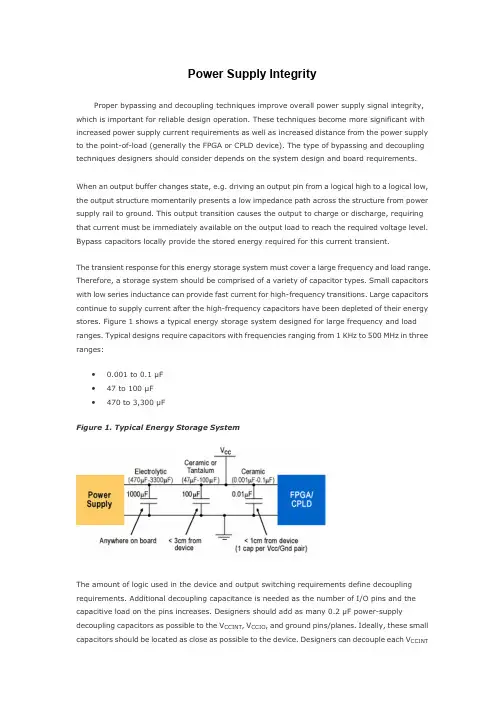
Power Supply IntegrityProper bypassing and decoupling techniques improve overall power supply signal integrity, which is important for reliable design operation. These techniques become more significant with increased power supply current requirements as well as increased distance from the power supply to the point-of-load (generally the FPGA or CPLD device). The type of bypassing and decoupling techniques designers should consider depends on the system design and board requirements.When an output buffer changes state, e.g. driving an output pin from a logical high to a logical low, the output structure momentarily presents a low impedance path across the structure from power supply rail to ground. This output transition causes the output to charge or discharge, requiring that current must be immediately available on the output load to reach the required voltage level. Bypass capacitors locally provide the stored energy required for this current transient.The transient response for this energy storage system must cover a large frequency and load range. Therefore, a storage system should be comprised of a variety of capacitor types. Small capacitors with low series inductance can provide fast current for high-frequency transitions. Large capacitors continue to supply current after the high-frequency capacitors have been depleted of their energy stores. Figure 1 shows a typical energy storage system designed for large frequency and load ranges. Typical designs require capacitors with frequencies ranging from 1 KHz to 500 MHz in three ranges:•0.001 to 0.1 µF•47 to 100 µF•470 to 3,300 µFFigure 1. Typical Energy Storage SystemThe amount of logic used in the device and output switching requirements define decoupling requirements. Additional decoupling capacitance is needed as the number of I/O pins and the capacitive load on the pins increases. Designers should add as many 0.2 µF power-supply decoupling capacitors as possible to the V CCINT, V CCIO, and ground pins/planes. Ideally, these small capacitors should be located as close as possible to the device. Designers can decouple each V CCINTor V CCIO and ground pin pair with a 0.2-µF capacitor. If a design uses high-density packages such as ball grid array (BGA) packages, it may be difficult to use one decoupling capacitor per V CCINT / V CCIO and ground pin pair. In such cases, designers make every effort to use as many decoupling capacitors as allowed by the layout. Decoupling capacitors should have a good frequency response, such as monolithic-ceramic capacitors.Capacitor Choice & PlacementProper placement and location are very important for high-frequency capacitors (0.001 to 0.1 µF low inductance ceramic chip). Designers should minimize trace lengths when possible to reduce the inductance in the path from capacitor terminals to the device power pins. This includes paths that go through a solid ground or power plane (V CCINT or V CCIO) where the inductance of one inch of solid copper plane is about 1 nH. Bypass capacitor vias should route directly to ground, V CCINT, or V CCIO planes. Other capacitor types (47 to 100 µF medium-frequency and 470 to 3,300 µFlow-frequency capacitors) are referred to as “bulk” capacitance and can be mounted anywhere on the board. Designers should, however, locate bulk capacitance as close to the device as possible. Place V CCINT or V CCIO high-frequency bypass capacitors within one centimeter of the associatedV CCINT or V CCIO pin on the PCB. V CCINT or V CCIO medium-frequency bypass capacitors should be placed within 3 cm of V CCINT or V CCIO pins.V CCINT Bypass CapacitanceIn the case of Stratix® II, individual logic array structures within different architectural features conduct very small currents (picoamps or less) for very short durations (< 50 ps). Although these currents are small, when added up across the entire device they can add up to several amperes of current. Considering that these minute current transitions can occur hundreds of millions of times per second, along with the existence of millions of individual switches carrying out these transitions, bypass capacitor calculation is based on an average energy storage requirement. High-frequency capacitor values can be approximated with:logic array power = equivalent switched logic array capacitance × V CCINT2 × clock frequencyorequivalent switched logic array capacitance = (logic array power) / (V CCINT2 × clock frequency)The equivalent switched logic array capacitance is the equivalent switched capacitance of the entire Stratix II logic array powered by V CCINT. In order to reduce power noise, the V CCINT power supply bypass capacitor must be significantly larger than the equivalent switched logic array capacitance. High-frequency bypass capacitors should be 25 to 100 times larger than the equivalent switched logic array capacitance. A factor of 50 will result in a 2 percent variation ofV CCINT.High-frequency bypass capacitance = <25 to 100> × equivalent switched logic array capacitanceEvery V CCINT and ground pin pair should have a high-frequency bypass capacitor. To determine the optimum size of each high-frequency bypass capacitor, divide the total high-frequency bypass capacitance by the number of V CCINT pins on the device, and round up to the next commonly available value. Therefore, the minimum size of each high-frequency V CCINT capacitor is:Capacitor size = (<25 to 100> × equivalent switched logic array capacitance) / number of V CCINT pins= (<25 to 100> / number of V CCINT pins) × logic array power / (V CCINT2 ×clock-frequency)Consider the following example:•Device V CCINT power = 5 W•V CCINT = 1.2 V•System clock frequency = 150 MHz•High-frequency bypass capacitor multiplier = 50•Number of device V CCINT pins = 36Capacitor size = (50 / 36 ) x 5W / (1.2V2 x 150MHz)= 3.215E-08= 0.03215E-06The capacitor size should be at least 0.032 µF. Given this example, the designer should select individual high-frequency capacitors at least this large.The medium-frequency capacitors should be tantalum capacitors from 47 µF to 100 µF. If tantalum is not available, low-inductance aluminum electrolytic capacitors can be used. Stratix II devices require at least four medium-frequency capacitors mounted within 3 cm of the device. In addition, at least one low-frequency capacitor (470 µF to 3300 µF) is required on the PCB.V CCIO Bypass CapacitanceSimilar to V CCINT considerations, V CCIO bypass requirements are also based on an average energy storage requirement. The loads driven by the FPGA or CPLD device determine the size of the equivalent switched capacitance. Since different I/O banks can operate at different voltages and different switching frequencies, designers should consider bypassing networks individually, using the equations below to determine high-frequency capacitor requirements.In order to reduce the amount of V CCIO noise, bypass capacitance must be significantly greater than the total output load capacitance. High-frequency bypass capacitance should be 25 to 100 times the total load capacitance. Every V CCIO and ground pair should have a high-frequency bypass capacitor to provide immediate current needs when the device has a large current draw. The following equations determine the optimum size of each capacitor:equivalent switched I/O capacitance (per V CCIO) = number of loads × average load peroutput signalhigh-frequency I/O capacitance =<25 to 100> × equivalent switched I/Ocapacitanceindividual capacitor size = high-frequency I/O capacitance / numberof VCCIO pins in the bank= (<25 to 100> / number of VCCIO pins) ×number of loads × average load per outputsignalConsider the following example:•Number of loads = 40 signals•Average load value = 10pF•High-frequency bypass capacitor multiplier = 50•Number of device V CCIO pins = 5Capacitor size = (50 / 5) * 40 * 10pF= 4.0E-09= 0.004E-06The capacitor size should be 0.004 µF. Given this example, the designer should select individual high-frequency capacitors at least this large. The next larger available capacitor size should be chosen (0.047 µF or 0.01 µF).Medium-frequency capacitors should be tantalum capacitors from 47 µF to 100 µF. Onemiddle-frequency capacitor is required for every two V CCIO banks. If tantalum capacitors are not available, low-inductance aluminum electrolytic capacitors can be used. These capacitors should be located within 3 cm of the V CCIO pin connections. Lastly, at least one low-frequency capacitor (470 µF to 3,300 µF) is required on the PCB for each V CCIO voltage level.。
1I nformation furnished by Linear Technology Corporation is believed to be accurate and reliable.However, no responsibility is assumed for its use. Linear Technology Corporation makes no represen-tation that the interconnection of its circuits as described herein will not infringe on existing patent rights.22ms/DIV DSOL43 F03Figure 3. Up/Down Coincident Rail Tracking of the LTC37080.5V/DIV0.5V/DIV2ms/DIV DSOL43 F04Figure 4. Up/Down Ratiometric Rail Tracking of the LTC370834567891011Design Solutions 43dsol43faOutput CapacitanceSelect capacitors with low ESR to minimize the output voltage ripple. Low ESR capacitors include the Sanyo Poscap, Panasonic Specialty Polymer, Kemet AO-Cap,Kemet polymer tantalums (T520), as well as a variety of low ESR solid tantalums. Pay careful attention to the voltage derating. Multilayer ceramic capacitors can also be used, but they have very low ESR which makes loop compensation more challenging. Refer to Linear Technol-ogy Application Note 76 for more details.Input CapacitanceThe input capacitance must supply the pulsed current that flows through the top FET. Select C IN with a ripple current rating that meets or exceeds the maximum expected ripple current. The capacitance value must also be high enough for adequate circuit stability.Sanyo OS-CONs or similar parts are a good choice due to their high RMS current ratings and their high capacitance.However, they have high series inductance (ESL). To minimize the ESL, a ceramic capacitor should be paral-leled with the OS-CON and placed next to the top and bottom FETs.Aluminum electrolytics are inexpensive, but their RMS current ratings are low relative to OS-CONs and their ESL is also high. Sometimes, a carefully selected parallel combination of aluminum electrolytics and high grade ceramics can be used where the ceramics handle the ripple current and the aluminum electrolytics provide the bulk capacitance for stability.MOSFETsFor the controllers, external MOSFETs are required. The bottom FET needs to have a low R DS(ON) to minimize conduction losses. The top FET needs to have a low gate charge (Q G ) to minimize transition losses, and if the duty cycle is high, a low value of R DS(ON) as well. Make sure the current rating of the MOSFET is not exceeded. Contact the MOSFET vendor for more details. MOSFET vendors in-clude Vishay Siliconix, Renesas, International Rectifier,and Fairchild.SWITCHING FREQUENCYThe controllers shown in Table 1 operate at various frequencies. The LTC3407 operates at a fixed frequency of 1.5MHz. The switching frequency on the other parts can be set within a range by a voltage or a resistor. For the fixed on-time parts, the switching frequency is determined by the output voltage and programmed on-time. Refer to the individual data sheets for more details.LOOP COMPENSATIONAll of the controllers shown in Table 1 use current mode control. In the simplest model of a current mode buck regulator, the output inductor is considered to be a current source controlled by the output voltage of the error ampli-fier. This reduces the output power stage to a first order system with the output capacitance forming the dominant pole. Both the value of C OUT and its ESR are critical in designing a stable loop in addition to the compensation components and the feedback divider. Refer to Linear Technology’s Application Note 76 for more details.12Design Solutions 43dsol43fa© Linear Technology Corporation1630 McCarthy Blvd., Milpitas, CA 95035-7417(408) 432-1900 ● FAX: (408) 434-0507 ● LAYOUTBoard layout is a very critical step in designing a switch mode step-down regulator. A poor layout can affect stabil-ity, regulation and reliability. Refer to the individual data sheets for specific guidelines as well as the demo board gerber files. Here are several points to keep in mind when addressing layout issues for controllers:•Devote entire layers or planes for the ground, all output voltages and the input voltage. Liberally spread the copper for these signals.•Make all of the high current connections as wide and short as possible.•Place a ground plane underneath the controller.•Keep the signal ground (SGND) and power grounds (PGND) separate, and tie SGND to PGND at one loca-tion.•The loop area formed by the top FET, bottom FET and ceramic input capacitor should be as small as possible.•Keep the high dV/dt traces away from the control signals.•If necessary, shield the high dV/dt traces on one layer from the control signals on another with the GND plane,V IN plane or V OUT plane.•Use Kelvin current sensing for the current sense lines (if applicable).•Allow sufficient copper for heat-spreading.。