KDM2401/2461硬件安装手册
- 格式:pdf
- 大小:1.48 MB
- 文档页数:25

传输设备硬件安装操作指导1. 概述本文档旨在提供有关传输设备硬件安装的操作指导。
在进行任何硬件安装操作之前,请确保您已经阅读并理解了设备的安全说明和操作手册。
2. 硬件准备在开始安装传输设备之前,您需要根据设备的规格和要求准备以下硬件:2.1 主机设备•一台适用于传输设备的电脑或服务器。
•必要的接口和插槽,如PCIe插槽或USB接口。
2.2 传输设备•传输设备主体。
•配套的电源适配器。
•所需的数据线缆,如SATA数据线缆或USB线缆。
•其他必要的附件,如安装支架或固定螺丝。
3. 安装步骤请按照以下步骤操作以完成传输设备的安装:3.1 准备工作在开始安装之前,请先关闭主机设备,并断开与电源的连接。
确保您处于一个无尘、无静电的工作环境中,以防止对设备造成静电击穿或其他损坏。
3.2 连接传输设备根据传输设备的接口类型,选择相应的数据线缆,并将其连接到传输设备和主机设备之间的接口上。
确保连接牢固,握紧相关接口的螺丝。
3.3 安装传输设备根据传输设备的安装方式,选择合适的安装支架或固定螺丝,并将传输设备安装到主机设备的相应插槽或位置上。
确保传输设备与主机设备接触良好,并且稳固固定。
3.4 连接电源将传输设备的电源适配器插头连接到设备的电源接口上。
然后,将适配器的另一端插入电源插座。
确保该连接牢固,电源供电正常。
3.5 检查和测试完成安装后,重新连接主机设备的电源,并开机进行检查和测试。
确保传输设备被主机设备正常识别,并且可以在操作系统中被访问和使用。
如果设备无法正常工作,建议检查连接和安装步骤是否正确,并参考设备的相关文档进行故障排除。
4. 安全注意事项在硬件安装过程中,请注意以下安全事项:•确保设备和主机都处于关机状态,并断开与电源的连接。
•使用适当的工具和附件,确保设备的稳固安装。
•小心处理数据线缆和电源适配器,避免扭曲或损坏。
•阅读并理解传输设备的安全说明和操作手册,确保正确操作。
5. 总结本文档提供了传输设备硬件安装的操作指导。
BDCOM2641 路由器硬件安装手册目录目录第1章 BDCOM 2641模块化路由器概述 (1)1.1 标准配置时的外形说明 (1)1.2 路由器系统特性参数 (3)1.3 ROHS说明 (4)第2章安装准备 (5)2.1 路由器使用注意事项 (5)2.2 安全建议 (5)2.3 一般场所要求 (7)2.3.1 场所环境 (7)2.3.2 场所配置预防 (7)2.3.3 机架配置 (7)2.3.4 电源考虑 (8)2.4 安装工具和设备 (8)第3章安装路由器 (9)3.1 路由器机箱安装 (9)3.1.1 安装机箱于桌面 (9)3.1.2 安装机箱于机架 (9)3.2 连接接口 (10)3.2.1 连接监控口 (10)3.2.2 连接快速以太网接口 (12)3.3 网络模块 (13)3.4 安装后检查 (15)第4章路由器维护 (16)4.1 打开机箱 (16)4.2 系统存储器升级 (17)4.2.1 SDRAM安装方法 (17)4.2.2 扩展FLASH (19)4.3 关闭机箱 (19)第5章硬件故障分析 (21)5.1 故障隔离 (21)5.1.1 电源和冷却系统故障 (21)5.1.2 端口、电缆和连接故障 (21)5.2 指示灯说明 (21)第1章BDCOM 2641模块化路由器概述本节主要对BDCOM2641模块化路由器总体方面的特性、参数作了说明和介绍,让读者对BDCOM2641模块化路由器有一个总体的认识。
本公司每款路由器都有直流电源和交流电源两种,BDCOM 2641-DC是使用直流电源的2641路由器。
1.1 标准配置时的外形说明BDCOM 2641模块化路由器标配端口由三个部分组成:一个Console端口,一个AUX端口,两个10/100M以太网口。
详细说明如下表。
表 1-1 标配端口特性表端口名称特点Console端口速率300bps—115200bps,RJ45接口,无指示灯AUX端口 速率1200bps—57600bps,RJ45接口,无指示灯10/100M以太网端口速率10Mbps,100Mbps,2个RJ45接口此外,还有三个接口模块插槽、一个电源插孔,一个电源开关(ON:开;OFF:关)。
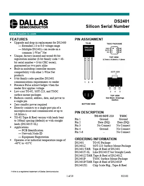
FEATURES§ Upgrade and drop-in replacement for DS2400— Extended 2.8 to 6.0 voltage range — Multiple DS2401s can reside on a common 1-Wire â Net§ Unique, factory-lasered and tested 64-bitregistration number (8-bit family code + 48-bit serial number + 8-bit CRC tester);guaranteed no two parts alike§ Built-in multidrop controller ensures compatibility with other 1-Wire Net products§ 8-bit family code specifies DS2401communications requirements to reader § Presence Pulse acknowledges when the reader first applies voltage§ Low-cost TO-92, SOT-223, and TSOC surface mount packages§ Reduces control, address, data, and power to a single pin§ Zero standby power required§ Directly connects to a single port pin of a microprocessor and communicates at up to 16.3kbits/s§ TO-92 Tape & Reel version with leads bent to 100mil spacing (default) or with straight leads (DS2401T-SL)§ Applications— PCB Identification — Network Node ID— Equipment Registration§ Operates over industrial temperature range of -40°C to +85°CPIN ASSIGNMENTPIN DESCRIPTIONTO-92/SOT-223TSOC Pin 1Ground Ground Pin 2Data (DQ)Data (DQ)Pin 3No Connect No Connect Pin 4Ground No Connect Pin 5-6-No ConnectORDERING INFORMATIONDS2401 TO-92 Package DS2401Z SOT-223 Surface Mount Package DS2401/T&R Tape & Reel of DS2401DS2401T-SL Like DS2401T but Straight Leads DS2401Z/T&R Tape & Reel of DS2401Z DS2401P TSOC Surface Mount Package DS2401P/T&R Tape & Reel of DS2401P DS2401X1 Chip Scale Pkg., Tape & ReelDS2401Silicon Serial NumberTOP VIEWSee Mech. DrawingsSectionTOP VIEW3.7mm x4.0mm x 1.5mmBOTTOM VIEWTO-921 2 31-Wire is a registered trademark of Dallas Semiconductor.TSOC PACKAGEDESCRIPTIONThe DS2401 enhanced Silicon Serial Number is a low-cost, electronic registration number that provides an absolutely unique identity which can be determined with a minimal electronic interface (typically, a single port pin of a microcontroller). The DS2401 consists of a factory-lasered, 64-bit ROM that includes a unique 48-bit serial number, an 8-bit CRC, and an 8-bit Family Code (01h). Data is transferred serially via the 1-Wire protocol that requires only a single data lead and a ground return. Power for reading and writing the device is derived from the data line itself with no need for an external power source. The DS2401 is an upgrade to the DS2400. The DS2401 is fully reverse-compatible with the DS2400 but provides the additional multi-rop capability that enables many devices to reside on a single data line. The familiar TO-92, SOT-223 or TSOC package provides a compact enclosure that allows standard assembly equipment to handle the device easily.OPERATIONThe DS2401’s internal ROM is accessed via a single data line. The 48-bit serial number, 8-bit family code and 8-bit CRC are retrieved using the Dallas 1-Wire protocol. This protocol defines bus transactions in terms of the bus state during specified time slots that are initiated on the falling edge of sync pulses from the bus master. All data is read and written least significant bit first.1-WIRE BUS SYSTEMThe 1-Wire bus is a system which has a single bus master system and one or more slaves. In all instances, the DS2401 is a slave device. The bus master is typically a microcontroller. The discussion of this bus system is broken down into three topics: hardware configuration, transaction sequence, and 1-Wire signaling (signal type and timing). For a more detailed protocol description, refer to Chapter 4 of the Book of DS19xx iButton® Standards.Hardware ConfigurationThe 1-Wire bus has only a single line by definition; it is important that each device on the bus be able to drive it at the appropriate time. To facilitate this, each device attached to the 1-Wire bus must have an open-drain connection or 3-state outputs. The DS2401 is an open-drain part with an internal circuit equivalent to that shown in Figure 2. The bus master can be the same equivalent circuit. If a bidirectional pin is not available, separate output and input pins can be tied together. The bus master requires a pullup resistor at the master end of the bus, with the bus master circuit equivalent to the one shown in Figure 3. The value of the pullup resistor should be approximately 5k W for short line lengths. A multidrop bus consists of a 1-Wire bus with multiple slaves attached. The 1-Wire bus has a maximum data rate of 16.3kbits per second.The idle state for the 1-Wire bus is high. If, for any reason, a transaction needs to be suspended, the bus MUST be left in the idle state if the transaction is to resume. If this does not occur and the bus is left low for more than 120m s, one or more of the devices on the bus may be reset.DS2401 MEMORY MAP Figure 18-Bit CRC Code48-Bit Serial Number8-Bit Family Code (01h) MSB LSB MSB LSB MSB LSBiButton is a registered trademark of Dallas Semiconductor.DS2401 EQUIVALENT CIRCUIT Figure 2BUS MASTER CIRCUIT Figure 3A) Open DrainSee noteTo data connectionof DS2401B) Standard TTLSee noteTo data connectionof DS2401Note:Depending on the 1-Wire communication speed and the bus load characteristics, the optimal pullup resistor (R PU) value will be in the 1.5k W to 5k W range.TRANSACTION SEQUENCEThe sequence for accessing the DS2401 via the 1-Wire port is as follows:§Initialization§ROM Function Command§Read DataINITIALIZATIONAll transactions on the 1-Wire bus begin with an initialization sequence. The initialization sequence consists of a reset pulse transmitted by the bus master followed by a Presence Pulse(s) transmitted by the slave(s).The Presence Pulse lets the bus master know that the DS2401 is on the bus and is ready to operate. For more details, see the 1-Wire Signaling section.ROM FUNCTION COMMANDSOnce the bus master has detected a presence, it can issue one of the four ROM function commands. All ROM function commands are 8 bits long. A list of these commands follows (refer to flowchart in Figure 4):Read ROM [33h] or [0Fh]This command allows the bus master to read the DS2401’s 8-bit family code, unique 48-bit serial number, and 8-bit CRC. This command can only be used if there is a single DS2401 on the bus. If more than one slave is present on the bus, a data collision will occur when all slaves try to transmit at the same time (open drain will produce a wired-AND result). The DS2401 Read ROM function will occur with a command byte of either 33h or 0Fh in order to ensure compatibility with the DS2400, which will only respond to a 0Fh command word with its 64-bit ROM data.Match ROM [55h] / Skip ROM [CCh]The complete 1-Wire protocol for all Dallas Semiconductor iButtons contains a Match ROM and a Skip ROM command. (See the Book of DS19xx iButton Standards.) Since the DS2401 contains only the 64-bit ROM with no additional data fields, the Match ROM and Skip ROM are not applicable and will cause no further activity on the 1-Wire bus if executed. The DS2401 does not interfere with other 1-Wire parts on a multidrop bus that do respond to a Match ROM or Skip ROM (for example, a DS2401 and DS1994 on the same bus).Search ROM [F0h]When a system is initially brought up, the bus master might not know the number of devices on the 1-Wire bus or their 64-bit ROM codes. The search ROM command allows the bus master to use a process of elimination to identify the 64-bit ROM codes of all slave devices on the bus. The ROM search process is the repetition of a simple 3-step routine: read a bit, read the complement of the bit, then write the desired value of that bit. The bus master performs this simple 3-step routine on each bit of the ROM. After one complete pass, the bus master knows the contents of the ROM in one device. The remaining number of devices and their ROM codes may be identified by additional passes. See Chapter 5 of the Book of DS19xx iButton Standards for a comprehensive discussion of a ROM search, including an actual example.1-WIRE SIGNALINGThe DS2401 requires a strict protocol to ensure data integrity. The protocol consists of four types of signaling on one line: reset sequence with Reset Pulse and Presence Pulse, write 0, write 1, and read data. All these signals except Presence Pulse are initiated by the bus master.The initialization sequence required to begin any communication with the DS2401 is shown in Figure 5.A reset pulse followed by a Presence Pulse indicates the DS2401 is ready to send or receive data given the correct ROM command.The bus master transmits (T X) a reset pulse (t RSTL, minimum 480m s). The bus master then releases the line and goes into receive mode (R X). The 1-Wire bus is pulled to a high state via the 5k W pullup resistor. After detecting the rising edge on the data pin, the DS2401 waits (t PDH, 15-60m s) and then transmits the Presence Pulse (t PDL, 60-240m s). The 1-Wire bus requires a pullup resistor range of 1.5k W to 5k W, depending on bus load characteristics.READ/WRITE TIME SLOTSThe definitions of write and read time slots are illustrated in Figure 6. All time slots are initiated by the master driving the data line low. The falling edge of the data line synchronizes the DS2401 to the master by triggering a delay circuit in the DS2401. During write time slots, the delay circuit determines when the DS2401 will sample the data line. For a read data time slot, if a “0” is to be transmitted, the delay circuit determines how long the DS2401 will hold the data line low overriding the “1” generated by the master. If the data bit is a 1, the DS2401 will leave the read data time slot unchanged.ROM FUNCTIONS FLOW CHART Figure 4INITIALIZATION PROCEDURE “RESET AND PRESENCE PULSES” Figure 5480m s £ t RSTL < ¥ *480m s £ t RSTH < ¥ (includes recovery time)15m s £ t PDH < 60m s 60m s £ t PDL < 240m s* In order not to mask interrupt signaling by other devices on the 1-Wire bus, t RSTL + t R should always be less than 960m s.READ/WRITE TIMING DIAGRAM Figure 6Write-One Time Slot60m s £ t SLOT < 120m s 1m s £ t LOW1 < 15m s 1m s £ t REC < ¥RESISTOR MASTERRESISTOR MASTER DS2401READ/WRITE TIMING DIAGRAM (cont’d) Figure 6Write-zero Time Slot60m s £ t LOW0 < t SLOT < 120m s 1m s £ t REC < ¥Read-data Time Slot60m s £ t SLOT < 120m s 1m s £ t LOWR < 15m s 0 £ t RELEASE < 45m s 1m s £ t REC < ¥ t RDV = 15m s t SU < 1m sCRC GENERATIONTo validate the data transmitted from the DS2401, the bus master may generate a CRC value from the data as it is received. This generated value is compared to the value stored in the last 8 bits of the DS2401. If the two CRC values match, the transmission is error-free.The equivalent polynomial function of this CRC is: CRC = x 8 + x 5 + x 4 + 1. For more details, see the Book of DS19xx iButton Standards .CUSTOM DS2401Customization of a portion of the unique 48-bit serial number by the customer is available. Dallas Semiconductor will register and assign a specific customer ID in the 12 most significant bits of the 48-bit field. The next most significant bits are selectable by the customer as a starting value, and the least significant bits are non-selectable and will be automatically incremented by one. Certain quantities and conditions apply for these custom parts. Contact your Dallas Semiconductor sales representative for more information.RESISTOR MASTER DS2401ABSOLUTE MAXIMUM RATINGS*Voltage on any Pin Relative to Ground -0.5V to +7.0VOperating Temperature Range-40°C to +85°CStorage Temperature Range-55°C to +125°CSoldering Temperature See J-STD-020A Specification*This is a stress rating only and functional operation of the device at these or any other conditions above those indicated in the operation sections of this specification is not implied. Exposure to absolute maximum rating conditions for extended periods of time may affect reliability.DC ELECTRICAL CHARACTERISTICS (-40°C to +85°C; V PUP= 2.8V to 6.0V) PARAMETER SYMBOL MIN TYP MAX UNITS NOTES Logic 1V IH 2.2V CC +0.3V1,6 Logic 0V IL-0.3+0.8V1, 11 Output Logic Low @ 4 mA V OL0.4V1 Output Logic High V OH V PUP 6.0V1,2 Input Load Current I L5m A3 Operating Charge Q OP30nC7,8 CAPACITANCE(t A= +25°C) PARAMETER SYMBOL MIN TYP MAX UNITS NOTES I/O (1-Wire)C IN/OUT800pF9AC ELECTRICAL CHARACTERISTICS (-40°C to +85°C; V PUP= 2.8V to 6.0V) PARAMETER SYMBOL MIN TYP MAX UNITS NOTES Time Slot t SLOT60120m sWrite 1 Low Time t LOW1115m s13 Write 0 Low Time t LOW060120m sRead Data Valid t RDV15m s12 Release Time t RELEASE01545m sRead Data Setup t SU1m s5 Recovery Time t REC1m sReset Time High t RSTH480m s4 Reset Time Low t RSTL480960m s10 Presence Detect High t PDH1560m sPresence Detect Low t PDL60240m sNOTES:1)All voltages are referenced to ground.2)V PUP= external pullup voltage.3)Input load is to ground.4)An additional reset or communication sequence cannot begin until the reset high time has expired.5)Read data setup time refers to the time the host must pull the 1-Wire bus low to read a bit. Data isguaranteed to be valid within 1m s of this falling edge and will remain valid for 14m s minimum (15m s total from falling edge on 1-Wire bus).6)V IH is a function of the external pullup resistor and the V CC supply.7)*********************************.8)At V CC= 5.0V with a 5k W pullup to V CC and a maximum time slot of 120m s.9)Capacitance on the I/O pin could be 800pF when power is first applied. If a 5k W resistor is used topullup the I/O line to V CC, 5m s after power has been applied the parasite capacitance will not affect normal communications.10)The reset low time (t RSTL) should be restricted to a maximum of 960m s, to allow interrupt signaling,otherwise it could mask or conceal interrupt pulses if this device is used in parallel with a DS2404 or DS1994.11)Under certain low voltage conditions, V ILMAX may have to be reduced to as much as 0.5V to alwaysguarantee a Presence Pulse.12)The optimal sampling point for the master is as close as possible to the end time of the t RDV periodwithout exceeding t RDV. For the case of a Read-One Time slot, this maximizes the amount of time for the pullup resistor to recover to a high level. For a Read-Zero Time slot, it ensures that a read will occur before the fastest 1-Wire device(s) releases the line.13)The duration of the low pulse sent by the master should be a minimum of 1µs with a maximum valueas short as possible to allow time for the pullup resistor to recover the line to a high level before the 1-Wire device samples in the case of a Write-One Time or before the master samples in the case of a Read-One Time.。
第1篇一、概述嵌入式控制单元FCU2401是一款高性能、低功耗的嵌入式控制器,适用于工业自动化、智能家居、汽车电子等领域。
本文将详细介绍FCU2401的使用方法,包括硬件连接、软件编程、调试与维护等。
二、硬件连接1. 电源连接将电源线插入FCU2401的电源接口,确保电源电压符合产品规格要求。
FCU2401支持DC12V-24V宽电压输入。
2. 信号输入根据实际需求,将信号线连接到FCU2401的相应输入接口。
FCU2401提供多种信号输入方式,如数字输入、模拟输入、脉冲输入等。
3. 信号输出将信号线连接到FCU2401的相应输出接口。
FCU2401提供多种信号输出方式,如数字输出、模拟输出、PWM输出等。
4. 通信接口根据实际需求,将通信接口线连接到FCU2401的相应接口。
FCU2401支持串口、以太网、CAN等多种通信方式。
三、软件编程1. 开发环境FCU2401支持多种开发环境,如Keil、IAR、MDK等。
以下以Keil为例进行说明。
(1)安装Keil软件:从官方网站下载Keil软件,并按照提示进行安装。
(2)安装MCU驱动程序:从官方网站下载对应的MCU驱动程序,并按照提示进行安装。
(3)创建工程:打开Keil软件,创建一个新工程,选择合适的MCU型号。
2. 编写程序(1)主函数:编写主函数,初始化硬件设备,配置中断、定时器等。
(2)中断服务程序:编写中断服务程序,处理中断事件。
(3)任务函数:编写任务函数,实现具体功能。
3. 编译与下载(1)编译:使用Keil软件编译程序,生成HEX文件。
(2)下载:使用编程器将HEX文件下载到FCU2401。
四、调试与维护1. 调试(1)使用调试器连接FCU2401,设置调试参数。
(2)启动调试器,观察程序运行情况,检查逻辑错误。
(3)修改程序,重新编译、下载,重复调试过程。
2. 维护(1)定期检查硬件设备,确保连接正常。
(2)定期更新程序,修复已知问题。
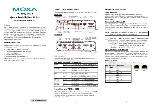
P/N: 1802024010011V2401/2402Quick Installation GuideSecond Edition, March 2011OverviewThe V2401/2402 Series embedded computers are based on the Intel Atom N270 x86 processor, and feature four RS-232/422/485 serial ports, eight RS-232 serial ports, dual Gigabit LAN ports, six USB 2.0 hosts, and a CompactFlash socket. The V2401 computer provides VGA, DVI, and LVDS outputs, and the V2402 computer provides both VGA and DVI outputs, making them particularly well-suited for industrial applications such as SCADA and manufacturing automation.Package ChecklistBefore installing the V2401/2402, verify that the package contains the following items: • V2401/2402 embedded computer• Terminal block to power jack converter • Wall mounting kit• Quick installation guide•Documentation and software CDNOTE: Please notify your sales representative if any of the above items are missing or damaged.V2401/2402 Panel Layout The following figures show the panel layouts of the V2401/2402. Front ViewRear ViewLED IndicatorsThe following table describes the LED indicators located on the front panel of the V2401/2402.Installing the V2401/2402The V2401/2402 can be DIN-rail mounted, wall mounted and VESA mounted. Some mounting kits may need to be purchased separately. Refer to the Hardware User's Manual for detailed installation instructions.Connector DescriptionPower ConnectorConnect the 9 to 36 VDC LPS or Class 2 power line to theV2401/2402’s terminal block. If the power is supplied properly, the Power LED will light up. The OS is ready when the Ready LED glows a solid green.Grounding the V2401/2402Grounding and wire routing help limit the effects of noise due to electromagnetic interference (EMI). Run the ground connection from the ground screw to the grounding surface prior to connecting the power.NOTE This product is intended to be mounted to a well-grounded mounting surface, such as a metal panel.SG: The Shielded Ground (sometimes called Protected Ground) contact is the right most of the 3-pin power terminal block connector when viewed from the angle shown here. Connect the SG wire to an appropriate grounded metal surface.VGA, DVI and LVDS OutputsThe V2401/2402 comes with a D-Sub 15-pin female connector for a VGA monitor; it also comes with a DVI-I connector for the DVI display. The V2401 has even an LVDS interface to connect an LVDS display. These output interfaces are all located at the front panel. Use the proper cable to connect.Ethernet PortsThe 10/100/1000 Mbps Ethernet ports use RJ45 connectors./supportThe Americas: +1-714-528-6777 (toll-free: 1-888-669-2872)Europe: +49-89-3 70 03 99-0 Asia-Pacific: +886-2-8919-1230China: +86-21-5258-9955 (toll-free: 800-820-5036)2010 Moxa Inc., All Rights ReservedSerial PortsThe serial ports use DB9 connectors. Each port can be configured by software for RS-232, RS-422, or RS-485. The pin assignments for the ports are shown in the following table:The V2401 includes a serial connector on the front panel; it can connect eight serial devices with a 68-pin VHDC connector and transmit the data with the RS-232 interface. CompactFlash SlotThe V2401/2402 has an internal CompactFlash slot for storage expansion. It supports CF Type-I/II with DMA mode. To install a CompactFlash card, remove the outer cover, and then insert the CF card in the socket. When finished, push the cover into the socket and fasten the screws. USB HostsThe V2401/2402 has four USB 2.0 hosts on the front panel and two USB 2.0 hosts on the rear panel. Users may use these USB ports to connect flash disks for storing large amounts of data. Audio InterfaceThe V2401/2402 comes with an audio input and an audio output, allowing users to connect a speaker or an earphone. DI/DOThe V2401/2402 comes with 4-ch digital input and 4-ch digital output in the terminal block connectors.Reset ButtonPress the “Reset Button” on the rear panel of the V2401/2402, the system will reboot automatically. The Ready LED will blink on and off for the first 5 seconds, and then maintain a steady glow once the system has rebooted.Real-time ClockThe V2401/2402’s real-time clock is powered by a lithium battery. We strongly recommend that you do not replace the lithiumbattery without help from a qualified Moxa support engineer. If you need to change the battery, contact the Moxa RMA service team.Powering on the V2401/2402To power on the V2401/2402, connect the “terminal block to power jack converter” to the V2401/2402’s DC terminal block (located on the side panel), and then connect the power adaptor. Press the Power Button to turn on the computer. Note that the Shielded Ground wire should be connected to the top pin of the terminal block. It takes about 30 seconds for the system to boot up. Once the system is ready, the Power LED will light up.Connecting the V2401/2402 to a PCPower on the V2401/2402 computer after connecting a monitor, keyboard, and mouse, and verifying that the power source is ready. Once the operating system boots up, the first step is to configure the Ethernet interface. The factory default settings for theV2401/2402’s LANs are show below. (XPE models uses DHCP) Configuring the Ethernet InterfaceLinux users should follow these steps:If you use the console cable to configure Network settings for the first time, use the following commands to edit the interfaces file:#ifdown –a//Disable LAN1~LAN2 interface first, before you reconfigure the LAN settings. LAN1 = eth0, LAN2 = eth1//#vi /etc/network/interfaces//check the LAN interface first//After the boot setting of the LAN interface has been modified, use the following commands to activate the LAN settings immediately:#sync; ifup –aWinCE 6.0 users should follow these steps:1. Go to [Start] → [Settings] → [Network and Dial-UpConnections]. You will see two network interfaces. 2. Right click the LAN interface to be configured and click[property]. A configuration window will pop-up.3. Click OK after inputting the proper IP address and netmask. WinXPE users should follow these steps:1. Go to [Start] → [Network Connections].2. Right-click Network Connections , click Properties , selectInternet Protocol (TCP/IP), and then click Properties . 3. Click OK after inputting the proper IP address and netmask. NOTE: Refer to the User’s Manual for other configuration information.。
Hardware Reference Design BK2401/BK2421 硬件参考设计V3.0Beken Corporation博通集成电路(上海)有限公司中国上海张江高科技园区科苑路1278号3A电话: (86)21 5108 6811传真: (86)21 6087 1277文档含博通(BEKEN)公司保密信息,非经书面许可,不可外传更改记录目录1.本文档主要内容 (5)2.NANO DONGLE原理图设计 (6)2.1.原理图和BOM表 (6)B MCU选择 (9)2.3.射频匹配电路 (9)2.4.BK2401/BK2421电源滤波 (9)2.5.16M晶体选择 (9)2.5.116M晶体指标 (9)2.5.2使用MCU晶体作为输入 (10)3.NANO DONGLE版图(PCB LAYOUT)设计 (11)3.1.板材的选择 (11)3.2.天线L AYOUT (11)3.3.射频匹配电路L AYOUT (11)3.4.BK2401/BK2421芯片L AYOUT (12)3.5. 3.3V电源L AYOUT (12)3.6.16M晶体L AYOUT (13)3.7.控制线L AYOUT (14)B MCU L AYOUT (14)4.如何将NANO PCB 应用到NORMAL MODULE中 (15)5. 2.4G PCB 天线设计 (17)5.1.小尺寸N ANO D ONGLE用PIFA天线设计 (17)5.2.更大尺寸N ORMAL M ODULE用PIFA天线设计 (20)5.3.更大尺寸N ORMAL M ODULE用W IGGLE天线设计 (23)6.最终原理图和版图 CHECKLIST (26)图表图表 1 NANO的USB MCU原理图---------------------------------------------------------------------------------------------- 6图表 2 NANO的BK2401/BK2421 MODULE原理图 ----------------------------------------------------------------------- 7图表 3 NANO DONGLE的完整BOM-------------------------------------------------------------------------------------------- 8图表 4 NANO DONGLE 匹配电路LAYOUT ---------------------------------------------------------------------------------- 11图表5 BK2401/BK2421芯片LAYOUT---------------------------------------------------------------------------------------- 12图表6 3.3V电源 LAYOUT-------------------------------------------------------------------------------------------------------- 12图表7 NANO DONGLE 和NORMAL MODULE晶体 LAYOUT ---------------------------------------------------------- 13图表8 SPI线LAYOUT ------------------------------------------------------------------------------------------------------------- 14图表9 NORMAL MODULE 匹配电路LAYOUT ----------------------------------------------------------------------------- 15图表11 NANO DONGLE PIFA天线 -------------------------------------------------------------------------------------------- 17图表12 NANO DONGLE PIFA天线S11 -------------------------------------------------------------------------------------- 18图表13 NANO DONGLE PIFA天线增益 ------------------------------------------------------------------------------------- 19图表14 NORMAL MODULE PIFA天线 --------------------------------------------------------------------------------------- 20图表15 NORMAL MODULE PIFA天线S11---------------------------------------------------------------------------------- 21图表16 NORMAL MODULE PIFA天线增益--------------------------------------------------------------------------------- 22图表17 NORMAL MODULE WIGGLE天线 ---------------------------------------------------------------------------------- 23图表18 NORMAL MODULE WIGGLE天线S11----------------------------------------------------------------------------- 24图表19 NORMAL MODULE WIGGLE天线增益---------------------------------------------------------------------------- 251. 本文档主要内容本文档描述了用BK2401/BK2421如何简单快速地实现无线终端的硬件设计,该硬件方案可广泛应用于计算机周边及消费类无线终端设备中,如无线键鼠、无线语音、无线遥控及监视等。
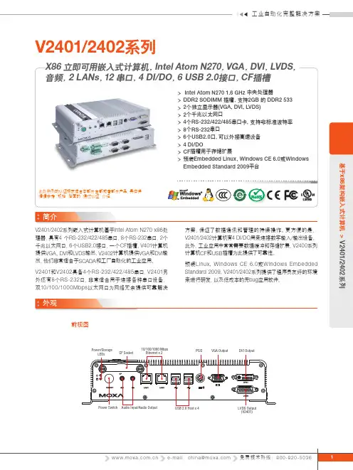
基于x86架构嵌入式计算机> V2401/2402系列V2401/2402系列V2401/2402系列嵌入式计算机基于Intel Atom N270 x86处理器,具有4 个RS-232/422/485串口,8个RS-232串口,2个千兆以太网口,6个USB2.0接口,一个CF插槽。
V401计算机提供VGA, DVI和LVDS输出,V2402计算机提供VGA和DVI输出,他们非常适合于SCADA和工厂自动化的工业应用。
V2401和V2402具备4个RS-232/422/485串口,V2401另外还有8个RS-232口,非常适合用于连接各种串口设备,双10/100/1000Mbps以太网口为网络冗余提供可靠解决方案,保证了数据通讯和管理的持续操作。
更方便的是,V2401/2402计算机有4 DI/DO用来连接数字输入/输出设备。
此外,工业应用中常常需要数据缓冲和存储扩展,V2400系列计算机CF和USB插槽为此提供了可靠性。
预装Linux, Windows CE 6.0或Windows EmbeddedStandard 2009, V2401/2402系列提供了程序员友好的环境来进行研发,以及低成本的无bug应用软件。
简介外观前视图此处所列的认证标志适合本部分全部或者部分产品,具体详情请参考“规格”后面的“通过认证”介绍。
Power/Storage 10/100/1000 Mbps(V2401)系列硬件规格计算机CPU:Intel Atom N270 1.6 GHz 处理器操作系统(预装):Linux, Windows CE 6.0 or WindowsEmbedded Standard 2009系统芯片组:Intel 945GSE + ICH7-MBIOS:8 Mbit Flash BIOS, SPI type,支持ACPI功能FSB:400/533 MHz系统内存:1 x 200-pin DDR2 SODIMM 插槽,支持DDR2533高达2GB,内置1GBUSB:6个兼容USB2.0接口,A型接头,支持系统导入存储内置:2 GB CompactFlash 用于存储 OS扩展:CompactFlash插槽用于CF卡扩展,支持DMA模式I/II型CF插槽HDD支持:SATA-150接头用于HDD扩展其他外接设备KB/MS:1PS/2界面,支持标准PS/2键盘和Y型线缆的鼠标音频:HD音频,带线路输入和线路输出接口显示器图像控制器:Intel® Gen 2.5集成图像引擎,250 MHz corerender clock and 200 MHz core display clock at 1.05-Vcore VoltageVGA界面:DB15 母式连接器LVDS界面:板载HIROSE DF13-40DP-1.25 V接头(仅对V2401 )DVI界面:DVI-I连接器(chrontel CH7307 SDVO to DVItransmitter)以太网界面LAN: 2个自侦测10/100/1000 Mbps以太网口(RJ45)串口界面串口标准:• 4 RS-232/422/485口*, 软件可选(DB9 孔式)• 8 RS-232口, (68-针 VHDC 接头)* COM1端口引脚9信号可以被选择作为0 V(默认), +5 V, 或跳线至 +12 VESD保护:4KV对所有信号串口通讯参数数据位:5, 6, 7, 8停止位:1, 1.5, 2奇偶校验:None, Even, Odd, Space, Mark流向控制:RTS/CTS, XON/XOFF, 用于RS-485的ADDC®(自动数据导向控制)波特率:50 bps 至 921.6 Kbps(支持非标准波特率详细请参考用户手册)串口信号RS-232:TxD, RxD, DTR, DSR, RTS, CTS, DCD, GNDRS-422:TxD+, TxD-, RxD+, RxD-, GNDRS-485-4w:TxD+, TxD-, RxD+, RxD-, GNDRS-485-2w:Data+, Data-, GND数字输入输入通道:4, source type基于x86架构嵌入式计算机 >V2401/2402系列软件规格LinuxDistribution :Debian Lenny 5.0Kernel 版本:2.6.26协议栈:TCP , UDP , IPv4, SNMP V1, ICMP , ARP , HTTP , CHAP , PAP , SSH 1.0/2.0, SSL, DHCP , NTP , NFS, Telnet, FTP , PPP , PPPoE 文件系统:EXT2系统工具:bash, busybox, login, telnet, ftp, ssh, openbsdinetd, apt, apt-utils, dpkg, grub, udevtelnetd :telnet Server daemon ftpd :FTP server daemon sshd :secure shell server Apache :web server daemon, supporting PHP and XML openvpn :virtual private network service manager iptables :防火墙服务管理器NAT :网络地址翻译pppd :dial in/out over serial port daemon & PPPoE pppoe :PPP over ethernet tftp/tftpd :Trivial fi le transfer protocol client/server snmpd :snmpd agent daemon usbmount :支持 USB PnP DHCP Client :dhcp3-client cron :用于管理常规后台程序进程grep :NU grep, egrep, and fgrep minicom :友好串口通讯程序watchdog :软件看门狗inetd :TCP 服务器管理程序应用程序开发环境:GNU Make 3.8.1 (GNU make utility to maintain groups of programs)自动脚本配置:autoconf 2.13gcc :GNU C compiler g++:GNU C++ compiler libc6-dev :GNU C library (development libraries and headers)Perl :Pratical Extraction and Report Language Vim :Vi IMproved (enhanced vi editor)Windows Embedded CE 6.0版本:Windows Embedded CE 6.0 R3系统工具:Windows command shell, telnet, ftp 文件系统:FAT (on-board fl ash)协议栈:TCP , UDP , IPv4, SNMP V2, ICMP , IGMP , ARP , HTTP , CHAP , PAP , SSL, DHCP , SNTP , SMTP , Telnet, FTP , PPPTelnet 服务器:允许通过标准Telnet 客户端进行远程管理FTP 服务器:用于网络上主机之间进行文件传输File Server :允许客户端通过网络访问文件和资源(Microsoft ®Wincows ® CE)Web Server (httpd):包括 ASP , ISAPI Secure Socket Layer 支持, SSL 2, SSL 3, 以及 Transport Layer Security (TLS/SSL 3.1) public key-based protocols, 和Web Administration ISAPI Extensions.Dial-up Networking Service :RAS 客户端API 和PPP , 支持 Extensible Authentication Protocol (EAP)和RAS scripting.看门狗服务:在指定时间内通过CPU 硬件实现CPU 重启(通过调用MOXA 库函数来触发)应用程序开发环境:• Moxa WinCE 6.0 SDK输入电压:15Hz 下0 到 5 VDC 数字输入层:• 逻辑层 0:Close~ GND • 逻辑层1:Open连接类型:接线端子数字输出输出通道:4, source type, 0 ~5 VDC输出电流:最大每个通道20 mA 输出电压:• 逻辑 0:0-0.55 V • 逻辑 1:4.2-5.0 V连接类型:接线端子LED系统:电源,存储LAN :00M/Link x 2, 1000M/Link x 2 (在连接器上)开关和按钮电源开关:on/off (前面板)重启按钮:热启动(后面板)物理特性外壳:铝重量:• V2401:2.1 kg • V2402:2 kg 尺寸:无安装附件:250 x 57 x 152 mm (9.84 x 2.24 x 5.98 in)有安装附件:275 x 63 x 152 mm (10.83 x 2.48 x 5.98 in)安装:导轨,壁挂,VESA环境需求操作温度:-10 至 60 ˚C (14 至 140 ˚F)操作湿度:5 至 95% RH 存储温度:-40 至 85 ˚C (-40 至 185 ˚F)防抖:5 g rms @ IEC-68-2-34, random wave, 5-500 Hz, 1 hr/axis 防震:50 g @ IEC-68-2-27, half sine wave, 11 ms电源需求输入电压:9 至36 VDC (3-pin terminal block for V+, V-,SG)电源功耗:26 W (不带 LVDS 输出)**************@24VDC720mA@36VDC通过认证EMC :CE, FCC, CCC Safety :UL/cUL, LVD, CCC 绿色产品:RoHS, CRoHS, WEEE可靠性自动触发重启:内置 WDT (看门狗时钟) supporting 1-255 level time interval system reset, 可编程软件保修保修期:3年详情访问:/warranty基于x86架构嵌入式计算机 >V2401/2402系列订购信息可选型号V2401-CE :x86架构嵌入式计算机,Intel Atom N270, VGA, LVDS, DVI, 音频, 2 网口, 12 串口, 4 DI/DO, 6 USB 2.0, CF 卡插槽,WinCE 6.0V2401-XPE :x86架构嵌入式计算机,Intel Atom N270, VGA, LVDS, DVI, Audio, 2 网口, 12 串口, 4 DI/DOs, 6 USB 2.0, CF 卡插槽, Windows Embedded Standard 2009V2401-LX :x86架构嵌入式计算机,Intel Atom N270, VGA, LVDS, DVI, 音频, 2网口, 12串口, 4DI/DO, 6 USB2.0, CF 卡插槽,Linux 2.6V2402-CE :x86架构嵌入式计算机,Intel Atom N270, VGA, DVI, 音频,2网口, 4串口, 4DI/DO, 6 USB2.0, CF 卡插槽, WinCE 6.0V2402-XPE :x86架构嵌入式计算机,Intel Atom N270, VGA, DVI, 音频,2网口, 4串口, 4DI/DO, 6 USB2.0, CF 卡插槽, Windows Embedded Standard 2009V2402-LX :x86架构嵌入式计算机,Intel Atom N270, VGA, DVI, 音频, 2网口, 4串口, 4DI/DO, 6 USB2.0, CF 卡插槽, Linux 2.6可选配件(可单独选购)CBL-M68M9x8-100:8口RS-232线缆,VHDC 接头PWR-24250-DT-S1:电源适配器PWC-C7US-2B-183:2针接头电源线,美式插头PWC-C7EU-2B-183:2针接头电源线,欧式插头PWC-C7UK-2B-183:2针接头电源线,英式插头PWC-C7AU-2B-183:2针接头电源线,澳洲插头PWC-C7CN-2B-183:2针接头电源线,中式插头FK-75125-01:硬盘安装包DK-DC50131-01:导轨安装套件终端服务器:Microsoft 终端服务器客户端应用(mstsc.exe)COM+ Services :The next evolution of Microsoft Component Object Model (COM) and Microsoft Transaction Server (MTS).计算机浏览器服务:Windows 通过微软网络推出的计算机浏览功能。
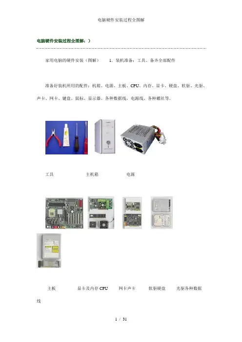
电脑硬件安装过程全图解:)家用电脑的硬件安装(图解)1.装机准备:工具、备齐全部配件准备好装机所用的配件:机箱、电源、主板、CPU、内存、显卡、硬盘、软驱、光驱、声卡、网卡、键盘、鼠标、显示器、各种数据线,电源线、各种螺丝等。
工具主机箱电源主板显卡及内存CPU 网卡声卡软驱硬盘光驱各种数据线2.安装主板部件:CPU(1G、1.7G、2.0G….)、散热片和风扇安装好后的CPU 将散热风扇安装在散热片的顶部最后一步,将CPU风扇的电源线接到主板上3针的CPU风扇电源接头上即可。
如下图所示。
3. 安装内存(128M、256M、512M……)现在常用的内存有168线的SDRAM内存和184线的DDR SDRAM内存两种,其主要外观区别在于SDRAM内存金手指上有两个缺口,而DDR SDRAM内存只有一个缺口。
下面给出了两种内存条的图例。
SDRAM DDR SDRAM图中圆圈表示缺口下面就以184线的DDR SDRAM内存安装为例讲解。
第一步,安装内存前先要将内存插槽两端的白色卡子向两边扳动,将其打开,这样才能将内存插入。
然后再插入内存条,内存条的1个凹槽必须直线对准内存插槽上的1个凸点(隔断)。
第二步,再向下按入内存,在按的时候需要稍稍用力,如下图所示。
第三步,以使紧压内存的两个白色的固定杆确保内存条被固定住,即完成内存的安装。
4. 安装电源(AT、ATX电源如下面如示)一般情况下,我们在购买机箱的时侯可以买已装好了电源的机箱。
不过,有时机箱自带的电源品质太差,或者不能满足特定要求,则需要更换电源。
安装电源很简单,先将电源放进机箱上的电源位,并将电源上的螺丝固定孔与机箱上的固定孔对正。
然后再先拧上一颗螺钉(固定住电源),最后将3颗螺钉孔对正位置,再拧上剩下的螺钉即可。
小知识:ATX电源提供多组插头,其中主要是20芯的主板插头、4芯的驱动器插头和4芯的小驱动器专用插头。
20芯的主板插头只有一个且具有方向性,可以有效地防止误插,插头上还带有固定装置可以钩住主板上的插座,不至于让接头松动导致主板在工作状态下突然断电。
1Battery power cable, attached with battery detection cableCâble d’alimentation par batterie, joint au câble de détection de batterie2(2) Cable glands for Input/Output connection(2) Presse-étoupes pour connexions d’E/S 3Installation manual Manuel d’installation4Rack kit for 19-inch enclosures Kit de montage pour rack 19 pouces5Stabilizer bracket (4 screws included)Stabilisateur (4 vis fournies)For use with UPS models / Pour utilisation avec les modèles d’ASI : 9SX8KiPM, 9SX11KiPM, 9PX8KPM, 9PX11KPM, 9PX8KiPM, 9PX11KiPM, 9PX6KiPM31, 9PX8KiPM31, 9PX11KiPM31.Operating temperature / Température de fonctionnement : 0°C-40°C.1Input AC/Output DC terminal blocks Borniers d’entrée AC/sortie DC2Connector for battery modules (to the UPS and to the battery modules) Connecteurs pour modules batteries (vers l’UPS et vers les modules batteries)3Connector for automatic recognition of the Supercharger (to the UPS and to the battery modules)Connecteurs de reconnaissance automatique du Supercharger (vers l’UPS et vers les modules batteries)4LED On: when charging only /uniquement pendant la rechargeSet EBM manually: Battery settings External battery Manual EBM set.Régler manuellement les EBM : Réglages batterie Batterie externe Réglage EBM manuel.Refer to the battery manufacturer’s instructions regarding specific battery precautions.Consultez les instructions dufournisseur de batterie concernant les précautions spécifiques à la batterie.Set Ah manually: Battery settings External battery Manual battery set.Régler les Ah manuellement : Réglages batterie Batterie externe Réglage Ah manuel.External battery / Batterie externe configuration (50Ah – 400Ah / 240VDC)Automatic recognition of the Supercharger / Reconnaissance automatique du Supercharger :Recommended upstream protection / Protection amont recommandée to Normal AC source vers la source Normal AC2 poles circuit breaker D curve - 20ADisjoncteur 2 pôles courbe D - 20ARecommended battery protection / Protection batterie recommandée GBat +Bat -to batteryvers la batterie2 poles circuit breaker - 300V - 60ADisjoncteur 2 pôles - 300V - 60AT erminal BorneFunction FonctionT erminal wire size rating T ailles de fil du bornier Minimum wire size T aille minimum de filTightening torqueCouple de serrageL1N(L2)Input AC 0.5-6 mm 2 (20-10 AWG) 4 mm 2 (12 AWG) 75°C 10 lb in / 1.13 Nm (+)(-)Output DC2.5-16 mm 2 (14-6 AWG)16 mm 2 (6 AWG) 90°C10 lb in / 1.13 NmCopper wire, solid or stranded / Fil de cuivre, plein ou tressé.Recommended cable cross-sections / Sections de câble recommandées US installations only: to reduce the risk of fire, connect only to a circuit provided with 20A maximum branch circuit overcurrent protection in accordance with the National Electrical Code, ANSI/NFPA 70.US installations only: to reduce the risk of fire, connect only to a circuit provided with 60A maximum branch circuit overcurrent protection in accordance with the National Electrical Code, ANSI/NFPA 70.Disconnection and overcurrent protection devices shall be provided by others for permanently connected AC input and DC output circuits.Les dispositifs de déconnexion et de protection contre les surintensités doivent être fournis par les tiers pour les circuits d’entrée en régime alternatif et de sortie en régime continu qui sont branchés en permanence.。
巡更硬件安装和设置说明书-CAL-FENGHAI.-(YICAI)-Company One1巡更软硬件的安装和设置说明书软件安装由于巡更系统大部分是用于考核保安人员巡查工作的,而其管理人员也不一定是专业的计算机工作者,因此在研发的过程中充分考虑了应用的简单和便捷性,使之易学易懂。
在Windows 98/2000/XP/Vista系统下运行光盘上的,并按照提示完成软件安装。
注:软件安装的最后阶段会出现硬件驱动程序的安装提示,点击其<仍然继续>按钮。
另外,仅有一少部分用户的电脑系统软件缺少windows或office补丁,用户可以从网络升级上获得这部分内容,或者重新卸载掉office重新安装即可消除,或者点击取消可进入界面。
软件安装完成后在电脑桌面新增《巡更软件》图标:,双击该图标进入登陆界面。
初始安装的软件缺省用户名为:admin,密码不需输入,点击<确认>按钮直接进入系统主界面。
注:管理人员可以设置操作员密码,通过密码才可以登陆软件,这样可以有效避免无关人员有意或无意修改系统数据。
主界面上包含5个图标:<读取记录><报表><基础数据><参数><校正时间>,当鼠标停留在这5个图标上时,功能提示区给出简短的提示说明。
首次安装的软件,用户应该首先点击“主界面”上<系统设置>,图标,进入系统设置界面。
系统设置界面系统设置界面的功能包括:巡检器型号选择、通讯接口检测、软件版本设定等功能。
注:该软件可以选择多种应用语言环境,适合全球客户使用,软件安装时会自动匹配操作系统语言,一般不需人为干预。
选择巡检器型号,应点击<选择型号>按钮,来确定巡检器及其通讯端口。
在单位一栏中填写用户单位名称,比如:西安钧安电子科技有限公司删除 6 个月以前的记录,是指:在未来的应用中,巡更软件会自动删除较早以前的数据。
此处根据客户自身情况选择即可。
射束遮挡射束被烟雾干扰1.0 技术指标•待机电流:DS240:18.0 -2.0VDC接收器:24.0VDC 时为45mA 发射器:24.0VDC 时为20mA DS241:10.25VDC接收器:12.0VDC 时为50mA 发射器:12.0VDC 时为20mA •接收器报警电流:DS240:24.0VDC 时为60mA DS241:12.0VDC 时为75mA•发射器与接收器的间距:9.2-106.8米•系统间距:系统间距不应大于18.3米。
UL 认证的间距为60英尺。
•角度偏转:镜片可内部水平转动±90°,垂直调整±10°•灵敏度:灵敏度:可选择射束模糊度达百分之20,30,40,50,60或70•报警接点:报警接点:常开接点间的额定值在D C 阻抗负载时最大为1A,60VDC 。
不要与电容性和电感性负载一同使用。
•故障接点:故障接点:常闭接点间的额定值在D C 阻抗负载时最大为1A,60VDC 。
不要与电容性和电感性负载一同使用。
•辅助报警接点:辅助报警接点:“C ”型(N O ,C ,N C )接点间的额定值在DC 阻抗负载时最大为1A,60VDC 。
不要与电容性和电感性负载一同使用。
•防拆开关:接收器:带故障接点的防拆开关。
发射器:取下外壳时,防拆开关将中断发射。
•系统信号处理:传统的4线系统。
不能与带报警确认功能的系统一同使用。
•信号延迟:火警 = 可选30秒或5秒故障 = 20±2秒•温度:温度:存放与工作温度为-30°C - +54°C •安装:安装:此探测器安装于4英寸的方盒或8角盒中。
•认证:UL S3019ULC CS692MSFM Permit #1943NY City MEA Acceptance #MEA274-93-E CSFM #7260-1062:106FM Job #OX2A9.AY•标准配件:DIS2000远程测试/显示板和测试线•可选:DIS-240远程显示板,TK-240测试套件,AL240调校灯,TC2000测试线。
电脑硬件安装说明书一、前言感谢您购买我们的电脑硬件产品。
本安装说明书旨在帮助您正确、安全地安装和使用电脑硬件。
请在使用前仔细阅读本指南,并按照指导进行操作,以保证您的电脑硬件安装顺利进行。
二、准备工作1. 了解硬件安装位置:在开始安装之前,您需要了解硬件的安装位置。
请将电脑断电,并确保电源线从插座上拔下。
2. 工具准备:准备一把螺丝刀、一根电组线和一块防静电手腕带。
螺丝刀将用于拆卸电脑外壳,电组线将用于连接硬件,而防静电手腕带则能有效防止静电对电脑硬件的损害。
3. 静电防护:静电可能对电脑硬件造成损害。
在安装过程中,您应保证自己身体干燥,且穿着棉质衣服,以确保静电最小化。
此外,将电脑放在无静电的地方,远离静电产生的电器。
三、硬件安装步骤1. 打开电脑外壳:使用螺丝刀拆卸电脑外壳。
请注意,不同品牌的电脑外壳开启方式可能不同,请参照您所购买电脑的说明书。
2. 定位硬件插槽:根据您所购买的硬件类型(如内存、显卡、硬盘等),找到对应的插槽。
插槽通常位于主板上,注明有标识或者颜色代码。
3. 加装内存:将内存插槽上的保护盖取下,注意触摸金属接点时不要使用手指直接接触,以免静电损坏内存芯片。
将内存块沿着插槽的角度轻插进插槽中,然后用适当的力按下内存块,直到卡口扣上。
4. 安装显卡:找到主板上的PCI-E插槽,将显卡轻轻插入插槽中,确保插槽的连接部分与显卡接口匹配。
然后将显卡固定在电脑箱体上,将螺丝拧紧。
5. 连接硬盘:将硬盘插入到硬盘插槽中,并通过数据线将硬盘与主板连接。
然后将硬盘与电源连接,确保硬盘电源线和数据线连接牢固。
6. 检查连接:在完成硬件安装后,检查所有连接是否牢固。
确保内存、显卡和硬盘等硬件连接到位,并且所有数据线和电源线插头牢固无松动。
7. 关闭电脑外壳:重新安装电脑外壳,并将螺丝拧紧,以确保外壳牢固稳定。
四、启动和测试完成硬件安装后,您可以重新连接电脑电源,并启动电脑。
在启动过程中,请注意电脑是否能正常运行,并检查硬件是否被正确识别。