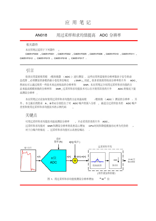
用过采样和求均值提高ADC分辨率
- 格式:pdf
- 大小:2.40 MB
- 文档页数:20
利用过采样技术提高ADC 测量微弱信号时的分辨率 1. 引言 随着科学技术的发展,人们对宏观和微观世界逐步了解,越来越多领域(物理学、化学、天文学、军事雷达、地震学、生物医学等)的微弱信号需要被检测,例如:弱磁、弱光、微震动、小位移、心电、脑电等[1~3]。
测控技术发展到现在,微弱信号检测技术已经相对成熟,基本上采用以下两种方法来实现:一种是先将信号放大滤波,再用低或中分辨率的ADC 进行采样,转化为数字信号后,再做信号处理,另一种是使用高分辨率ADC ,对微弱信号直接采样,再进行数字信号处理。
两种方法各有千秋,也都有自己的缺点。
前一种方法,ADC 要求不高,特别是现在大部分微处理器都集成有低或中分辨率的ADC ,大大节省了开支,但是增加了繁琐的模拟电路。
后一种方法省去了模拟电路,但是对ADC 性能要求高,虽然∑-△ADC 发展很快,已经可以做到24位分辨率,价格也相对低廉,但是它是用速度和芯片面积换取的高精度[4],导致采样率做不高,特别是用于多通道采样时,由于建立时间长,采样率还会显著降低,因此,它一般用于低频信号的单通道测量,满足大多数的应用场合。
而本文提出的方案,可以绕过上述两种方法的缺点,利用两者的优点实现微弱信号的高精度测量。
过采样技术是提高测控系统分辨率的常用方法,已经被广泛应用于各个领域。
例如,过采样成功抑制了多用户CDMA 系统中相互正交用户码接收机(A Mutually Orthogonal Usercode-Receiver ,AMOUR )的噪声[5~6],提高了光流估计(optical flow estimation ,OFE )的精度[7],改善了正交频分复用(OFDM )信号的峰-均比[8]等。
但是,这些过采样技术应用的前提是采样前的信号幅值能与ADC 的输入范围相当。
而用ADC 采集微弱信号时,直接使用过采样技术提高不了精度,而且由于信号幅值远小于ADC 的输入范围,它的有效位数还会减小,使精度随之下降。

AN2668Application noteImproving STM32F101xx and STM32F103xxADC resolution by oversamplingIntroductionThe STMicroelectronics Medium- and High-density STM32F101xx and STM32F103xxCortex™-M3 based microcontrollers come with 12-bit enhanced ADC sampling with a rateup to Msamples/s. In most applications, this resolution is sufficient, but in some cases wherehigher accuracy is required, the concept of oversampling and decimating the input signalcan be implemented to save the use of an external ADC solution and to reduce theapplication consumption.This application note gives two methods to improve ADC resolution. These techniques arebased on the same principle: oversampling the input signal with the maximum 1 MHz ADCcapability and decimating the input signal to enhance its resolution.The method and the firmware given within this application note apply to both Medium- andHigh-density STM32F10xxx products. Some specific hints are given at the end of theapplication note to take advantage of the Medium- and High-density STM32F103xxperformance line devices and of the High-density STM32F101xx access line devices.This application note is split into two main parts: the first one describes how oversamplingincreases the ADC-specified resolution while the second describes the guidelines toimplement the different methods available and gives the firmware flowchart of theirimplementation on the STM32F101xx and STM32F103xx devices.July 2008 Rev 11/21Contents AN2668Contents1Definition of ADC signal-to-noise ratio . . . . . . . . . . . . . . . . . . . . . . . . . . 4 2Nyquist theorem and oversampling . . . . . . . . . . . . . . . . . . . . . . . . . . . . 53Oversampling using white noise . . . . . . . . . . . . . . . . . . . . . . . . . . . . . . . 63.1SNR of oversampled signal with white input noise . . . . . . . . . . . . . . . . . . . 63.2Decimation . . . . . . . . . . . . . . . . . . . . . . . . . . . . . . . . . . . . . . . . . . . . . . . . . 63.3When is this method efficient? . . . . . . . . . . . . . . . . . . . . . . . . . . . . . . . . . . 73.4Method implementation on the STM32F10xxx devices . . . . . . . . . . . . . . . 83.4.1Oversampling using a white noise firmware flowchart . . . . . . . . . . . . . . . 93.4.2Oversampling using white noise result evaluation . . . . . . . . . . . . . . . . . 104Oversampling using triangular dither . . . . . . . . . . . . . . . . . . . . . . . . . . 124.1When does this method work? . . . . . . . . . . . . . . . . . . . . . . . . . . . . . . . . . 124.2Method implementation on STM32F10xxx devices . . . . . . . . . . . . . . . . . 13 5Comparing the first and second methods . . . . . . . . . . . . . . . . . . . . . . 156Hints . . . . . . . . . . . . . . . . . . . . . . . . . . . . . . . . . . . . . . . . . . . . . . . . . . . . . 166.1What is the maximum number of bits that can be added tothe on-chip ADC resolution? . . . . . . . . . . . . . . . . . . . . . . . . . . . . . . . . . . 166.2Taking advantage of High-density STM32F10xxx devices . . . . . . . . . . . . 166.3Taking advantage of the Medium- and High-density performance line(STM32F103xx) devices 17Appendix A Quantization error . . . . . . . . . . . . . . . . . . . . . . . . . . . . . . . . . . . . . . . 18 Revision history . . . . . . . . . . . . . . . . . . . . . . . . . . . . . . . . . . . . . . . . . . . . . . . . . . . . 202/21AN2668List of figures List of figuresFigure 1.Oversampling effect on the quantization noise. . . . . . . . . . . . . . . . . . . . . . . . . . . . . . . . . . . 6 Figure 2.Histogram analysis. . . . . . . . . . . . . . . . . . . . . . . . . . . . . . . . . . . . . . . . . . . . . . . . . . . . . . . . 8 Figure 3.Histogram analysis for DC = 1.65 V . . . . . . . . . . . . . . . . . . . . . . . . . . . . . . . . . . . . . . . . . . . 9 Figure 4.Oversampling using a white noise flowchart. . . . . . . . . . . . . . . . . . . . . . . . . . . . . . . . . . . . 10 Figure 5.Ramp samples with 1 additional bit . . . . . . . . . . . . . . . . . . . . . . . . . . . . . . . . . . . . . . . . . . 11 Figure 6.Ramp samples with 2 additional bits . . . . . . . . . . . . . . . . . . . . . . . . . . . . . . . . . . . . . . . . . 11 Figure 7.How to perform oversampling by adding a triangular signal . . . . . . . . . . . . . . . . . . . . . . . 12 Figure 8.Hardware requirements of oversampling by adding a triangular signal . . . . . . . . . . . . . . . 13 Figure 9.Oversampling using triangular dither flowchart. . . . . . . . . . . . . . . . . . . . . . . . . . . . . . . . . . 14 Figure 10.Oversampling effect on the quantization error . . . . . . . . . . . . . . . . . . . . . . . . . . . . . . . . . . 183/21Definition of ADC signal-to-noise ratio AN26684/211 Definition of ADC signal-to-noise ratioThe ADC gives a representation of an analog signal among a finite number of digital words.Since the digital domain is represented by a finite number of words which have to present acontinuous signal, the conversion step introduces the quantization error function of the ADCinput range and resolution.For an ideal ADC, the quantization error is between ±0.5 LSB. In the case where the inputsignal is varying through many levels between samples, and the sampling rate is notsynchronized with the input frequency, the quantization error can be considered as a whitenoise whose energy is uniformly spread from the DC domain to half of the samplingfrequency. Please refer to Appendix A for more details regarding the calculation of itsdensity.The SNR (signal-to-noise ratio) is the ratio of the ADC noise to the input signal power. Foran ideal ADC, it is assumed that the SNR is equal to the quantization noise (no other noisesource is considered) to the input signal. It is demonstrated that for a full-scale sinusoidalsignal, the ADC SNR is maximum and given by the following formula:, where N is the ADC resolution.It is can be easily noticed that when the SNR increases, the ADC effective number of bitsincreases.For a real ADC, different error sources should be considered: offset, gain, INL (integralnonlinear) and DNL (differential nonlinear). A brief description of these errors can be foundin the STM32F101xx and STM32F103xx datasheets. They degrade the ideal ADCresolution. In this case, we speak of real effective number of bits.Improving the SNR involves an enhancement of the ADC effective number of bits.The following section demonstrates that sampling the input signal with higher rates than theNyquist frequency improves the SNR. The Nyquist frequency is introduced in the nextparagraph.SNR dB 6.02N 1.76+=AN2668Nyquist theorem and oversampling 2 Nyquist theorem and oversamplingThe Nyquist theorem states that in order to be able to reconstruct the analog input signal,the signal should be sampled at a rate f S (sampling frequency) that is greater than twice themaximum frequency component of the input signal.Not respecting the Nyquist theorem causes aliasing effects and the analog signal cannot befully reconstructed from the input samples. Therefore, in most applications, a low-pass filteris required at the ADC input to filter frequencies lower than half the sampling frequency. It isdifficult to handle the filter constraints with low sampling frequencies.Oversampling consists in sampling the input analog signal at rates higher than the Nyquistfrequency limit, filtering the samples and reducing the sample rate by decimation. Using thismethod relaxes the anti-aliasing low-pass filter constraints.5/216/213Oversampling using white noise 3.1 SNR of oversampled signal with white input noiseLet us assume that the quantization noise is assimilated to white noise. Then its powerdensity is uniformly distributed between DC and half the Nyquist frequency. This powerdensity is independent of the sampling frequency.When sampling at higher rates, the quantization noise is spread over the bandwidth of thesampling frequency. Figure 1.Oversampling effect on the quantization noiseAccording to Figure 1, when sampling the input signal at higher rates, the same noisepower, represented by the area of the green rectangle, is spread over a bandwidth equal tothe sampling frequency which is much greater than the signal bandwidth fm. Only arelatively small fraction of the total noise power falls in the [–fm, fm] band , and the noisepower outside the signal band can be greatly attenuated with a digital low-pass filter.Reducing the quantization noise enhances the signal-to-noise ratio and, consequently, theADC effective number of bits. Oversampling the input signal OSR times faster than theNyquist frequency gives the following SNRIt can be concluded that each doubling of the sampling frequency will lower the in-bandnoise by 3 dB, and increase the measurement resolution by 1/2 bit. Therefore, 6dB SNRgain is required to add 1 resolution bit to the ADC.In general, if p additional bits are required by the application then, the ADC samplingfrequency should be at least:, where F S is the current ADC sampling frequency used.3.2 DecimationThe conventional meaning of averaging is adding m samples and dividing the result by m.Averaging several data from an ADC measurement is equivalent to a low-pass filter whichattenuates the signal fluctuation and noise. The average method is often used to smoothand remove speaks from the input signal.Note that normal averaging does not increase the resolution of the conversion because thesum of m N-bit samples divided per m is an N-bit representation of the sample.F f m - f m f S = 2.f m -2.f m F f m - f m f S = 2.N.f m-2.N.f m PSD PSDSame area Input signalQuantization errorPSD = Power signal densityai14937SNR OVS 6.02N 1.76+⋅10OSR ()log +=F OVS 4pF S =Decimation is an averaging method. When combined with oversampling, decimationimproves the ADC resolution.In fact, adding 4p ADC N-bit samples, gives a representation of the signal on N+2p bits. Inorder to have p additional effective bits, the sum is shifted to the right by p bits.This FIR filter with equal filter coefficients enables the user to filter the oversamplingfrequency by giving an output sample computed from the OSR input samples.The oversampling method limits the maximum input frequency bandwidth. In fact, in thecase of the STM32F10xxx, signals having components up to 500 kHz can be processed bythe ADC. If for example, two additional resolution bits are required, then the maximum inputfrequency that can be entered is 500 kHz/16 = 31.25 kHz when oversampling using whitenoise.3.3 When is this method efficient?For the oversampling and decimating method to work properly, the following requirementsmust be satisfied:●There should be some noise in the input signal. This noise must approximate whitenoise with a uniform power spectral density over the frequency band of interest.●The noise amplitude must be sufficient to toggle the input signal randomly from sampleto sample by an amount of at least 1 LSB. Otherwise, the input samples would have thesame representation and the sum and average operations would not give any extraresolution. In most applications, the internal ADC thermal noise and the input signalnoise are sufficient to use this method. In the case where the thermal noise does nothave a high-enough amplitude to toggle the input signal randomly, then artificial whitenoise should be injected into the input signal. This operation is referred to as“dithering”. Regarding this point, two questions can be raised. The first is “How toevaluate the ADC noise and test its Gaussian criteria?” and “How to generate whitenoise if needed?”– A practical way of detecting the Gaussian criteria of the input signal noise is to see the distribution of a clean DC signal over the ADC codes. The histogram methodcan be used to verify if the input noise follows a Gaussian distribution. Theexample in Figure2 shows two possible situations.7/218/21 Figure 2.Histogram analysis –In the case where external noise dither should be added to the input signal, thenthe thermal noise generated by a diode or a resistor can be injected into the input signal.–The input noise should not correlate with the useful input signal and the inputsignal should have equal probability to be between two adjacent ADC codes. This means that for systems using feedback process, this method does not work.3.4 Method implementation on the STM32F10xxx devicesThis method describes the different steps undertaken to implement and test theoversampling method on the STM32F10xxx devices.According to the previous section, in order to make this solution work properly, there should be some white noise to make the input signal toggle randomly by 1/2 LSB. For this, the application environment noise should be considered.The first step consists in computing the STM32F10xxx ADC thermal noise to conclude if external white noise should be injected into the input signal. In a typical application board, the computed noise does not include only the ADC internal noise but also the possible noise generated by the different board components and the layout. Therefore, this evaluation depends on the application board but the methodology remains the same.The histogram method is used for different DC input voltages. This input voltage is sampled a large number of times (example 5000). The related distribution can be easily interpreted using a spreadsheet.For example, for a 1.65 V DC input voltage applied on the STM3210B-EVAL evaluation board, the histogram shown in Figure 3 is detected.ADC codes N N+1N+2N–1N–2Histogram for a signal with white noise ADC codesN N+1N+2N–1N–2Histogram for a signal without white noiseai14938Figure 3.Histogram analysis for DC = 1.65 Vai14939 The ADC thermal noise can be computed from this histogram (though this can be shown, itis not the objective of this application note and details are not offered here).In order to carry on this ADC noise test, the user should do the following:●uncomment the line #define Themal_Noise_Measure in the oversampling.h file●configure the Total_Samples_Number which is the number of ADC conversionoperations. It should be smaller than 65535. The DMA channel is configured to storethe number of ADC samples in a RAM buffer. At the end of the transfer, an interrupt isgenerated and the number of occurrences of each ADC code is computed●In order to compute the occurrence of the ADC codes, a variable giving the relevantADC codes is definedWhen the code is run, Relevant_ADC_Samples ADC samples and their correspondingnumber of occurrences are displayed on the HyperTerminal. The HyperTerminalconfiguration is 8-bit data, no parity, 115 200 baud rate. If the effective number of ADCsamples found is smaller than the defined Relevant_ADC_Samples variable, then 0 isdisplayed for both ADC code and ADC code occurrence. The user can capture them andbuild a histogram.3.4.1 Oversampling using a white noise firmware flowchartThe STM32F10xxx on-chip ADC conversion frequency is fixed to 1 MHz. The ADC DMAchannel is configured to transfer the number of oversampled inputs from the ADC dataregister to a buffer in RAM. This transfer is configured to occur one time. At the end of theDMA transfer, an interrupt is triggered and the oversampled result is computed.The STM32F10xxx general-purpose timer TIM2 is used to generate the input signalsampling frequency. For this, the TIM2 reference clock is configured at 1 µs. Its perioddetermines the input signal sampling period. It is defined in the oversampling.h file as#define Input_Signal_Sampling_Period. When the TIM2 update interrupt istriggered, the DMA is re-enabled and the converted ADC values can be treated. Figure4summarizes the implemented functionality.9/2110/21 Figure 4.Oversampling using a white noise flowchartThe oversampled data are computed in the DMA transfer complete interrupt. For synchronization reasons, it is recommended to read it in the second TIM2 interrupt.Note that with this implementation, the TIM2 period should be greater than the time required by the ADC to convert OSR samples, and greater than the ADC interrupt execution time.If the sampling frequency required by the application is exactly OSR µs, then the user is not required to use Timer TIM2 to generate the input sampling frequency. However, the DMA should be configured to be functional in continuous mode and the DMA transfer complete interrupt should be updated accordingly. The oversampled data are usually computed in the DMA transfer complete interrupt.3.4.2 Oversampling using white noise result evaluationIn order to evaluate the oversampling method, the user should uncomment the #define Oversampling_Test line and configure the number of samples with the enhanced resolution.When this line is uncommented, a buffer is created in RAM to store the oversampled data. The buffer contents are then displayed on the HyperTerminal. The HyperTerminalconfiguration should be 8-bit data, no parity and 115 200 baud rate. The user can capture them into a txt file and then compare the expected results to the real ones.In order to evaluate the new enhanced ADC, a ramp with a 50 Hz frequency and a 1Vamplitude is input into the ADC and sampled using the oversampling algorithm every 50 µs.The firmware example related to this method is located in the WhiteNoiseMethod folder.Sampling period = TIM2 periodADC period = 1 µs TIM2 update interruptClear flagEnable DMA Time t<=1µsDMA transfer complete interrrupt Clear DMA Interrupt pending bit Compute the oversampled resultUpdate DMA counter and pointerDisable DMAai14940AN2668Oversampling using white noise11/21Figure 5.Ramp samples with 1 additional bit Figure 6.Ramp samples with 2 additional bitsThe oversampling algorithm using white noise is run with the same ramp (50 Hz frequencyand 1 V amplitude). Both Figure 5 and Figure 6 give the ADC oversampled data as afunction of time in µs. Figure 5 is the result of adding one bit while Figure 6 is the result ofadding two additional bits to the ADC on-chip resolution.When the ramp is sampled without using any extra software resolution, with a 3.3 Vreference supply, 1 V corresponds to the digital value 1250.When one additional bit is added, 1 V is sampled as 2500 and when two additional bits areadded, 1 V is sampled as 5000.This means that the environment contains enough noise for this method to work.50 H/1 V - 1 additional bit300025002000150010005000306090120150180210240270300330360390ai1494250 H/1 V - 2 additional bits60005000400030002000100004182123164205246287328369410451492533574615656697738779ai1494212/214 Oversampling using triangular ditherAssuming that the input signal is between two successive quantization steps q0 and q1during the oversampling period, then the converter may convert it either to q0 or q1. Addingextra p bits of resolution means determining the relative position of the input signal betweenq0 and q1.With the addition of an appropriate triangular signal, the quantizer generates a series of q1sand q0s. Averaging the q1 occurrences over a given interval determines the relative positionof the input signal between the lower and the higher quantization steps.The theory states that the best results are achieved when dithering the input signal using atriangular waveform with a period of OSR times the ADC sampling period and an amplitudeof n+0.5LSB where n = 0,1,2,3.The theory behind this methods is quite complicated, so that Figure 7 serves as an exampleto illustrate how this method works. In this example, the ADC on-chip resolution is 3 andthree extra bits are added by firmware. The input signal is assumed to have an amplitude ofq0+ 0.6LSB (q0 = 6 in this example). In order to add three additional bits, the input signal issampled 2.23 times (16 times).If the input signal is not correlated with the triangular waveform, then it is demonstrated thatthe gain in the SNR is equal toTherefore, each doubling of the sampling frequency improves the SNR by 6dB and adds 1ADC bit resolution.In general, in order to add p-bit extra resolution, the oversampling frequency should beequal to4.1 When does this method work?In order to make this method work, the input signal should not vary by more than ±0.5LSBduring the oversampling period and should not correlate with the triangular dither signal.SNR Gain 20.OSR 2-------------⎝⎠⎛⎞log =F OVS 2.2pF S =4.2 Method implementation on STM32F10xxx devicesIn order to implement the second solution, the following is needed:●An operational amplifier to perform the sum of the input signal and the triangularwaveform. For this, an op-amp inverter/summing stage is required. The ST componentLMV321 can be used.●Triangular waveform with a period of OSR times the ADC conversion rate. The user caneither use a signal generator or one of the STM32F10xxx on-chip timers and an RCnetwork to generate this triangular signal. Indeed, the on-chip timer generates a PWMsignal with a duty cycle varying from 0 to 100%. This PWM output can be filtered withan RC filter to generate a triangular signal varying from 0 to V DD. In order to generatean amplitude of 0.5LSB, then the output is first passed through a capacitor (to cut theDC component) and then divided by the prescaler R2/R3 (see Figure8). This prescaleris equal to the ADC number of words.●The input signal should not be changed after the op-amp. For this reason, R1 should beequal to R3.●The sum of the input signal and the triangular dither is inverted. For this purpose, a3.3V offset is required on the positive entry of the op-amp. After the oversampled dataare computed, this offset is subtracted to give the input signal estimation with extraresolution.The STM32F10xxx on-chip ADC conversion frequency is fixed at 1 MHz. The ADC DMAchannel is configured to transfer the number of oversampled inputs from the ADC dataregister to a buffer in RAM. This transfer is configured to occur one time. At the end of theDMA transfer, an interrupt is triggered and the oversampled result is computed.The STM32F10xxx general-purpose timer TIM2 is used to generate the input signalsampling frequency. For this, the TIM2 reference clock base is configured at 1 µs. Its perioddetermines the input signal sampling period. It is defined in the oversampling.h file by#define Input_Signal_Sampling_Period.The triangular dither is generated using Timer TIM3 configured in PWM mode by updatingthe Capture Compare Register CCR1. Timer TIM3 period should be equal to the ADCconversion rate and CCR1 should be updated OSR times where OSR is the oversamplingfactor. In order to do this, the possible CCR1 values are first computed and stored into aRAM buffer, then DMA transfer is used to update the CCR1 register, removing the need forinterrupts.Note that the ADC conversion rate limits the oversampling factor. For example, in the casewhere the ADC is running at 1 MHz, the STM32F10xxx is operating at 56 MHz. In order to13/2114/21have a period of 1 µs, the auto-reload register of timer TIM3 should be equal to 55. Themaximum number of additional bits is then 4.When a TIM2 update interrupt is triggered, the ADC and TIM3 DMA are re-enabled and theconverted ADC values can be treated to compute the new sample with the extra resolutionbits. Figure 9 summarizes the implemented functionality.Figure 9.Oversampling using triangular dither flowchartFor this method to work, the input signal should not vary by more than ±0.5LSB during theoversampling period. This means that for an STM32F10xxx operating from a 3.3 V VDDpower supply, the maximum allowed variations of the input signal during the oversamplingperiod is ~0.4 mV .On the other side, a triangular waveform with an amplitude of 0.5LSB means a 0.4 mVamplitude when operating the STM32F10xxx from a 3.3 V power supply. The applicationenvironment must therefore not be very noisy. Any disturbance of the triangular waveformwill have an impact on the computed oversampled data.According to the implementation, the triangular waveform is generated by means of theSTM32F10xxx timer and an RC filter that cuts the 1 MHz timer frequency. The timer PWMoutput signal is integrated to provide a triangular signal with a 3.3 V amplitude. The divisionis done with the ratio R4/R2.The firmware related to this method is located in the TriangularDitherMethoddirectory.Sampling period = TIM2 periodADC period = 1 µsTIM2 Update interruptClear flagEnable ADC DMATime t<=1µADC DMA transfer complete interrupt Clear DMA Interrupt pending bit Compute the oversampled result Update ADC DMA counter and pointersDisable DMAEnable TIM3 DMA Update TIM3 DMA counter and pointersTIM 3 period = ADC period = 1 µsTIM3 CCR1 register varies during OSR period (OSR = 4 in this example)Input signal dithered with thetriangular signalInput signalai14945AN2668Comparing the first and second methods 15/215 Comparing the first and second methodsThe first method based on oversampling and averaging using white noise provides a half-bitadditional resolution for each doubling of the oversampling rate. The maximum inputfrequency is drastically decreased with the additional number of additional bits.For applications where this gain is sufficient, then it is a good choice. It requires thepresence of white noise in the input signal to make the signal toggle between two adjacentADC codes. In general, the ADC thermal noise is sufficient and there is no need to addexternal hardware to act as an external white noise source. This makes the solution morecost-effective.The second method based on dithering the input signal using a triangular waveform andcomputing its relative position between two quantized steps provides one more bit for eachdoubling of the oversampling rate. This is twice the improvement given by the first method.To make this method work, the input signal should not correlate with the triangular signaland should not have a variation greater than 0.5LSB during the oversampling period.However, external hardware is needed to add the input signal and the triangular waveform.Table 1 summarizes the main differences between the two methods. It is not possible to saythat one method is better than the other. Each method has its advantages and limitations.The user should select the one that better meets their application requirements (samplingfrequency, number of effective bits etc.).Table 1.Oversampling using white noise vs. oversampling using triangular ditherImplementation conditions Oversampling usingwhite noise Oversampling using triangular ditherOversampling factor to add p bits to he ADC on-chip resolution 4p 2.2pMaximum Input signal frequency f ADC max/(2.4p )f ADC max/(2.2.2p )Dither signal White noise with an amplitude of at least 1 LSB T riangular signal with an amplitudeof n+0.5LSBExternal hardwareExternal white noise source needed if the input signal noise is not sufficient T riangular waveform generator: anon-chip timer can be used.–In this case, an RC network isused to filter the PWM frequency–An op-amp is needed to add thetriangular waveform and the inputsignal。
过采样技术提升ADC采样精度其实原理很简单, 很容易明白, 怎样实现提高分辨率?假定环境条件: 10位ADC最小分辨电压1LSB 为1mv假定没有噪声引入的时候, ADC采样上的电压真实反映输入的电压, 那么小于1mv的话,如ADC在0.5mv是数据输出为0 我们现在用4倍过采样来, 提高1位的分辨率,当我们引入较大幅值的白噪声: 1.2mv振幅(大于1LSB), 并在白噪声的不断变化的情况下, 多次采样, 那么我们得到的结果有真实被测电压白噪声叠加电压叠加后电压ADC输出ADC代表电压0.5mv 1.2mv 1.7mv 1 1mv0.5mv 0.6mv 1.1mv 1 1mv0.5mv -0.6mv -0.1mv 0 0mv0.5mv -1.2mv -0.7mv 0 0mvADC的和为2mv, 那么平均值为: 2mv/4=0.5mv!!! 0.5mv就是我们想要得到的这里请留意, 我们平时做滤波的时候, 也是一样的操作喔! 那么为什么没有提高分辨率?????是因为, 我们做滑动滤波的时候, 把有用的小数部分扔掉了, 因为超出了字长啊, 那么0.5取整后就是0 了, 结果和没有过采样的时候一样是0 ,而过采样的方法时候是需要保留小数部分的, 所以用4个样本的值, 但最后除的不是4, 而是2! 那么就保留了部分小数部分, 而提高了分辨率!从另一角度来说, 变相把ADC的结果放大了2倍(0.5*2=1mv), 并用更长的字长表示新的ADC值,这时候, 1LSB(ADC输出的位0)就不是表示1mv了, 而是表示0.5mv, 而(ADC输出的位1)才是原来表示1mv的数据位,下面来看看一下数据的变化:ADC值相应位9 8 7 6 5 4 3 2 1 00.5mv测量值0 0 0 0 0 0 0 0 0 0 0mv(10位ADC的分辨率1mv,小于1mv无法分辨,所以输出值为0)叠加白噪声的4次过采样值的和0 0 0 0 0 0 0 0 1 0 2mv滑动平均滤波2mv/4次0 0 0 0 0 0 0 0 0 0 0mv(平均数, 对改善分辨率没作用)过采样插值2mv/2 0 0 0 0 0 0 0 0 0 0 1 2mv/2=0.5mv, 将这个数作为11位ADC值, 那么代表就是0.5mv这里我们提高了1位的ADC分辨率这样说应该就很简单明白了吧, 其实多出来的位上的数据, 是通过统计输入量的分布, 计算出来的,而不是硬件真正分辨率出来的, 引入噪声并大于1LSB, 目的就是要使微小的输入信号叠加到ADC能识别的程度(原ADC最小分辨率).理论来说, 如果ADC速度够快, 可以无限提高ADC的分辨率, 这是概率和统计的结果但是ADC的采样速度限制, 过采样令到最后能被采样的信号频率越来越低,就拿stm32的ADC来说, 12ADC, 过采样带来的提高和局限分辨率采样次数每秒采样次数12ADC 1 1M13ADC 4 250K。
基于过采样技术提高ADC分辨率的研究与实现很多应用场合需要使用模/数转换器ADC进行参数测量,这些应用所需要的分辨率取决于信号的动态范围、必须测量的参数的最小变化和信噪比SNR。
许多系统中既有很宽的动态范围又要求测量出参数的微小变化,因此就必须使用高分辨率的ADC。
然而,高分辨率的ADC器件价格昂贵,若使用价格相对低廉的具有较低分辨率的ADC器件,通过一些技术也达到较高的分辨率,则在工程应用中是非常受欢迎的。
过采样技术就可以提高模数转换的分辨率而实现该目很多应用场合需要使用模/数转换器ADC进行参数测量,这些应用所需要的分辨率取决于信号的动态范围、必须测量的参数的最小变化和信噪比SNR。
许多系统中既有很宽的动态范围又要求测量出参数的微小变化,因此就必须使用高分辨率的ADC。
然而,高分辨率的ADC 器件价格昂贵,若使用价格相对低廉的具有较低分辨率的ADC 器件,通过一些技术也达到较高的分辨率,则在工程应用中是非常受欢迎的。
过采样技术就可以提高模数转换的分辨率而实现该目的。
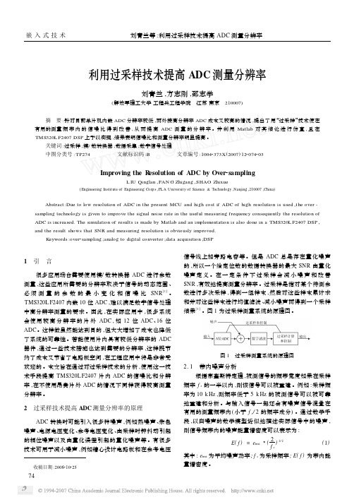
1 基本原理ADC 转换时可能引入很多种噪声,例如热噪声、杂色噪声、电源电压变化、参考电压变化、由采样时钟抖动引起的相位噪声以及由量化误差引起的量化噪声。
有很多技术可用于减小噪声,例如精心设计电路板和在参考电压信号线上加旁路电容等,但是ADC 总是存在量化噪声的,所以一个给定位数的数据转换器的最大SNR 由量化噪声定义。
在一定条件下过采样和求均值会减小噪声和改善SNR,这将有效地提高测量分辨率。
过采样指对某个待测参数,进行多次采样,得到一组样本,然后对这些样本累计求和并对这些样本进行均值滤波、减小噪声而得到一个采样结果。
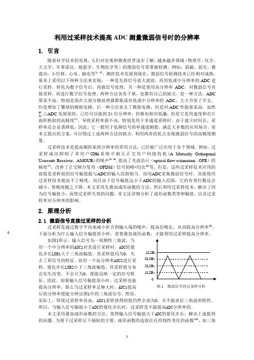
由奈奎斯特定理知:采样频率fs 允许重建位于采样频率一半以内的有用信号,如果采样频率为40kHz,则频率低于20kHz 的信号可以被可靠地重建和分析。
与输入信号一起,会有噪声信号混叠在有用的测量频带内(小于fs/2 的频率成分):erms 是平均噪声功率,fs 是采样频率,E(f)是带内ESD。
sigma-delta adc的量化过程Sigma-Delta ADC(Σ-Δ ADC)是一种常用的模数转换器,它通过采用过采样和噪声整形技术,实现了高精度的模拟信号数字化转换。
本文将介绍Sigma-Delta ADC的量化过程,以及其原理和应用。
让我们了解一下Σ-Δ ADC的基本原理。
Σ-Δ ADC可以看作是一个模拟滤波器和一个数字滤波器的级联,其中模拟滤波器用于滤除高频噪声,数字滤波器用于恢复被过采样信号中的模拟信号。
Σ-Δ ADC的核心思想是在过采样的基础上通过噪声整形技术将噪声推到高频区域,从而提高了系统的动态范围和分辨率。
在Σ-Δ ADC的量化过程中,首先将模拟信号通过一个比特数较高的模数转换器进行采样。
然后,通过一个积分器对模拟信号进行积分,并将积分结果与一个参考电平进行比较。
根据比较结果,Σ-Δ ADC会输出一个1或0的比特,表示模拟信号是否超过了参考电平。
为了更好地理解Σ-Δ ADC的量化过程,可以以一个简单的二进制Σ-Δ ADC为例进行说明。
假设该ADC的比特数为N,那么它将输出一个N位的二进制数。
在量化过程中,如果积分结果大于参考电平,则输出1,否则输出0。
通过这种方式,Σ-Δ ADC可以实现高精度的模拟信号转换。
在实际应用中,Σ-Δ ADC常常用于对低频信号的高精度采样,比如音频和传感器信号采集。
由于Σ-Δ ADC具有较高的动态范围和分辨率,能够抑制高频噪声和共模噪声,因此在音频处理和测量仪器等领域得到了广泛的应用。
除了以上的基本原理和应用外,Σ-Δ ADC还有一些进一步的发展和应用。
例如,Σ-Δ ADC可以通过多级嵌套的方式,实现更高的分辨率和更宽的动态范围。
此外,Σ-Δ ADC还可以结合数字滤波器,实现对不同频率的信号的处理和采样。
总结起来,Σ-Δ ADC是一种基于过采样和噪声整形技术的高精度模数转换器。
它的量化过程通过积分和比较实现,并通过输出二进制数来表示模拟信号的大小。