Pixel-matched holographic data storage with megabit pages
- 格式:pdf
- 大小:230.56 KB
- 文档页数:3

亚像素抓变算法halcon
亚像素抓变算法是HALCON图像处理软件中的一种算法,用于在像素级别上进行精确的位置检测和测量。
该算法通过对图像进行亚像素级别的插值,可以实现更高的检测精度和测量精度。
亚像素抓变算法的基本原理是在像素级别上对图像进行插值,以获得更高的分辨率。
在图像中,每个像素被视为一个区域,该算法通过对该区域进行插值,将其分为更小的子区域,并计算每个子区域的灰度值。
然后,通过比较子区域的灰度值,确定目标的精确位置。
亚像素抓变算法在图像处理中有广泛的应用,例如在机器视觉中用于检测和测量微小的特征,如边缘、角点等。
它可以提高检测和测量的精度,从而提高整个系统的性能。
亚像素抓变算法是HALCON图像处理软件中的一种算法,通过对图像进行亚像素级别的插值,实现精确的位置检测和测量。
它在机器视觉等领域有着广泛的应用。
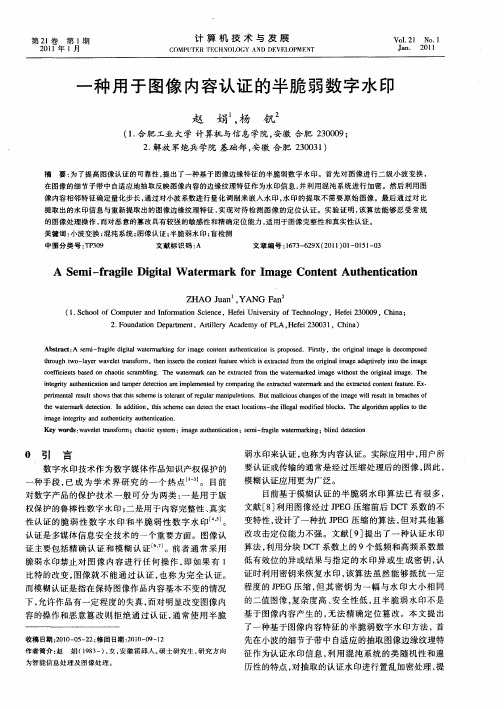
NOIL1SN3000ALUPA3000: 3 MegaPixel High Speed CMOS SensorFeatures•1696 x 1710 Active Pixels •8 m m x 8 m m Square Pixels •1.2 inch Optical Format•Monochrome or Color Digital Output •485 Frames per Second (fps) Frame Rate •64 On-Chip 8-Bit ADCs•32 Low −V oltage Digital Signaling (LVDS) Serial Outputs •Random Programmable Region of Interest (ROI) Readout •Pipelined and Triggered Global Shutter •Serial Peripheral Interface (SPI)•Dynamic Range Extended by Double Slope •Limited Supplies: Nominal 2.5 V and 3.3 V •0°C to 60°C Operational Temperature Range •369-Pin m PGA Package •1.1 W Power Dissipation•These Devices are Pb −Free and are RoHS Compliant Applications•High Speed Machine Vision •Holographic Data Storage •Motion Analysis•Intelligent Traffic System •Medical Imaging •Industrial ImagingDescriptionThe LUPA3000 is a high-speed CMOS image sensor with an image resolution of 1696 by 1710 pixels. The pixels are 8 m m x 8 m m in size and consist of high sensitivity 6T pipelined global shutter capability where integration during readout is possible. The LUPA3000 delivers 8-bit color or monochrome digital images with a 3 Megapixels resolution at 485 fps that makes this product ideal for high-speed vision machine, intelligent traffic system, and holographic data storage. The LUPA3000 captures complex high-speed events for traditional machine vision applications and various high-speed imaging applications.The LUPA3000 production package is housed in a 369-pin ceramic m PGA package and is available in a monochrome version or Bayer (RGB) patterned color filter array with micro lens. Contact your local ON Semiconductor representative for more information.ORDERING INFORMATIONMarketing Part NumberMono / ColorPackageNOIL1SN3000A-GDC Mono micro lens with glass 369−pin m PGANOIL1SE3000A-GDCColor micro lens with glassNOTE:Refer to Ordering Code Definition on page 54 for more information.Figure 1. LUPA3000 Package PhotoCONTENTSFeatures1 .....................................Applications1.................................Description1 ..................................Ordering Information1.........................Contents2 .................................... Specifications3................................Key Specifications3..........................Electrical Specifications4......................Overview6 ....................................Color Filter Array6...........................Spectral Response6...........................Sensor Architecture8...........................Image Sensor Core8..........................Analog Front End9...........................Data Block13.................................LVDS13 .....................................On−Chip BandGap Reference and Current Biasing17.Sequencer and Logic18.........................Serial Peripheral Interface (SPI )31...............Operating Modes32.............................Global Shutter Mode32.........................Image Sensor Timing and Readout34..............Pixel Timing34...............................Frame Rate and Windowing34...................Image Format and Readout Protocol36............Sensor Timing and Readout36...................Readout Modes37.............................Data Stream38................................Frame Overhead Time38........................Reduced ROT Readout Mode39..................FOT and ROT Pin Timing39....................Asynchronous Reset39.........................Startup Sequence40............................Additional Features41...........................Windowing41................................Sub Sampling41..............................Reverse Scan41...............................Multiple Windows41...........................Dual Slopes41................................Off-Chip FPN Correction42.....................Software FPN Correction43.....................Off-Chip PRNU Correction43...................Package Information44..........................Pin Definitions44.............................Pin Assignment49.............................Mechanical Specifications51....................Package Diagram52...........................Glass Lid54 ..................................Handling Precautions54.........................Limited Warranty54............................Return Material Authorization (RMA)54...........Acceptance Criteria Specification54...............Ordering Code Definition54......................Acronyms55 ...................................Glossary56 ....................................SPECIFICATIONS Key SpecificationsTable 1. GENERAL SPECIFICATIONSParameter SpecificationsActive pixels1696 (H) x 1710 (V)Pixel size8 m m x 8 m mPixel type6T pixel architectureData rate412 Mbps (32 serial LVDS outputs)Shutter type Pipelined and Triggered GlobalShutterFrame rate485 fps at full frameMaster clock206 MHzWindowing (ROI)Randomly programmable ROI readout. Implemented as scanning oflines or columns from an uploadedposition.ADC resolution8−bit, on−chipExtended dynamic range Double slope (up to 80 dB opticaldynamic range)Table 2. ELECTRO−OPTICAL SPECIFICATIONSParameter SpecificationsConversion gain39.2 m V/e-Full well charge27000 e-Responsivity1270 V.m2/W.s at 550 nm withmicro lensParasitic light sensitivity< 1/5000Dark noise21 e-Quantum efficiency (QE)x Fill−factor (FF)37% at 680 nm with micro lensFixed pattern noise (FPN)2% of Vsweep RMSPhoto responsenon−uniformity (PRNU)2.2% of VsignalDark signal277 mV/s at 25°CPower dissipation 1.1 W at 485 fpsTable 3. RECOMMENDED OPERATING RATINGST J (Note 2)Operating temperature range060°CTable 4. ABSOLUTE MAXIMUM RATINGS (Note 1)Symbol Description Min Max Units ABS (2.5 V supply group)ABS rating for 2.5 V supply group−0.5 3.0V ABS (3.3 V supply group)ABS rating for 3.3 V supply group−0.5 4.3VT S (Notes 3 and 4)ABS Storage temperature range−40+150°C ABS Storage humidity range590%RHElectrostatic Discharge (ESD)(Note 3)Human Body Model (HBM)2000V Charged Device Model (CDM)500VLU Latch−up LUPA3000 is not rated forlatch−upmAStresses exceeding Maximum Ratings may damage the device. Maximum Ratings are stress ratings only. Functional operation above the Recommended Operating Conditions is not implied. Extended exposure to stresses above the Recommended Operating Conditions may affect device reliability.1.Absolute maximum ratings are limits beyond which damage may occur.2.Operating ratings are conditions in which operation of the device is intended to be functional.3.ON Semiconductor recommends that customers become familiar with, and follow the procedures in JEDEC Standard JESD625−A.Refer to Application Note AN52561. Long term exposure toward the maximum storage temperature will accelerate color filter degradation.4.Caution needs to be taken to a void dried stains on the underside of the glass due to condensation. The glass lid glue is permeable and canabsorb moisture if the sensor is placed in a high % RH environment.Electrical SpecificationsExceeding maximum ratings may shorten the useful life of the device. User guidelines are not tested.Table 5. POWER SUPPLY RATINGS (Notes 1, 2 and 3)Limits in bold apply for T A= T MIN to T MAX, all other limits T A= +25°C. System speed = 50 MHz, Sensor clock = 200 MHz Symbol Power Supply Parameter Condition Min Typ Max Units V ANA, GND ANA Analog Supply Operating Voltage-5% 2.5+5%VDynamic Current Clock enabled, lux = 035mAPeak Current Row overhead time (ROT)100mA V DD, GND DD Digital Supply Operating Voltage-5% 2.5+5%VDynamic Current Clock enabled, lux = 01mAPeak Current Frame overhead time (FOT)80mAV DD_HS, GND DD_HS Digital Supplyhigh speedOperating Voltage-5% 2.5+5%VDynamic Current Clock enabled, lux = 0100mAPeak Current FOT60mAV PIX,GND PIX Pixel Supply Operating Voltage-5% 2.5+5%VPeak Current during FOT Transient duration = 2 m s210mAPeak Current during ROT Transient duration = 0.5 m s100mAV LVDS, GND LVDS LVDS Supply Operating Voltage-5% 2.5+5%V Dynamic Current Clock enabled, lux = 0170mAPeak Current ROT80mAV ADC, GND ADC ADC Supply Operating Voltage-5% 2.5+5%VDynamic Current Clock enabled, lux = 0150mAPeak Current Clock enabled, lux = 0275mA V RES Reset Supply Operating Voltage-5% 3.3+5%VPeak current during FOT Transient duration: 200 ns1000mA V RES_DS Reset dual slopesupplyOperating Voltage 1.8 2.5 3.5VV MEM_L (Note 4)Memory Elementlow level supplyOperating Voltage-5% 2.5+5%VPeak current during FOT Clock enabled, bright180mAV MEM_H Memory Elementhigh level supply Operating Voltage-5% 3.3+5%V Peak current during FOT90mAV PRECHARGE Pre_chargeDriver Supply Operating Voltage-10%0.4+10%V Peak Current during FOT Transient duration: 50 ns10mAV CM Common modevoltageOperating Voltage(Refer to Table 44 on page 29)0.9V1.All parameters are characterized for DC conditions after thermal equilibrium is established.2.Peak currents are measured without the load capacitor from the LDO (Low Dropout Regulator). The 100 nF capacitor bank is connectedto the pin in question.3.This device contains circuitry to protect the inputs against damage due to high static voltages or electric fields. However, take normalprecautions to avoid application of any voltages higher than the maximum rated voltages to this high impedance circuit.4.The V MEM_L power supply should have a sourcing and sinking current capability.Table 6. POWER DISSIPATION (Note 1)Power supply specifications according to Table 5.Symbol Parameter Condition Min Typ Max Units Dynamic Power Average power dissipation lux = 0, clock = 50 MHz0.8 1.1 1.4W Standby Power Power dissipation in standby lux = 0, No clock180mWTable 7. AC ELECTRICAL CHARACTERISTICS (Note 1)The following specifications apply for VDD = 2.5 VSymbol Parameter Condition Typ Max Units F CLK Input clock frequency fps = 485206MHz fps Frame rate Maximum clock speed485fps 1.All parameters are characterized for DC conditions after thermal equilibrium is established.Combining Power SuppliesEvery module in the image sensor has its own power supply and ground. The grounds can be combined externally, but not all power supply inputs may be combined. Some power supplies must be isolated to reduce electrical crosstalk and improve shielding, dynamic range, and output swing. Internal to the image sensor, the ground lines of each module are kept separate to improve shielding and electrical crosstalk between them.The LUPA3000 contains circuitry to protect the inputs against damage due to high static voltages or electric fields. However, take normal precautions to avoid voltages higher than the maximum rated voltages in this high-impedance circuit. All power supply pins should be decoupled to ground with a 100 nF capacitor. The Vpix and Vres_ds power are the most sensitive to power supply noise.The recommended combinations of supplies are:•Analog group of +2.5 V supply: V RES_DS, V ADC, V pix, V ANA•Digital Group of +2.5 V supply: V DD, V D_HS, V LVDS •The V MEM_L and V PRECHARGE supplies should have sinking and sourcing capability BiasingThe sensor requires three biasing resistors. Refer to Table8 for more information.For low frame rates (< 2000 fps), the PRECHARGE_BIAS_1 pins are connected directly with the VPRECHARGE pins. The DC level on the PRECHARGE_BIAS_1 pins acts as a power supply and must be decoupled.For higher frame rates, the duty cycle on VPRECHARGE is too high and the voltage drops. This causes the black level to shift compared to the low frame rate case. In higher frame rates, the voltage on PRECHARGE_BIAS_1 is buffered on the PCB and the buffered voltage is taken for VPRECHARGE. A second possibility is to make the biasing resistor larger until the correct DC level is reached. PRECHARGE_BIAS_2 must be left floating, because it is intended for testing purposes.Table 8. BIASING RESISTORSSignal Comment Related Module DC level Current_Ref_1Connect with 20 k W (1% prec.) to V AA. Decouple to GND AA Column amplifiers769 mV at 86 m A Current_Ref_2Connect with 50 k W (1% prec.) to GND ADC. No decoupling ADCs25 m A to gnd Precharge_Bias_1Connect with 90 k W (1% prec.) to V PIX. Decouple to Vpix with100nF.Pixel array0.45 V at 23 m A Precharge_Bias_2Leave floatingOVERVIEWThe datasheet describes the interfaces of the LUPA3000.The CMOS image sensor features synchronous shutter with a maximum frame rate of 485 fps at full resolution.The sensor contains 64 on-chip 8-bit ADCs operating at 25.75 Msamples/s each, resulting in an aggregate pixel rate of 1.4 Gigapix/s. The outputs of the 64 ADCs are multiplexed onto 32 LVDS serial links operating at 412Mbit/s each resulting in an aggregate date rate of 13.2Gbits. The 32 data channel LVDS interface allows a high data rate with limited number of pins. Each channel runs at 51.5 MSPS pixel rate, which results in 485 fps frame rate at full resolution. Higher frame rates are achieved by windowing, which is programmable over the SPI interface.All required clocks, control, and bias signals are generated on-chip. The incoming high speed clock is divided to generate the different low speed clocks required for sensor operation. The sensor generates all its bias signals from an internal bandgap reference. An on-chip sequencer generates all the required control signals for the image core, the ADCs,and the on-chip digital data processing path. The sequencer settings are stored in registers that can be programmed through the serial command interface. The sequencer supports windowed readout at frame rates up to 10000 fps.Color Filter ArrayThe color version of LUPA3000 is available in Bayer (RGB) patterned color filter array. The orientation of RGB and active pixel array [0,0] is shown in Figure 2.Figure 2. RGB BayerSpectral ResponseFigure 3 shows the spectral response of the mono and color versions of the LUPA3000. Figure 4 and Figure 5 on page 7 depict the micro lens behaviour for mono and color devices for mid range wavelengths.Figure 3. Mono and Color Spectral ResponseFigure 4. Micro Lens Behavior for MonoFigure 5. Micro Lens Behavior for ColorSENSOR ARCHITECTUREImage Sensor CoreThe LUPA3000 floor plan is shown in Figure 6. The sensor consists of the pixel array, column amplifiers, analog front end (AFE) consisting of programmable gain amplifier and ADCs, data block (not shown), sequencer, and LVDS transmitter and receivers. The image sensor of 1696 x 1710 active pixels is read out in progressive scan.The architecture enables programmable addressing in the x-direction in steps of 32 pixels, and in the y-direction in steps of one line. The starting point of the address can be uploaded by the SPI.The AFE prepares the signal for the digital data block when the data is multiplexed and prepared for the LVDS interface.NOTE:In Figure 7 on page 9, 32 pixels (1 kernel) are read out, where the most significant bit (MSB) isthe first bit out.3232Odd kernelsEven kernelsFigure 6. Sensor Floor PlanFigure 7. Column Multiplexing Scheme6T Pixel ArchitectureThe pixel architecture shown in Figure 8 features the global shutter combined with a high sensitivity and good parasitic light sensitivity (PLS). This pixel architecture is designed in an 8 m m x 8 m m pixel pitch and designed with a large fill factor to meet the electro-optical specifications as shown in Table 2 on page 3.Figure 8. Pixel SchematicFigure 9 displays the electro-optical response of theLUPA3000 6T pixels at V DD= 2.5 V.Figure 9. Electro−optical Response of LUPA3000 Pixel Analog Front EndProgrammable Gain Amplifiers(PGA)LUPA3000 includes analog PGA (before each of the 64 ADCs) to maximize sensor array signal levels to the ADC dynamic range. Six gain settings are available through the SPI register interface to allow 1x, 1.5x, 2x, 2.25x, 3x, or 4x gain.The entire AFE signal processing and ADC concept for the LUPA3000 chip is shown in Figure 10.The analog signal processing frontend circuits provide programmable gain level. They also convert the single ended pixel voltage from each column (as referenced to the user programmable black or dark reference level) to a unipolar differential signal for the PGA stages. This is followed by a conversion to a bipolar differential signal to maximize the ADC dynamic range and noise immunity.Figure 10. Analog Frontend and ADC ConceptTable 9. PROGRAMMABLE AMPLIFIERS GAIN SETTINGSRegister Address d73 Gain Level Comments Bit 2Bit 1Bit 000 01x POR default value00 1 1.5x01 0 2.0x01 1 2.25x10 0 3.0x10 1 4.0x11 x 3.0x Do not use (Redundant gain codes)The gain is set through bits 2:0 in register 73 (decimal). The gain register controls the gain setting globally for all64 PGA and ADC channels.A latency (delay) is incurred for the analog signal processing, PGA, and ADC stages. The total latency is 44 high-speed input clock delays. The output synchronization signals from the LVDS sync channel factor in this latency. Programmable Dark LevelAn SPI-controlled DAC provides the PGA with a dark level. This analog voltage corresponds with the all-zero output of the ADC. This dark level is tuned to optimally use the ADC range.The dark level coming from the pixels follow a Gaussian distribution. This distribution is visible in a dark image as the FPN. The spread on the distribution is influenced by the dark current and temperature. Typically the spread is 100mV peak-to-peak.The average dark level of this distribution depends on several parameters:•The processing corner•Tolerances on the pixel power supplies (Vpix, Vreset, Vmem_l, and Vmem_h)•Pixel timingThe combination of these parameters adds an offset to the dark level. The offset is in the order of magnitude of 200 mV.To allow off-chip FPN calibration, the full spread on the dark level is mapped inside the range of the ADC. To optimally use the input range of the ADC, the spread on the dark level is mapped as close as possible to the high level of the ADC’s input range.The default startup value of the dark level coming from the DAC is 1.5 V. This ensures that the spread on the dark level is completely mapped in the ADC range. The startup DAC dark level is not optimal. By taking a dark image after startup, the offset on the dark image histogram is measured. The offset from the optimal case is subtracted from the dark level coming from the DAC. This places the dark level distribution optimally inside the range of the ADC. Follow this procedure after every change in operation condition such as temperature, FOT timing, and ROT.Analog- to-Digital ConvertersLUPA3000 includes 64 pipelined 9-bit ADCs operating at approximately 25.75 mega samples per second (MSPS). Two ADCs are combined to provide digitized data to one of the 32 LVDS serialization channels. One of the ADC pair converts data from an ‘odd kernel’ of the LUPA3000 pixel array, the other from an ‘even kernel’. LUPA3000 only processes the eight MSBs of the converter to realize an improved noise performance 8-bit converter.分销商库存信息:ONSEMINOIL1SN3000A-GDC NOIL1SE3000A-GDC。

The SIGMA SD14Unique. Groundbreaking.And that’s just the three-layer,full-color image sensor.This digital camera is about toset a whole new standardfor image quality.THE SIGMA SD14DIGITAL SINGLE LENSREFLEX CAMERASIGMA CORPORATION 2-4-16, Kuriki, Asao-ku, Kawasaki-shi, Kanagawa, 215-8530 Japan T el: +81-44-989-7430 Fax: +81-44-989-7451 www.sigma-photo.co.jp SIGMA SD14 / DIGITAL SINGLE LENS REFLEX CAMERA : MAJOR SPECIFICATIONS The Appearance and Specifications are Subject to Change without Notice.• Power Grip: PG-21, • AC Adapter: SAC-2, • Remote Controller: RS-31, • Cable Release Switch: CR-21, • Electronic Flash: EF-500 DG SUPER, EF-500 DG ST , EM-140 DG OPTIONAL ACCESSORIES • Li-ion Battery Pack BP-21, • Battery charger BC-21, • USB Cable, • Video Cable, • Neck Strap, • Eye Cap, • Body Cap, • Eyepiece Cap, • SIGMA Photo Pro Disc, • SD14 Instruction Manual ACCESSORIES Operating T emperatureOperating Humidity Range 0 — +40°C 85% or Lower OPERATING ENVIRONMENTDimensions Weight 144mm/5.7"(W), 107.3mm/4.2"(H), 80.5mm/3.2"(D)700g/24.7 oz DIMENSIONS AND WEIGHT Protection Erase Protection of Single Images or All Images in a Folder or CF/Microdrive™ Card is Possible CF/Microdrive™ Card Format, All, Current Image IMAGE PROTECTION AND ERASE Drive Modes Continuous Shooting Speed Continuous Buffer [1] Single, [2] Continuous, [3] Self-Timer (2 sec./10 sec.) [4] Mirror Lock-Up High : 3 Frames/second, Medium : 3 Frames/second, Low : 3 Frames/second High : 6 Frames, Medium : 12 Frames, Low : 24 Frames DRIVE SYSTEM T op LCD Shutter Speed Display, Aperture Value Display, Exposure Meter Display, Shooting Capacity Display, Exposure Mode Display, AF Mode Display , Flash Mode Display, Battery Status Display, Flash Mode Display, Remote Controller Mode Display, Electronic Sound Setting, Extended Mode DISPLA Y Image Display Highlight Display Histogram [1] Single Frame Display, [2] Multi Display (9 Frames), [3] Zoom, [4] Slide Show Available Available PLA YBACKLCD Monitor Language English / Japanese / German / Chinese / French / Spanish / Italian / Korean MENU Type Monitor Size LCD PixelsCoverageBrightness TFT Color LCD Monitor 2.5"150,000100%Dim, Normal, Bright LCD MONITOR TypeBuilt-in Flash Guide No.Built-in Flash CoverageFlash Metering SystemFlash CompensationCompatible FlashgunsSync. T erminalConnectivity Built-in Flash GN1117mm Lens Focal Length S-TTL Auto Flash +- 3EV(1/3 Stop Increments)EF-500DG SUPER, EF-500DG ST , EM-140 DG Available Hot Shoe, PC Sync. T erminal FLASH Shutter Type Shutter Speed External Flash Sync.Self Timer Electronically Controlled Focal Plane Shutter 1/4000 - 30 sec. + Bulb X-Sync. (1/180)2 and 10 Seconds Duration SHUTTER Exif 2.21, DCF 2.0Lossless compression RAW data(12-bit), JPEG(Super High, High, Medium, Low)Consecutive, Auto-ResetUSB (USB2.0), Video Out (NTSC/PAL)Still Image FormatRecording ModeFile Size File Numbering Interfaces RECORDING SYSTEMRAW JPEG HighMediumLowSuper High / FineSuper High / Normal Super High / BasicHigh / FineHigh / NormalHigh / BasicMedium / FineMedium / NormalMedium / BasicLow / FineLow / NormalLow / Basic2,6401,7761,2964,6084,6084,6082,6402,6402,6401,7761,7761,7761,2961,2961,296x x x x x x x x x x x x x x x 1,7601,184 8643,0723,0723,0721,7601,7601,7601,1841,1841,184 864 864 86413.3 MB 6.6 MB 3.3 MB 7.5 MB 4.6 MB3.2 MB 3.3 MB 1.9 MB 1.3 MB 1.6 MB 0.9 MB 0.6 MB 0.8 MB 0.5 MB 0.3 MB Approx.Approx.Approx.Approx.Approx.Approx.Approx.Approx.Approx.Approx.Approx.Approx.Approx.Approx.Approx.Metering Systems Metering Range Exposure Control System ISO Sensitivity Exposure Compensation AE Lock Auto Bracketing 8 Segment TTL Full Aperture Metering[1] 8 segments Evaluative Metering, [2] Center Metering,[3] Center-Weighted Average MeteringEV 1 — 20 (50mm F1.4, ISO100)[P] Program AE (Program Shift is Possible),[S] Shutter Priority AE, [A] Aperture Priority AE,[M] Manual, S-TTL Flash AEISO : 100, 200, 400, 800, (1600 with Extended Mode)+- 3 EV (in 1/3 Stop Increments)AE Lock Button is Pressed, when Shutter Release Button isPressed Halfway1/3EV Stops Up to +- 3EV Appropriate Exposure,Under Exposure and Over Exposure EXPOSURE CONTROLAuto Focus Type AF PointAF Working RangeFocusing ModesAF Point SelectionActive AF point indicatorAF Assist LightFocus Lock TTL Phase Difference Detection System 5-Points (Center AF Point : Cross Type) EV 0 — +18 (ISO100) Single AF , Continuous AF (with AF Motion Prediction Function), Manual Automatic Selection, Manual Selection Superimposed in Viewfinder White Color AF Assist Light Shutter Release Halfway-Down Position AUTOFOCUS TypeFrame CoverageMagnificationEye pointDiopter Adjustment RangeFocusing ScreenMirrorViewfinder Information Depth of Field Preview Pentaprism SLR viewfinder 98% Vertical x 98% Horizontal 0.9x (50mm F1.4 - oo)18mm -3 dpt — +1.5 dpt Fixed, All Matt Screen Quick Return Flash Display, AF Information, AF Frame, Shutter Speed,Aperture Value, AE Lock, Auto Bracketing, ExposureCompensation, Exposure MeterDepth of Field Preview Button VIEWFINDERSettingsAuto White Balance 8 types (Auto, Sunlight, Shade, Overcast, Incandescent, Fluorescent, Flash and Custom)Auto White Balance with The Image Sensor WHITE BALANCEFormat Number of Pixels FOVEON X3® Direct Image Sensor(CMOS)T otal Pixel 14.45 MP 2688 x 1792 x 3Effective Pixel 14.06 MP 2652 x 1768 x 3IMAGE SENSOR FormatStorage MediaImage Sensor SizeCompatible LensesLens MountAngle of View AF / AE Digital SLR Camera Compact Flash™(Type I/II), Microdrive™,(FAT32 compatible)20.7 x 13.8mm Sigma SA Mount Interchangeable Lenses Sigma SA Bayonet Mount Equivalent to approx. 1.7 timesThe Focal Length of The Lens (for 35mm cameras)FORMATBatteryBattery Life (+20°C )Battery Life (0°C )Battery Check Li-Ion Battery Pack BP-21, Battery Charger BC-21, AC Adapter SAC-2 (Optional)Approx. 500Approx. 4003 Level Battery Status Display POWER SOURCECaution : T o ensure the correct and safe use of the product, be sure to read the User’s Manual Carefully prior to operation.Copyright© 2006 Sigma Corporation All Rights Reserved.。

1网络游戏开发—DirectX函数归纳总结23003李翔李森2DirectX目录1.D3D 基本框架 (1)创建D3D 对象 (2)获取显卡显示模式 (2)创建D3D 设备接口 (2)开始渲染和结束渲染 (2)清空图形绘制区 (2)屏幕反转 (2)2.绘制基本图形 (1)绘制基本图形 (4)灵活定点格式(FVF) (2)基本图元的绘制 (2)创建顶点缓冲区 (2)基本图元的绘制 (2)保存顶点 (2)设置渲染状态 (2)图形绘制 (2)索引缓冲 (4)顶点设置 (2)创建索引缓冲区 (2)保存顶点索引值 (2)索引图形绘制 (2)D3D 中的图形学 (4)D3D 中的向量 (2)D3D 中的矩阵 (2)D3D 中的平面 (2)3D3D 中的射线 (2)D3D 中的图形变换 (2)3.纹理 (4)从磁盘文件获取纹理 (2)设置当前要渲染的纹理 (2)设置纹理的渲染状态 (2)设置纹理采样属性 (2)从一张纹理图形中生成多级纹理 (2)包装纹理寻址 (2)镜像纹理寻址 (2)夹取纹理寻址 (2)边框颜色纹理寻址 (2)一次镜像纹理寻址 (2)纹理包装 (2)4.光照 (4)D3D 光照的基本实现 (4)顶点格式 (2)设置物体材质 (2)添加光源 (2)激活光照运算 (2)5.摄像机 (4)生成视图变换矩阵 (2)生成投影变换矩阵 (2)6.模型基础 (4)ID3DXMesh 接口基础 (2)ID3DXMesh 接口相关 (2)应用.X 文件 (2)7.游戏中的基本特效 (4)4检查硬件支持的深度缓冲区格式 (2)激活深度测试 (2)设置深度缓冲区更新 (2)设置深度测试函数 (2)激活Alpha 混合 (2)设置Alpha 混合计算方式 (2)设置Alpha 混合系数 (2)激活Alpha 测试 (2)设置Alpha 测试参考值 (2)设置Alpha 测试函数 (2)多边形填充模式 (2)查询设备是否支持多重采样 (2)启用多重采样的全景图形反锯齿 (2)设置多纹理混合方式 (2)激活雾化 (2)设置雾化计算方式 (2)设置雾的颜色 (2)设置雾的起始范围 (2)指数雾化浓度 (2)基于发散的雾化 (2)创建2D 字体 (2)绘制字体 (2)5创建3D 文字网格 (2)8.游戏控制................ . . . . . . . . . . . . . . . . . . . .4. . . . . . . . . . . . . . . . . . . . . . . . . . . . . . . . . . . . . . . ....DirectInput 实现键盘控制 (2)...........................................DirectInput 实现鼠标控制 (2)..........................................................鼠标键选 (2)9.游戏音乐音效 (4)6D3D基本框架创建D3D对象:Direct3DCreate9(D3D_SDK_VERSION)===============================================================================DirectX===============================================================================获取显卡显示模式:HRESULT GetAdapterDisplayMode(UINT Adapter, //指定显示卡序列号D3DDISPLAYMODE *pMode //存储显示模式的指针===============================================================================DirectX===============================================================================创建D3D设备接口:HRESULT CreateDevice(UINT Adapter, //显卡序列号D3DDEVTYPE DeviceType, //D3D 设备类型HWND hFocusWindow, //所属窗口句柄DWORD BehaviorFlags, //设备进行3D 运算方式D3DPRESENT_PARAMETERS *pPresentationParameters, //用于存储D3D 设备相关信息的指针IDirect3DDevice9 ** ppReturnedDeviceInterface //返回D3D 设备接口指针的地址);第二个参数DeviceType 取值:D3DDEVTYPE_HAL //硬件抽象层,通过显示硬件来完成图形渲染工作D3DDEVTYPE_REF //参考光栅器,一般用于测试显卡不支持的D3D 功能D3DDEVTYPE_SW //用于支持第三方软件第四个参数BehaviorFlags 取值:D3DCREATE_SOFTWARE_VERTEXPROCESSING //由D3D 软件进行顶点运算(常用)D3DCREATE_FPU_PRESERVE //激活双精度浮点运算或浮点运算异常检测,设置该项会降低系统性能D3DCREATE_MULTITHREADED //保___________d+_证D3D 是多线程安全的,设置该项会降低系统性能7D3DCREATE_MIXED_VERTEXPROCESSING //由混合方式进行顶点运算D3DCREATE_HARDWARE_VERTEXPROCESSING //由D3D 硬件进行顶点运算D3DCREATE_PUREDEVICE //禁用D3D 的Get*()函数,禁止D3D使用虚拟设备模拟顶点运算===============================================================================DirectX===============================================================================开始渲染和结束渲染:BeginScene(); //开始渲染……实际的渲染工作……EndScene(); //结束渲染注意:这两个函数必须成对出现,不允许交错和嵌套的发生,实际的渲染工作在这两个函数的中间进行。
超分辨测向理论及其性能优化技术超分辨测向理论及其性能优化技术超分辨测向(Super-Resolution,简称SR)是一种图像处理技术,它可以将低分辨率的图像转换成高分辨率的图像,从而提高图像的质量。
超分辨测向理论是一种有效的图像处理技术,它可以有效地提高图像的分辨率,从而提高图像的质量。
超分辨测向理论的基本原理是,通过分析低分辨率图像中的细节,恢复出高分辨率图像中的细节,从而提高图像的质量。
超分辨测向理论的核心思想是,通过分析低分辨率图像中的细节,恢复出高分辨率图像中的细节,从而提高图像的质量。
超分辨测向理论的实现方式有多种,其中最常用的是基于深度学习的方法。
深度学习方法可以通过分析大量的低分辨率图像,学习出图像中的细节,从而恢复出高分辨率图像中的细节,从而提高图像的质量。
超分辨测向理论的性能优化技术也有多种,其中最常用的是基于深度学习的技术。
深度学习技术可以通过分析大量的低分辨率图像,学习出图像中的细节,从而恢复出高分辨率图像中的细节,从而提高图像的质量。
此外,还可以使用图像增强技术,通过对图像进行增强,提高图像的质量。
另外,还可以使用图像处理技术,如图像去噪、图像滤波等,来提高图像的质量。
此外,还可以使用图像分割技术,将图像分割成多个小块,从而提高图像的质量。
总之,超分辨测向理论是一种有效的图像处理技术,它可以有效地提高图像的分辨率,从而提高图像的质量。
此外,还可以使用多种性能优化技术,如深度学习技术、图像增强技术、图像处理技术和图像分割技术,来提高图像的质量。
因此,超分辨测向理论是一种有效的图像处理技术,可以有效地提高图像的质量。
超像素分割算法(SLIC算法)
SLIC算法的核心思想是将图像空间和颜色空间相结合,通过将像素点聚类为超像素,实现图像的分割。
算法的流程如下:
1.初始化:选择超像素数量K,并进行初始位置的选择。
一种常用的初始化方法是均匀地将图像分成K个网格,并选取每个网格的中心点作为初始位置。
2. 迭代优化:对每个超像素中心点,使用k-means算法将其周围的像素分类到该超像素。
这里的距离度量不仅包括欧氏距离,还考虑了颜色相似性和空间距离的权重。
同时,还计算了每个像素点到最近超像素中心点的距离,用于后续的超像素合并操作。
3.超像素合并:根据像素点到最近超像素中心点的距离和相邻超像素之间的相似性,进行超像素的合并操作。
这样可以将尺寸较小的超像素合并为更大的超像素,使得图像分割更加连贯。
4.迭代优化:重复步骤2和步骤3,直到达到预设的迭代次数或者收敛为止。
SLIC算法有以下特点:
1. 快速有效:SLIC算法通过使用k-means算法进行迭代聚类,使得算法具有较高的效率。
同时,由于使用了颜色和空间信息,也能够获得更好的分割效果。
2.参数少:SLIC算法只需要设置一个参数,即超像素数量K,此外,还可以根据需要设置聚类的迭代次数。
3.保持图像边界:由于考虑了颜色相似性和空间距离的权重,在进行超像素合并操作时能够较好地保持图像的边界。
4.可扩展性:SLIC算法可以很容易地扩展到多通道的图像,同时也可以用于视频超像素分割。
总的来说,SLIC算法是一种快速有效的超像素分割算法,具有较好的分割效果。
通过合适的初始化和迭代次数,可以在保持图像细节的同时实现图像的快速分割。
October1,1997/Vol.22,No.19/OPTICS LETTERS1509 Pixel-matched holographic data storage with megabit pages R.M.Shelby,J.A.Hoffnagle,G.W.Burr,C.M.Jefferson,M.-P.Bernal,H.Coufal,R.K.Grygier,H.G¨unther,R.M.Macfarlane,and G.T.SincerboxIBM Almaden Research Center,650Harry Road,San Jose,California95120-6099Received June17,1997Digital data-page holograms consisting of102431024arrays of binary pixels have been stored andsubsequently retrieved with an optical exposure consistent with a data rate1Gbit͞s.Each input pixel wasprecisely registered with a single detector pixel,and a raw bit-error rate as low as2.431026was demonstratedwith global-threshold detection.To our knowledge,this is the first demonstration of the often-cited goal ofholographic data storage of megabit data pages and a gigabit-per-second data rate.©1997Optical Society ofAmericaDigital holographic data storage,first conceived nearly 30years ago,1,2has received a great deal of atten-tion recently.3–8This is due largely to the emer-gence of liquid-crystal spatial light modulator and CCD detector-array technologies,which provide suitable in-put and output and thus allow one to seriously consider holography for data storage.One important feature of holographic storage is its high degree of parallelism, which arises from the storage and retrieval of holo-grams consisting of two-dimensional arrays,or pages, of binary pixels.It is projected that holographic storage can take ad-vantage of this parallelism to achieve data rates in the gigabit-per-second(Gbit͞s)range.Both spatial light modulators and CCD’s are available with102431024 arrays of pixels and1-kHz frame rates,and these yield an attractive data rate of1Gbit͞s.If1000such pages could be stored in a volume with a cross section of roughly5mm,an areal density of4Gbits͞cm2would be achieved,which is very competitive with current magnetic storage technology.The raw bit-error rate (BER)must be better thanϳ1025,a level correctable to 10212with an acceptable overhead for error-correcting code.Although they are often-cited goals,6,8–10the storage and retrieval of megabit(Mbit)holograms at such an error rate have never been accomplished to our knowledge,nor has a demonstration of Gbit͞s readout. This is because the precise imaging of each input data pixel over the entire102431024array through the storage medium and onto the corresponding detector pixel requires resolution and distortion performance that is usually unobtainable with inexpensive optics. Furthermore,Mbit-per-page holographic storage de-mands very high optical quality of the storage medium and excellent fidelity of the holographic recording and reconstruction process.With the holographic storage tester described in Ref.6,a small number of Mbit data pages were stored and retrieved in iron-doped lithium niobate(LiNbO3) crystals.The high optical performance of this tester permits precise one-to-one pixel matching from input data mask to detector array,and decoding of the reconstructed data-page image with a simple global threshold yielded BER’s as low as2.431026.The holograms had a diffraction efficiency of h331025 to431024and could be read out with a1-ms exposure of the readout beam,yielding an effective optical data rate of1Gbit͞s.The input data pattern was provided by a chrome-on-glass transmission mask consisting of a two-dimensional array of pixel locations spaced9m m apart.At approximately half of the randomly selected locations a 4.5-m m square opening was etched into the chrome to represent a binary1pixel.The other half of the pixels represented0.The data pattern was imaged through the LiNbO3crystal onto a CCD detector array with two custom lenses of approximately 89-mm effective focal length in the usual4f Fourier holography configuration.The crystal was located approximately2cm behind the Fourier plane of the lens system.The optics produced a pixel-matched, unity-magnification image of the data mask on the Kodak CCD that consisted of a153631024array of 9-m m detector pixels.Two iron-doped LiNbO3crystals were used,each 15mm315mm38mm in size.The object beam entered through the15mm315mm face,and the reference beam at90±through one of the8mm3 15mm faces,after expansion with cylindrical optics to nearly fill the crystal volume.Both beams were o polarized.Both crystals were doped with0.02% iron and had an absorptivity of0.8cm21at514nm. We erased the crystals before experimental runs by heating them to200±C for1h.One crystal was xyz cut with the c axis parallel to a15-mm edge and in the plane of incidence of the object and the reference beams. The second crystal had its c axis at45±to the object and the reference beams and in the plane of incidence.The xyz-cut crystal had nearly an order-of-mag-nitude lower sensitivity than the45±-cut crystal in this90±geometry.In the xyz-cut sample the best holograms were typically written for2min with reference-beam power of30mW͞cm2and average object-beam power of0.3mW͞cm2,yielding a diffrac-tion efficiency of hഠ1025.For the45±crystal, 70–100-s exposures with powers of39mW͞cm2(refer-ence)and0.24mW͞cm2(object)yielded hഠ431024. Multiple exposures were angle multiplexed at0.1±spacing,more than an order of magnitude greater than the width of the Bragg peak,and thus interpage cross talk was negligible.For readout,the camera shutter was opened,and the reference beam was then pulsed0146-9592/97/191509-03$10.00/0©1997Optical Society of America1510OPTICS LETTERS/Vol.22,No.19/October1,1997with an acousto-optic modulator for$1ms.The CCD signal was digitized by a Princeton Instruments ST138 camera with14-bit precision.Since the locations of all1and0pixels are known a priori,an intensity distribution function(or his-togram)can be built for the1’s and for the0’s,and the extent of their overlap determined.A global threshold was selected that minimized the sum of the number of 1pixels with intensities below the threshold and the number of0pixels with intensities above the thresh-old.When the distributions of1’s and0’s were well separated and there were no errors,we estimated the error rate by fitting the tails of the distributions with Gaussians and calculating the probability of overlap.6 When imaging the megapel data mask directly onto the CCD array through high-optical-quality fused silica instead of the LiNbO3crystal,the tester is capable of an error rate of better than1028,limited by residual distortion and variations in the input illumination intensity.When the LiNbO3crystal is inserted into the object beam,the error rate increases to3.431026, partly owing to the spatial filtering of the object beam by the15-mm crystal aperture but also to the optical imperfections of even the best available LiNbO3.The best error rate achieved for a Mbit hologram was 2.431026,essentially identical to that for the image. Figure1shows a comparison of the histograms of the best image and the hologram.This hologram was recorded in the45±crystal with h431024.The hologram was read by a1-ms pulse of the reference beam with70-mW total power,showing the feasibility of a1-Gbit͞s optical data rate.The weakest Mbit hologram that was readable could be read in1ms with a BER of#1025,had h331025,and resulted in a signal at the CCD camera ofഠ15,000photons per1pixel.In direct-imaging experiments of Mbit data pages,the onset of errors owing to the detector noise f loor is observed for signals belowϳ5000photons per1pixel.The first few holograms could be recorded with high fidelity.However,as subsequent holograms were recorded in the same volume with identical exposures, the error rate increased rapidly,as shown in Fig.2. For the xyz-cut crystal,only a few good holograms could be recorded,whereas for the45±crystal,two 50-hologram runs were executed.Measurement of erasure owing to subsequent exposures permitted a M͞#(Ref.7)of0.15to be estimated.hഠ1025 is needed for Gbit͞s readout with reasonable laser power,which implies thatϳ50holograms could be multiplexed,for a storage density of35Mbits͞cm2. Most of the errors in the high-error-rate holograms are due to a high-intensity tail on the0intensity distri-bution that grows with exposure and is associated with the onset of distortions or loss of contrast,usually along the edges of the data page,although there were some differences between the two crystals.We have not yet identified the source of the distortion that leads to these errors,but we believe that so-called photovoltaic damage,7which is known to occur in LiNbO3,11is a likely candidate.Because of the strong photovoltaic charge transport in this material,the photorefractive response to low spatial frequencies is enhanced relative to the higher spatial frequencies of the hologram itself. The resulting slowly varying refractive-index varia-tions produce distortions.With the Fourier plane in-side the crystal,the very high-intensity regions of the object beam cause severe distortions,even for a single exposure.For the data shown here,the crystal was approximately2cm behind the Fourier plane,and we attribute the distortion to the remaining object-beam intensity pattern and to the intensity profile created by reference-beam absorption.In the xyz-cut crystal the low-frequency object-beam intensity gradients are oriented along the c axis,and the higher sensitivity to distortion for this orientation is likely related to the anisotropy of photorefractive response that we mea-sured between the two orientations.All these error rates were determined with a single global threshold.Of the errors that arose with increasing exposure,the high0’s and low1’s tended to be in different parts of the page,suggesting that a more locally determined threshold would yield better results.Accordingly,each102431024data page was divided into nine blocks,as shown in the inset of Fig.3.When a separate optimum threshold was used for each block,the highest-fidelity holograms could be decoded without error,with a BER of231028.The error rates of most of the holograms improved by more than an order of magnitude.In a storage application a modulation coding–decoding scheme would be used,both to avoidthe Fig.1.Histograms of(a)the megabit image and(b)the hologram.Fitting of the tails of the distributions of0’s (circles)and1’s(squares)to Gaussian yields the solid curves and an estimate of the BER of3.431026for the image and2.431026for the hologram.October 1,1997/Vol.22,No.19/OPTICS LETTERS1511Fig.2.Increase in the BER with repeated exposure for both xyz and 45±crystals.The dotted line shows the desired raw error rate ͑1025͒.Errors increase more rapidly for the xyz -cut crystal orientation (squares).For the 45±crystal,the circles and diamonds show two 50-exposure runs with a reoptimization of the imaging of the tester inbetween.Fig.3.Improvement in the BER is shown when blocked thresholding is used,with blocks as shown in the in-set,compared with the BER with global thresholding.Squares,xyz -cut crystal;circles,45±crystal.need to determine a threshold and to reduce errors.In other experiments,8we had good success at lower page density when we used balanced block modulation codes.For example,a block of 8pixels,half bright and half dark,can code 6bits of binary data.De-coding depends on only the intensity values within a single block,simplifying decoding.The use of such a code would cost 25%of the data capacity.To establish a correspondence between a BER determined with the global threshold for a megapel data page and the expected number of errors for a modulation-coded page,we performed a software remapping of the data pixels within the page of output data.This created a set of valid code words composed of pixels that were located near one another in the actual data mask.Thus,large-scale nonuniformities should be compensated for,as in an actual coded data page.However,if local correlations are somehow im-portant in inducing errors,the simulated block coding might give an invalid estimate of error rate.The random binary data of the megapel page were groupedin blocks with two different remappings,corresponding to valid code words in the 6:8code or a more-powerful 8-bit–12-pixel code.8The modulation-coded pages could generally be decoded with the 6:8code with no errors for input pages with as many as ϳ20errors with the global threshold,or as many as ϳ100errors for the 8:12code.When a standard error-correcting code was also applied,all errors were corrected up to an input raw (global-threshold)BER of 431023.The combined overhead of these coding schemes resulted in 713,664(634,368)user bits per megapel page for the 6:8(8:12)code.In summary,digital data holograms containing 106data bits have been stored and recalled in a lithium niobate crystal.The estimated BER when threshold decoding in nine subblocks was used was as low as 231028,whereas simulation of a realistic data-coding scheme gave error-free decoding up to a global-threshold BER of 231023.Holograms of diffraction efficiency greater than 331025were read out with optical integration times of 1ms.Recording a sequence of angle-multiplexed megapel holograms produced a rapid increase in the error rate.We suggest that photovoltaic optical damage in LiNbO 3is responsible,but the details of this process remain to be investigated.The estimated M ͞#for the 45±-cut crystal was 0.15,projecting an areal density of only 35Mbits ͞cm 2when the need for Gbit ͞s data rates with reasonable laser power is considered.It should be possible to improve this performance,in particular with more-eff icient use of laser power,which would permit higher object-beam intensities,and with higher-f -number optics,which would reduce the volume of material for a single hologram stack.However,the multiplexing of large numbers of holograms in a common volume will be difficult unless the rapid increase of errors shown in Fig.2is understood and controlled.References1.P.J.van Heerden,Appl.Opt.2,393(1963).2.F.S.Chen,J.T.L.Macchia,and D.B.Frazer,Appl.Phys.Lett.13,223(1968).3.G.Sincerbox,in Current Trends in Optics ,C.Dainty,ed.(Academic,New Y ork,1994),pp.195–207.4.G.Burr,F.Mok,and D.Psaltis,mun.117,49(1995).5.J.Heanue,M.Bashaw,and L.Hesselink,Science 265,749(1994).6.M.-P.Bernal,H.Coufal,R.K.Grygier,J.A.Hoffnagle,C.M.Jefferson,R.M.Macfarlane,R.M.Shelby,G.T.Sincerbox,P.Wimmer,and G.Wittmann,Appl.Opt.35,2360(1996).7.F.H.Mok,G.W.Burr,and D.Psaltis,Opt.Lett.21,896(1996).8.G.W.Burr,J.Ashley,H.Coufal,R.K.Grygier,J.A.Hoffnagle,C.M.Jefferson,and B.Marcus,Opt.Lett.22,639(1997).9.H.-Y.S.Li and D.Psaltis,J.Opt.Soc.Am.A 12,1902(1995).10.D.Psaltis,M.Levene,A.Pu,and G.Barbastathis,Opt.Lett.20,782(1995).11.A.Glass,D.von der Linde,and T.Negran,Appl.Phys.Lett.25,233(1974).。