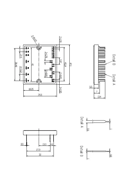
嘉兴斯达IGBT版图
- 格式:pdf
- 大小:3.72 MB
- 文档页数:51

Absolute Maximum Ratings Symbol Conditions Values UnitIGBT V CES T j = 25 °C 1200 V I C T j = 175 °CT c = 25 °C 555 A T c = 80 °C424 A I Cnom 400 A I CRM800 A V GES -20 (20)V t psc V CC = 800 V V GE ≤ 15 V V CES ≤ 1200 VT j = 150 °C8 μs T j-40 (175)°C Inverse diode V RRM T j = 25 °C 1200V I FT j = 175 °CT c = 25 °C 440A T c = 80 °C329 A I FRM 800A I FSM t p = 10 ms, sin 180°, T j = 25 °C1980A T j-40 ... 175°C Module I t(RMS)500 A T stg module without TIM-40 ... 125 °C V isolAC sinus 50 Hz, t = 1 min4000VCharacteristics Symbol Conditions min. typ. max. UnitIGBT V CE(sat)I C = 400 A V GE = 15 V chiplevel T j = 25 °C 1.55 1.85V T j = 150 °C 1.80 V V CE0chiplevel T j = 25 °C 0.84 0.90 V T j = 150 °C 0.72 V r CE V GE = 15 V chiplevelT j = 25 °C 1.78 2.4 mΩ T j = 150 °C2.7 mΩ V GE(th)V CE = 10V, I C = 40 mA5.46 6.6 V I CES V GE = 0 V, V CE = 1200 V, T j = 25 °C4.0 mA C ies V CE = 10 V V GE = 0 Vf = 1 MHz84.0 nF C oes f = 1 MHz 2.61 nF C res f = 1 MHz1.12 nF Q G V GE = - 8V ... + 15 V 4000 nC R Gint T j = 25 °C 1.5 Ω t d(on)V CC = 600 V I C = 400 AV GE =+15/-15V R G on = 1 Ω R G off = 1 Ωdi/dt on = 6000 A/µs di/dt off = 3350 A/µs T j = 150 °C 320 ns t r T j = 150 °C 66 ns E on T j = 150 °C 36 mJ t d(off)T j = 150 °C 420 ns t f T j = 150 °C 97 ns E off T j = 150 °C48mJ R th(j-c)per IGBT0.091K/W R th(c-s)per IGBT, P12 (reference) 0.038 K/W R th(c-s)per IGBT, HP-PCM0.027K/WIGBT M7 ModulesSKM400GB12M7Features*∙ V CE(sat) with positive temperature coefficient∙ High overload capability∙ Low loss high density IGBT´s ∙ Fast & soft switching inverse CAL diodes∙ Large clearance (10 mm) and creepage distances (20 mm) ∙ Insulated copper baseplate using DBC Technology (Direct Bonded Copper)∙ UL recognized, file no. E63532Typical Applications∙ AC inverter drives ∙ UPSRemarks∙ Max. case temperature limited to T C = T S = 125 °C∙Product reliability results are valid for T j = 150 °C (recommended T j,op = -40...+150 °C)∙ For storage and case temperature with TIM see document: ″Technical Explanations Thermal Interface Materials″GBSEMITRANS 3Characteristics Symbol Conditions min. typ. max. UnitInverse diode V F = V EC I F = 400 A V GE = 0 V chiplevel T j = 25 °C 2.20 2.52V T j = 150 °C 2.14 V V F0chiplevel T j = 25 °C 1.30 1.50 V T j = 150 °C 0.90 V r F chiplevelT j = 25 °C 2.3 2.6 mΩ T j = 150 °C3.1 mΩ I RRM V CC = 600 V I F = 400 AV GE = -15 Vdi/dt off = 6650 A/µs T j = 150 °C 380 A Q rr T j = 150 °C60 µC E rr T j = 150 °C 28mJ R th(j-c)per diode0.14K/W R th(c-s)per diode, P12 (reference) 0.042 K/W R th(c-s)per diode, HP-PCM0.035 K/W Module L CE 15nH R CC'+EE'measured per switchT j = 25 °C 0.55mΩ T j = 150 °C0.85 mΩ R th(c-s)1calculated without thermal coupling, P12 (reference)0.0101 K/W R th(c-s)2including thermal coupling,T s underneath module, P12 (reference)0.015 K/W R th(c-s)2including thermal coupling,T s underneath module, HP-PCM 0.0085K/W M s to heat sink M635 Nm M t to terminal M62.55 Nm -Nm w325 gSEMITRANS ® 3 IGBT M7 ModulesSKM400GB12M7Features*∙ V CE(sat) with positive temperature coefficient∙ High overload capability∙ Low loss high density IGBT´s ∙ Fast & soft switching inverse CAL diodes∙ Large clearance (10 mm) and creepage distances (20 mm) ∙ Insulated copper baseplate using DBC Technology (Direct Bonded Copper)∙ UL recognized, file no. E63532Typical Applications∙ AC inverter drives ∙ UPSRemarks∙ Max. case temperature limited to T C = T S = 125 °C∙Product reliability results are valid for T j = 150 °C (recommended T j,op = -40...+150 °C)∙ For storage and case temperature with TIM see document: ″Technical Explanations Thermal Interface Materials″GBFig. 1: Typ. output characteristic, inclusive R CC'+ EE'Fig. 2: Rated current vs. temperature I C = f (T C )Fig. 3: Typ. turn-on /-off energy = f (I C ) Fig. 4: Typ. turn-on /-off energy = f (R G )Fig. 5: Typ. transfer characteristic Fig. 6: Typ. gate charge characteristicFig. 7: Typ. switching times vs. I C Fig. 8: Typ. switching times vs. gate resistor R GFig. 9: Transient thermal impedance Fig. 10: Typ. CAL diode forward charact., incl. R CC'+ EE'Fig. 11: CAL diode peak reverse recovery current Fig. 12: Typ. CAL diode peak reverse recovery chargePinout and DimensionsGBThis is an electrostatic discharge sensitive device (ESDS) according to international standard IEC 61340.*IMPORTANT INFORMATION AND WARNINGSThe specifications of SEMIKRON products may not be considered as any guarantee or assurance of product characteristics ("Beschaffenheitsgarantie"). The specifications of SEMIKRON products describe only the usual characteristics of SEMIKRON products to be expected in typical applications, which may still vary depending on the specific application. Therefore, products must be tested for the respective application in advance. Resulting from this, application adjustments of any kind may be necessary. Any user of SEMIKRON products is responsible for the safety of their applications embedding SEMIKRON products and must take adequate safety measures to prevent the applications from causing any physical injury, fire or other problem, also if any SEMIKRON product becomes faulty. Any user is responsible for making sure that the application design and realization are compliant with all laws, regulations, norms and standards applicable to the scope of application. Unless otherwise explicitly approved by SEMIKRON in a written document signed by authorized representatives of SEMIKRON, SEMIKRON products may not be used in any applications where a failure of the product or any consequences of the use thereof can reasonably be expected to result in personal injury. No representation or warranty is given and no liability is assumed with respect to the accuracy, completeness and/or use of any information herein, including without limitation, warranties of non-infringement of intellectual property rights of any third party. SEMIKRON does not convey any license under its or a third party’s patent rights, copyrights, trade secrets or other intellectual property rights, neither does it make any representation or warranty of non-infringement of intellectual property rights of any third party which may arise from a user’s applications. Due to technical requirements our products may contain dangerous substances. For information on the types in question please contact the nearest SEMIKRON sales office. This document supersedes and replaces all previous SEMIKRON information of comparable content and scope. SEMIKRON may update and/or revise this document at any time.。