PD69104B 芯片回流焊曲线
- 格式:pdf
- 大小:231.12 KB
- 文档页数:1
回流焊PCB温度曲线讲解回流焊是一种常用的电子组装工艺,用于将电子元件焊接到印刷电路板(PCB)上。
在回流焊过程中,PCB需要经历一系列的温度变化,以确保焊点可靠连接。
下面将讲解回流焊温度曲线的各个阶段及其作用。
1. 预热阶段(Preheat Stage):回流焊过程开始时,PCB需要从室温逐渐升温至预定温度。
预热阶段的作用是除去PCB上的水分和挥发性有机物,以避免在焊接过程中产生气泡和蒸汽。
通常,预热温度为100°C至150°C,持续时间为1至2分钟。
2. 热液相预热阶段(Thermal Soak Stage):在预热阶段后,PCB会继续加热至更高的温度,通常为150°C至200°C。
这一阶段的目的是让整个PCB均匀达到焊接温度,以减少焊接过程中的热应力。
热液相预热阶段的持续时间通常为1至4分钟。
3. 焊接阶段(Reflow Stage):当PCB达到焊接温度时,焊膏开始熔化,将电子元件与PCB焊接在一起。
焊接温度通常为220°C至245°C,具体取决于焊膏的特性。
焊接阶段的持续时间通常为1至3分钟。
4. 冷却阶段(Cooling Stage):焊接完成后,PCB需要冷却到室温,以确保焊点的稳定性。
冷却阶段通常使用强制风冷却或自然冷却。
冷却时间因焊接设备和PCB的尺寸而异,一般为1至5分钟。
回流焊温度曲线中的每个阶段都有其特定的温度和时间要求,这是为了保证焊接质量和工艺稳定性。
通过控制这些参数,焊接过程中的温度变化可以最小化,从而减少因热应力引起的PCB变形和元件损坏的风险。
总结来说,回流焊温度曲线包括预热阶段、热液相预热阶段、焊接阶段和冷却阶段。
每个阶段都有其特定的温度和时间要求,以确保焊接质量和PCB的稳定性。
通过合理控制回流焊温度曲线,可以提高焊接过程的可靠性和稳定性,从而保证电子产品的性能和可靠性。
回流焊是一种广泛应用于电子制造业的关键工艺,它能够将电子元件精准地焊接到印刷电路板(PCB)上。
摘要随着半导体技术的迅速发展,电子产品的已进入各行各业,涉及航空航天、机械制造、电子商务等,可以说,我们大家的生活已无法离开电子产品。
可焊性测试是电子产品生产制造过程中检验产品可焊接性能的一种必要手段。
产品引线的焊接性能将直接影响到产品的使用,严重的焊接不良甚至会影响到整机的可靠性。
而且此类不良很多是间歇性的,有时会影响维修人员对故障的判断,造成一些不必要的损失。
本文着重介绍了各类可焊性测试方法在元器件生产中的实际应用,以及使用方法中的一些关键点。
通过在工作中的实际应用,结合标准的要点和产品的特点,在不违背标准的情况下,针对各类不同的产品,使用不同的测试方法进行检测,这样能更有效的反应产品的可焊接性能。
特别是针对一些短引脚、无引脚产品,如何使用合适的方法,甚至说使用更有说服力的润湿法来进行检测。
这些方法的研究,将有利于封装厂在生产过程中改进产品电镀品质的检测方法,能更快、更有效的发现产品的电镀缺陷,及时调整生产工艺的,提高产品质量,满足客户的需求。
关键词:可焊性;方法;标准;半导体元器件AbstractWith the rapid development of semiconductor technology, electronic products has entered into all walks of life, involved in aerospace, mechanical manufacturing, electronic commerce and so on, in other words, our life cannot leave the electronic products.Solderability test is a necessary mean to inspect the product solderability during the electronic product manufacturing process. The solderability of the lead will directly affect the product using; serious bad soldering may even affect the reliability of the machine. And such bad soldering is intermittent; sometimes it will affect maintenance personnel’s judgment for fault, causing some unnecessary loss.This article emphatically introduces the practical application of all kinds of solderability test methods in the production of components, and some key points in using the methods. Through practical application, combining the main points of the standard and the characteristics of the products, under the case of without violating the standard, for all kinds of different products, using different testing methods can reflect the solderability more effective. Especially for some short pin and no pin products, how to testby the right method or more persuasive wetting method? The research of these methods will be of conducive forpackaging factory to improve the detection method of improving products electroplating quality in the process of production, and can find plating defects of product faster and more effective to adjust the production technology, improve product quality, and meet customer demand timely.Keywords: Solderability, Methods, Standard, Semiconductor components目录目录摘要 (Ⅰ)Abstract (Ⅱ)第1章绪论 (1)1.1课题研究的目的和意义 (1)1.1.1课题背景 (1)1.1.2目的和意义 (2)1.2 国内外研究现状 (2)1.2.1 课题来源 (2)1.3 课题的主要研究内容 (4)第2章半导体元器件的可焊性描述 (6)2.1 可焊性描述 (6)2.2 测试可焊性的几种主要方法 (6)2.2.1 可焊性测试前处理 (7)2.2.2 助焊剂的使用 (9)2.2.3 焊料的使用 (10)2.2.4 槽焊法 (11)2.2.5 电烙铁法 (12)2.2.6润湿称量法 (13)2.3本章小结 (17)第3章小型短管脚产品使用润湿称量法测试 (18)3.1小型短管脚产品的定义 (18)3.2 设备介绍 (18)3.3 SOT-23产品的测试 (19)3.3.1 SOT-23封装介绍 (19)3.3.2 润湿称量法对SOT-23产品进行测试 (20)3.4本章小结 (22)第4章无外引脚产品的测试 (23)4.1 无外引脚产品介绍 (23)4.2 槽焊法测试 (24)4.3 润湿称量法测试 (25)4.4 本章小结 (26)第5章基板封装产品的测试 (27)5.1基板封装介绍 (27)5.2 槽焊法对基板封装进行测试 (27)5.3 电烙铁法进行补充测试 (29)5.4 本章小结 (29)结论 (30)江苏科技大学硕士论文参考文献 (31)致谢 (33)第1章绪论第1章绪论1.1 课题研究的目的和意义1.1.1课题背景1947年晶体管发明的同时,也开创了半导体封装的历史。
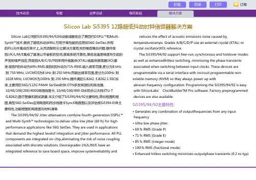
Silicon Lab公司的Si5395/94/92抖动衰减器组合了第四代DSPLL™和Multi-Synth™技术,提供了超低抖动(69fs),可用于高性能的应用如56G SerDes.所有的PLL元件集成在单片上,从而消除和分立解决方案有关的噪音耦合问题.器件级别J/K/L/M/E集成了基准以节省板的空间,提高系统可靠性,降低由温度梯度所引起的声发射噪声效应,而级别A/B/C/D/P则采用外接晶体(XTAL)或晶体振荡器(XO)基准.级别P的抖动为69fs RMS,级别E的抖动为71fs RMS.输入频率范围,差分为8 kHz 到 750 MHz, LVCMOS为8 kHz 到 250 MHz;而输出频率范围,差分为100Hz 到 1028 MHz, LVCMOS为100Hz 到 250 MHz.器件满足G.8262, E.8262.1 EEC标准.主要用在56G/112G PAM4 SerDes时钟,OTN多发探测仪和转发器,10/40/100/200/400G网络线路卡, 10/40/100/400 GbE同步以太网(ITU-TG.8262),医疗图像和测试测量.本文介绍了Si5395/94/92主要特性,简化框图和框图,典型56G SerDes应用电路和同步线路卡SyncE电路图以及评估板Si5394 EVB主要特性,功能框图和电路图与材料清单.The Si5395/94/92 Jitter attenuators combine fourth-generation DSPLL™ and Multi-Synth™ technologies to deliver ultra-low jitter (69 fs) for highperformance applications like 56G SerDes. They are used in applicationsthat demand the highest levelof integration and jitter performance. All PLL components are integrated on-chip,eliminating the risk of noise coupling associated with discrete solutions. Devicegrades J/K/L/M/E have anintegrated reference to save board space, improve systemreliability andreduces the effect of acoustic emissions noise caused bytemperatureramps. Grades A/B/C/D/P use an external crystal (XTAL) orcrystal oscillator(XO) reference.The Si5395/94/92 support free-run, synchronous and holdover modes as well as enhancedhitless switching, minimizing the phase transientsassociated when switching between input clocks. These devices areprogrammable via a serial interface with incircuit programmable non-volatile memory (NVM) so they always power up withaknown frequency configuration. Programming the Si5395/94/92 is easy with SiliconLabs’ ClockBuilderTM Pro software. Factory preprogrammed devices are also available.Si5395/94/92主要特性:• Generates any combination of outputfrequencies from any inputfrequency• Ultra low phase jitter:• 69 fs RMS (Grade P)• 71 fs RMS (Grade E)• 85 fs RMS (integer mode)• 100 fs RMS (fractional mode)• Enhanced hitless switching minimizes outputphase transients (0.2 ns typ)Silicon Lab Si5395 12路超低抖动时钟倍频器解决方案• Input frequency range• Differential: 8 kHz to 750 MHz• LVCMOS: 8 kHz to 250 MHz• Output frequency range• Differential: 100 Hz to 1028 MHz• LVCMOS: 100 Hz to 250 MHz• Meets G.8262, E.8262.1 EEC Standards• Status monitoring• Si5395: 4 input, 12 output• Si5394: 4 input, 4 output• Si5392: 4 input, 2 output• External reference: Grades A/B/C/D/P• Integrated reference: Grades J/K/L/M/E• Drop-in compatible with Si5345/44/42Si5395/94/92应用:• 56G/112G PAM4 SerDes clocking• OTN muxponders and transponders• 10/40/100/200/400G networking line cards• 10/40/100/400 GbE Synchronous Ethernet (ITU-T G.8262)• Medical imaging• Test and measurement 图1:Si5395/94/92框图图2:Si5395/94/92简化框图Si5395/94/92详细特性如下:• Generates any output frequency in any format from any inputfrequency • External XTAL or XO reference (A/B/C/D/P)• Integrated reference (J/K/L/M/E)• Ultra-low phase jitter of 69 fs (P-Grade)• Dynamic phase adjust• Input frequency range• Differential: 8 kHz–750 MHz• LVCMOS: 8 kHz–250 MHz• Output frequency range• Differential: 100 Hz to 1028 MHz• LVCMOS: 100 Hz to 250 MHz• Programmable jitter attenuation bandwidth: 0.1 Hz to 4 kHz • Meets requirements of:• ITU-T G.8262 (SyncE) EEC Options 1 and 2• ITU-T G.8262.1 (Enhanced SyncE) eEEC• Highly configurable outputs compatible with LVDS, LVPECL, LVCMOS, CML, and HCSL with programmable signal amplitude• Status monitoring (LOS, OOF, LOL)• Enhanced hitless switching for 8 kHz, 19.44 MHz, 25 MHz inputsand other frequencies• Locks to gapped clock inputs• Free-run and holdover modes• Drop-in compatible with Si5345/44/42• Optional zero delay mode• Fast-lock acquisition for low nominal bandwidths• Independent Frequency-on-the fly for each MultiSynth• DCO mode: as low as 0.001 ppb step size• Core voltage• VDD: 1.8 V ±5%• VDDA: 3.3 V ±5%• Independent output clock supply pins• 3.3 V, 2.5 V, or 1.8 V• Serial interface: I2C or SPI• In-circuit programmable with non-volatile OTP memory• ClockBuilder Pro software simplifies device configuration • Si5395: 4 input, 12 output• Grade A/B/C/D/P: 64-QFN 9×9 mm• Grade J/K/L/M/E: 64-LGA 9x9 mm• Si5394: 4 input, 4 output• Grade A/B/C/D/P: 44-QFN 7×7 mm• Grade J/K/L/M/E: 44-LGA 7x7 mm• Si5392: 4 input, 2 output• Grade A/B/C/D/P: 44-QFN 7×7 mm• Grade J/K/L/M/E: 44-LGA 7x7 mm• Temperature range: –40 to +85 ℃• Pb-free, RoHS-6 compliant图3:典型56G SerDes应用电路图4:同步线路卡SyncE电路图。
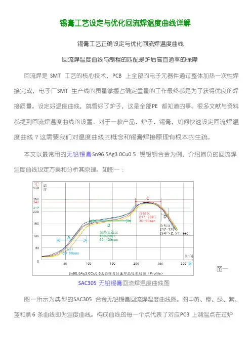
锡膏工艺设定与优化回流焊温度曲线详解锡膏工艺正确设定与优化回流焊温度曲线回流焊温度曲线与制程的匹配是炉后高直通率的保障回流焊是SMT 工艺的核心技术,PCB 上全部的电子元器件通过整体加热一次性焊接完成,电子厂SMT 生产线的质量掌握占确定重量的工作最终都是为了获得优良的焊接质量。
设定好温度曲线,就管好了炉子,这是全部PE 都知道的事。
很多文献与资料都提到回流焊温度曲线的设置。
对于一款产品、炉子、锡膏,如何快速设定回流焊温度曲线?这需要我们对温度曲线的概念和锡膏焊接原理有根本的生疏。
本文以最常用的无铅锡膏Sn96.5Ag3.0Cu0.5 锡银铜合金为例,介绍抱负的回流焊温度曲线设定方案和分析其原理。
如图一:图一SAC305 无铅锡膏回流焊温度曲线图图一所示为典型的SAC305 合金无铅锡膏回流焊温度曲线图。
图中黄、橙、绿、紫、蓝和黑6 条曲线即为温度曲线。
构成曲线的每一个点代表了对应PCB 上测温点在过炉时相应时间测得的温度。
随着时间连续的记录即时温度,把这些点连接起来,就得到了连续变化的曲线。
也可以看做PCB 上测试点的温度在炉子内随着时间变化的过程。
那么,我们把这个曲线分成4 个区域,就得到了PCB 在通过回流焊时某一个区域所经受的时间。
在这里,我们还要说明另一个概念“斜率①”。
用PCB 通过回流焊某个区域的时间除以这个时间段内温度变化确实定值,所得到的值即为“斜率”。
引入斜率的概念是为了表示PCB 受热后升温的速率,它是温度曲线中重要的工艺参数。
图中A、B、C、D 四个区段,分别为定义为A:升温区,B:预热恒温区〔保温区或活化区〕,C:回流焊接区〔焊接区或Reflow 区〕,D:冷却区。
连续深入解析个区段的设置与意义:一.升温区APCB 进入回流焊链条或网带,从室温开头受热到150℃的区域叫做升温区。
升温区的时间设置在60-90 秒,斜率掌握在2-4 之间。
此区域内PCB 板上的元器件温度相对较快的线性上升,锡膏中的低沸点溶剂开头局部挥发。
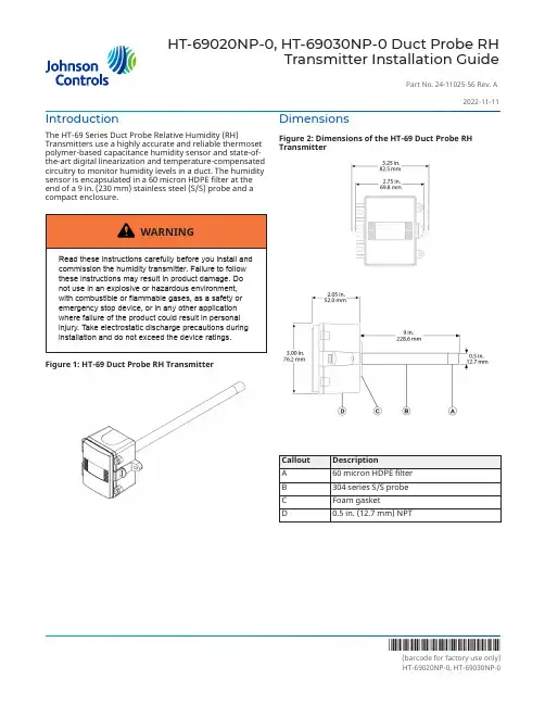
HT-69020NP-0, HT-69030NP-0 Duct Probe RHTransmitter Installation GuideIntroductionThe HT-69 Series Duct Probe Relative Humidity (RH)Transmitters use a highly accurate and reliable thermosetpolymer-based capacitance humidity sensor and state-of-the-art digital linearization and temperature-compensated circuitry to monitor humidity levels in a duct. The humidity sensor is encapsulated in a 60 micron HDPE filter at the end of a 9 in. (230 mm) stainless steel (S/S) probe and a compact enclosure.Figure 1: HT-69 Duct Probe RH Transmitter DimensionsFigure 2: Dimensions of the HT-69 Duct Probe RH Transmitter*241102556A*Part No. 24-11025-56 Rev. A2022-11-11MountingThe transmitter installs directly into any air duct with a minimum width or diameter of 10 in. (25.5 cm).-Select a suitable installation area in the middle of the duct wall.-To achieve the best reading, do not place in an area where air stratification may be present.-Mount the sensor at least 5 ft. (1.5 m) in either direction from elbows, dampers, filters, or other duct restrictions.-Avoid areas that expose the transmitter to vibrations or rapid temperature changes.To install the transmitter, complete the following steps:1.When you select a suitable spot, drill a 0.6 in. (15mm) to 0.75 in. (20 mm) hole for the probe.2.Slide the probe into the drilled hole until the enclosure is flush against the duct. The airflow direction is not important.3.Secure the enclosure to the duct with two No. 10 x 1 in. (25 mm) self-tapping screws (not provided).4.Tighten the screws until the enclosure is tight against the duct so that there is no movement of the enclosure. A foam gasket on the back of the enclosure provides a tight seal against any air leaks. See Step 1 in Figure 3.5.The enclosure includes a hinged cover with a latch.To open the cover, pull slightly on the latch on the right side of the enclosure. At the same time, pull on the cover as shown in Step 2 of Figure 3.6.A 0.5 in. NPT threaded connection hole is in the bottom of the enclosure. Screw the EMT or cable gland connector into the threaded connection holeuntil tight. See Step 3 in Figure 3.Note: Preferably use weatherproof EMT or cable gland fittings. The E-style enclosure includes 0.5 in. NPT to M16 thread adaptor and cable gland fitting.7.Make wire connections as shown in the wire diagram in Wiring .8.Swing the door closed until it securely latches. For added security, install the two provided screws in the integrated screw tabs. See Step 4 of Figure 3.Wiring•Deactivate the 24 VAC/DC power supply before you make all connections to the device to prevent electrical shock or equipment damage.•Use 14 AWG to 22 AWG shielded wiring for allconnections and do not locate the device wires in the same conduit with wiring that supplies inductive loads such as motors. Make all connections in accordance with national and local codes.•Pull at least 6 in. (15 cm) of wire into the enclosure,then complete the wiring connection according to the wire diagram for the applicable power supply and output signal type. See Figure 4.•Place the output switch in the required position to select the required signal output type (mA or VDC), as shown in Step 2 of Figure 4. The factory default setting is 4 mA to 20 mA.•If you select mA, no further output set up is required.If you select VOLT output as shown in Figure 5, place the voltage output switch to the required span position,that is 10 VDC = 0 VDC to 10 VDC. The factory default setting is 0 VDC to 10 VDC. See Step 1 of Figure 4.•Connect the DC positive or the AC voltage hot side to the PWR terminal. For voltage output or AC power,connect the supply common to the COM terminal.The device is reverse voltage-protected and does not operate if you connect it backwards. The device contains a half-wave power supply so the supplycommon is the same as the signal common. See Step 3of Figure 4.•The analog output is available on the OUT terminal.Check the controller Analog Input to determine the correct connection before you apply power as shown in Step 3 of Figure 4.Figure 3: Mounting the HT-69 Duct Probe RH TransmitterFigure 4: Wiring of the HT-60 Duct Probe TransmitterTechnical specificationsTable 1: HT-69020NP-0, HT-69030NP-0 Duct Probe RH Transmitter technical specificationsThe performance specifications are nominal and conform to acceptable industry standards. For application at conditions beyond these specifications, consult the local Johnson Controls office. Johnson Controls shall not be liable for damages resulting from misapplication or misuse of its products.Product warrantyThis product is covered by a limited warranty, details of which can be found at / buildingswarranty.Software termsUse of the software that is in (or constitutes) this product, or access to the cloud, or hosted services applicable to this product, if any, is subject to applicable end-user license, open-source software information, and other terms set forth at /techterms. Your use of this product constitutes an agreement to such terms. PatentsPatents: https://Single point of contactContact informationContact your local branch office: /locationsContact Johnson Controls: /contact-us© 2022 Johnson Controls. All rights reserved. All specifications and other information shown were current as of document revision and。
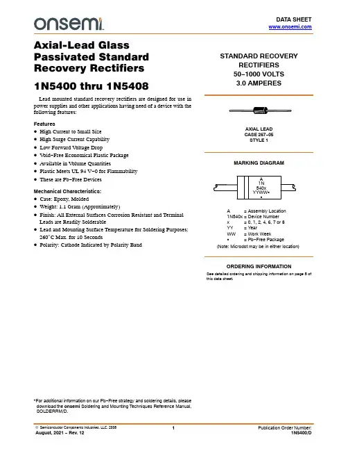
DATA SHEET Axial-Lead Glass Passivated Standard Recovery Rectifiers1N5400 thru 1N5408Lead mounted standard recovery rectifiers are designed for use in power supplies and other applications having need of a device with the following features:Features•High Current to Small Size•High Surge Current Capability•Low Forward V oltage Drop•V oid−Free Economical Plastic Package•Available in V olume Quantities•Plastic Meets UL 94 V−0 for Flammability•These are Pb−Free DevicesMechanical Characteristics:•Case: Epoxy, Molded•Weight: 1.1 Gram (Approximately)•Finish: All External Surfaces Corrosion Resistant and Terminal Leads are Readily Solderable•Lead and Mounting Surface Temperature for Soldering Purposes: 260°C Max. for 10 Seconds•Polarity: Cathode Indicated by Polarity Band*For additional information on our Pb−Free strategy and soldering details, please download the onsemi Soldering and Mounting T echniques Reference Manual, SOLDERRM/D.STANDARD RECOVERYRECTIFIERS50−1000 VOLTS3.0 AMPERESAXIAL LEADCASE 267−05STYLE 1A= Assembly Location1N540x= Device Numberx= 0, 1, 2, 4, 6, 7 or 8YY= YearWW= Work WeekG= Pb−Free PackageMARKING DIAGRAMA1N540xYYWW GGSee detailed ordering and shipping information on page 5 of this data sheet.ORDERING INFORMATION(Note: Microdot may be in either location)MAXIMUM RATINGSRating Symbol1N54001N54011N54021N54041N54061N54071N5408UnitPeak Repetitive Reverse Voltage Working Peak Reverse Voltage DC Blocking Voltage V RRMV RWMV R501002004006008001000VNon−repetitive Peak Reverse Voltage V RSM10020030052580010001200V Average Rectified Forward Current(Single Phase Resistive Load,1/2 in. Leads, T L = 105°C)I O 3.0ANon−repetitive Peak Surge Current(8 ms Single Half−Sine−Wave)I FSM200 (one cycle)AOperating and Storage Junction Temperature Range T JT stg−65 to +150−65 to +175°CStresses exceeding those listed in the Maximum Ratings table may damage the device. If any of these limits are exceeded, device functionality should not be assumed, damage may occur and reliability may be affected.THERMAL CHARACTERISTICSCharacteristic Symbol Typ Unit Thermal Resistance, Junction−to−Ambient (PC Board Mount, 1/2 in. Leads)R q JA53°C/W ELECTRICAL CHARACTERISTICSCharacteristic Symbol Min Typ Max Unit Forward Voltage (I F = 3.0 A, T A = 25°C)v F−− 1.0VReverse Current (Rated DC Voltage) T A = 25°CT A = 100°C I R−−−−1050m AProduct parametric performance is indicated in the Electrical Characteristics for the listed test conditions, unless otherwise noted. Product performance may not be indicated by the Electrical Characteristics if operated under different conditions.Ratings at 25°C ambient temperature unless otherwise specified.60 Hz resistive or inductive loads.For capacitive load, derate current by 20%.NOTE 1 — AMBIENT MOUNTING DATAFigure 1. Forward Voltagev F, INSTANTANEOUS VOLTAGE (V), I N S T A N T A N E O U S F O R W A R D C U R R E N T (A M P S )F Figure 2. Maximum Nonrepetitive Surge CurrentFigure 3. Maximum Current Derating, Lead,Various Lengthsi 40020030040NUMBER OF CYCLES5060708090100Figure 4. Maximum Current Derating, Ambient, PCBoard MountingT A, AMBIENT TEMPERATURE (°C)T L, LEAD TEMPERATURE (°C)I F S M , P E A K H A L F W A V E C U R R E N T (A )Figure 5. Forward Power Dissipation1614121086420I F(AV), AVERAGE FORWARD CURRENT (A)P F (A V ), A V E R A G E P O W E R D I S S I P A T I O N (W )I F (A V ), A V E R A G E F O R W A R D C U R R E N T (A )123456ORDERING INFORMATIONDevice Package Shipping†1N5400G Axial Lead*500 Units/Box1N5400RLG Axial Lead*1200/T ape & Reel1N5401G Axial Lead*500 Units/Box1N5401RLG Axial Lead*1200/T ape & Reel1N5402G Axial Lead*500 Units/Box1N5402RLG Axial Lead*1200/T ape & Reel1N5404G Axial Lead*500 Units/Box1N5404RLG Axial Lead*1200/T ape & Reel1N5406G Axial Lead*500 Units/Box1N5406RLG Axial Lead*1200/T ape & Reel1N5407G Axial Lead*500 Units/Box1N5407RLG Axial Lead*1200/T ape & Reel1N5408G Axial Lead*500 Units/Box1N5408RLG Axial Lead*1200/T ape & Reel†For information on tape and reel specifications, including part orientation and tape sizes, please refer to our Tape and Reel Packaging Specifications Brochure, BRD8011/D.*This package is inherently Pb−Free.SCALE 1:1CASE 267−05ISSUE G DATE 06/06/2000AXIAL LEADSTYLE 1:PIN 1.CATHODE (POLARITY BAND)2.ANODEDIM MIN MAX MIN MAXMILLIMETERSINCHESA0.2870.3747.309.50B0.1890.209 4.80 5.30D0.0470.051 1.20 1.30K 1.000---25.40---STYLE 2:NO POLARITYNOTES:1.DIMENSIONS AND TOLERANCING PER ANSIY14.5M, 1982.2.CONTROLLING DIMENSION: INCH.3.267-04 OBSOLETE, NEW STANDARD 267-05. MECHANICAL CASE OUTLINEPACKAGE DIMENSIONSON Semiconductor and are trademarks of Semiconductor Components Industries, LLC dba ON Semiconductor or its subsidiaries in the United States and/or other countries.ON Semiconductor reserves the right to make changes without further notice to any products herein. ON Semiconductor makes no warranty, representation or guarantee regarding the suitability of its products for any particular purpose, nor does ON Semiconductor assume any liability arising out of the application or use of any product or circuit, and specifically disclaims any and all liability, including without limitation special, consequential or incidental damages. ON Semiconductor does not convey any license under its patent rights nor theADDITIONAL INFORMATIONTECHNICAL PUBLICATIONS:Technical Library:/design/resources/technical−documentation onsemi Website: ONLINE SUPPORT: /supportFor additional information, please contact your local Sales Representative at /support/sales。
1. 热跑回流焊的工作原理热跑回流焊是一种常见的表面组装技术,主要用于焊接电子元件和电路板。
其工作原理是通过加热电路板上的焊膏,使其熔化并与电子元件形成焊接,然后通过冷却固化焊膏,完成焊接过程。
热跑回流焊主要包括预热区、热评台区和冷却区三个环节,其中热评台区的温度曲线是焊接质量的关键。
2. 热跑回流焊的温度曲线热跑回流焊的温度曲线一般由上升段、保持段和冷却段组成。
在上升段,焊接区域的温度逐渐升高,使焊膏熔化并与元件形成焊接。
在保持段,保持一定的温度和时间以确保焊接的牢固性和质量。
在冷却段,温度逐渐下降,焊膏固化,完成焊接过程。
3. workbench瞬态热跑回流焊温度曲线workbench瞬态热跑回流焊温度曲线是根据焊接工艺和设备特点设计的,其主要特点包括快速升温、精准控温和均匀冷却。
在上升段,workbench瞬态热跑回流焊可以快速达到需要的焊接温度,提高焊接效率。
在保持段,设备可以精确控制温度和时间,确保焊接质量。
在冷却段,设备能够实现均匀冷却,避免焊接区域温差过大,保障焊接质量。
4. workbench瞬态热跑回流焊的优势相比传统的热跑回流焊设备,workbench瞬态热跑回流焊具有以下优势:快速升温:节约生产时间,提高生产效率;精准控温:确保焊接质量,降低不良率;均匀冷却:避免焊接区域温差过大,提高焊接质量;节能环保:采用先进的节能技术,减少能源消耗,符合环保要求。
5. workbench瞬态热跑回流焊在电子制造中的应用由于其快速、精准和均匀的特点,workbench瞬态热跑回流焊在电子制造领域得到了广泛应用。
不仅可以用于焊接传统的电子元件和电路板,还可以应用于焊接更小尺寸、更复杂结构的微电子器件和柔性电子产品等新型电子制品。
在当前电子制造行业竞争激烈的环境下,workbench瞬态热跑回流焊的应用为企业提供了一种高效、可靠的焊接解决方案,有力地促进了电子制品的生产和质量提升。
6. 结语作为一种先进的电子制造技术,瞬态热跑回流焊在提高焊接效率、保障焊接质量和降低能源消耗等方面具有明显优势。
REV.AInformation furnished by Analog Devices is believed to be accurate and reliable. However, no responsibility is assumed by Analog Devices for its use, nor for any infringements of patents or other rights of third parties which may result from its use. No license is granted by implication or otherwise under any patent or patent rights of Analog Devices.aMicroprocessor Supervisory Circuits ADM690–ADM695FEATURESSuperior Upgrade for MAX690–MAX695Specified Over TemperatureLow Power Consumption (5 mW)Precision Voltage MonitorReset Assertion Down to 1 V V CCLow Switch On-Resistance 1.5 ⍀ Normal,20 ⍀ in BackupHigh Current Drive (100 mA)Watchdog Timer—100 ms, 1.6 s, or Adjustable 600 nA Standby CurrentAutomatic Battery Backup Power SwitchingExtremely Fast Gating of Chip Enable Signals (5 ns)Voltage Monitor for Power Fail APPLICATIONSMicroprocessor Systems Computers ControllersIntelligent Instruments Automotive Systems GENERAL DESCRIPTIONThe ADM690–ADM695 family of supervisory circuits offers complete single chip solutions for power supply monitoring and battery control functions in microprocessor systems. Thesefunctions include µP reset, backup battery switchover, watchdog timer, CMOS RAM write protection, and power failure warn-ing. The complete family provides a variety of configurations to satisfy most microprocessor system requirements.The ADM690, ADM692 and ADM694 are available in 8-pin DIP packages and provide:1.Power-on reset output during power-up, power-down and brownout conditions. The RESET output remains opera-tional with V CC as low as 1 V.2.Battery backup switching for CMOS RAM, CMOS microprocessor or other low power logic.3.A reset pulse if the optional watchdog timer has not been toggled within a specified time.4.A 1.3 V threshold detector for power fail warning, low battery detection, or to monitor a power supply other than +5 V.The ADM691, ADM693 and ADM695 are available in 16-pin DIP and small outline packages and provide three additional functions.1.Write protection of CMOS RAM or EEPROM.2.Adjustable reset and watchdog timeout periods.3.Separate watchdog timeout, backup battery switchover, and low V CC status outputs.The ADM690–ADM695 family is fabricated using an advanced epitaxial CMOS process combining low power consumption (5 mW), extremely fast Chip Enable gating (5 ns) and high reli-ability. RESET assertion is guaranteed with V CC as low as 1 V.In addition, the power switching circuitry is designed for mini-mal voltage drop thereby permitting increased output current drive of up to 100 mA without the need for an external pass transistor.FUNCTIONAL BLOCK DIAGRAMSV BATTV CC WATCHDOG POWER FAIL INPUT (PFI)OSC IN OSC SELCE INV BATT V CCWATCHDOG INPUT (WDI)POWER FAIL INPUT (PFI)POWER FAIL © Analog Devices, Inc., 1996One Technology Way, P.O. Box 9106, Norwood, MA 02062-9106, U.S.A.Tel: 617/329-4700Fax: 617/326-8703ADM690–ADM695–SPECIFICATIONSParameterMinTypMaxUnitsTest Conditions/CommentsBATTERY BACKUP SWITCHING V CC Operating Voltage RangeADM690, ADM691, ADM694, ADM695 4.75 5.5V ADM692, ADM6934.55.5V V BATT Operating Voltage RangeADM690, ADM691, ADM694, ADM695 2.0 4.25V ADM692, ADM693 2.04.0V V OUT Output Voltage V CC – 0.05V CC – 0.025V I OUT = 1 mA V CC – 0.5V CC – 0.25V I OUT ≤ 100 mAV OUT in Battery Backup Mode V BATT – 0.05V BATT – 0.02V I OUT = 250 µA, V CC < V BATT – 0.2 V Supply Current (Excludes I OUT )1 1.95mA I OUT = 100 mASupply Current in Battery Backup Mode 0.61µA V CC = 0 V, V BATT = 2.8 V Battery Standby Current5.5 V > V CC > V BATT + 0.2 V (+ = Discharge, – = Charge)–0.1+0.02µA T A = +25°C –1.0+0.02µA Battery Switchover Threshold 70mV Power Up V CC – V BATT50mV Power DownBattery Switchover Hysteresis 20mV BATT ON Output Voltage0.3V I SINK = 3.2 mABATT ON Output Short Circuit Current35mA BATT ON = V OUT = 4.5 V Sink Current 0.5125µABATT ON = 0 V Source CurrentRESET AND WATCHDOG TIMER Reset Voltage ThresholdADM690, ADM691, ADM694, ADM695 4.5 4.65 4.73V ADM692, ADM693 4.254.4 4.48V Reset Threshold Hysteresis 40mV Reset Timeout DelayADM690, ADM691, ADM692, ADM693355070ms OSC SEL = HIGH, V CC = 5 V, T A = +25°C ADM694, ADM695140200280ms OSC SEL = HIGH, V CC = 5 V, T A = +25°C Watchdog Timeout Period, Internal Oscillator 1.0 1.6 2.25s Long Period, V CC = 5 V, T A = +25°C 70100140ms Short Period, V CC = 5 V, T A = +25°C Watchdog Timeout Period, External Clock 38404097Cycles Long Period 7681025Cycles Short PeriodMinimum WDI Input Pulse Width 50ns V IL = 0.4, V IH = 3.5 V RESET Output Voltage @ V CC = +1 V 4200mV I SINK = 10 µA, V CC = 1 V RESET , LOW LINE Output Voltage 0.4V I SINK = 1.6 mA, V CC = 4.25 V 3.5V I SOURCE = 1 µA, V CC = 5 V RESET , WDO Output Voltage 0.4V I SINK = 1.6 mA, V CC = 5 V 3.5V I SOURCE = 1 µA, V CC = 4.25 V Output Short Circuit Source Current 1325µA Output Short Circuit Sink Current 25mA WDI Input Threshold V CC = 5 V 1Logic Low 0.8V Logic High3.5V WDI Input Current 2050µA WDI = V OUT , T A = +25°C –50–15µA WDI = 0 V, T A = +25°C POWER FAIL DETECTOR PFI Input Threshold 1.25 1.3 1.35V V CC = +5 VPFI Input Current –25±0.01+25nA PFO Output Voltage 0.4V I SINK = 3.2 mA 3.5V I SOURCE = 1 µAPFO Short Circuit Source Current 1325µA PFI = Low, PFO = 0 V PFO Short Circuit Sink Current 25mA PFI = High, PFO = V OUT CHIP ENABLE GATING CE IN Threshold0.8V V IL 3.0V V IHCE IN Pull-Up Current 3µA CE OUT Output Voltage0.4V I SINK = 3.2 mA V OUT – 1.5V I SOURCE = 3.0 mAV OUT – 0.05V I SOURCE = 1 µA, V CC = 0 VCE Propagation Delay59nsREV. A(V CC = Full Operating Range, V BATT = +2.8 V, T A = T MIN to T MAX unless otherwise noted)–2–ParameterMinTyp MaxUnits Test Conditions/CommentsOSCILLATOROSC IN Input Current±2µA OSC SEL Input Pull-Up Current 5µA OSC IN Frequency Range250kHz OSC SEL = 0 VOSC IN Frequency with External Capacitor4kHzOSC SEL = 0 V, C OSC = 47 pFNOTE 1WDI is a three level input which is internally biased to 38% of V CC and has an input impedance of approximately 125 k Ω.Specifications subject to change without notice.ADM690–ADM695REV. A –3–ABSOLUTE MAXIMUM RATINGS*(T A = +25°C unless otherwise noted)V CC . . . . . . . . . . . . . . . . . . . . . . . . . . . . . . . . . .–0.3 V to +6 V V BATT . . . . . . . . . . . . . . . . . . . . . . . . . . . . . . . .–0.3 V to +6 V All Other Inputs . . . . . . . . . . . . . . . . . .–0.3 V to V OUT + 0.5 V Input CurrentV CC . . . . . . . . . . . . . . . . . . . . . . . . . . . . . . . . . . . . .200 mA V BATT . . . . . . . . . . . . . . . . . . . . . . . . . . . . . . . . . . . .50 mA GND . . . . . . . . . . . . . . . . . . . . . . . . . . . . . . . . . . . . .20 mA Digital Output Current . . . . . . . . . . . . . . . . . . . . . . . . .20 mA Power Dissipation, N-8 DIP . . . . . . . . . . . . . . . . . . . .400 mW θJA Thermal Impedance . . . . . . . . . . . . . . . . . . . . .120°C/W Power Dissipation, Q-8 DIP . . . . . . . . . . . . . . . . . . . .500 mW θJA Thermal Impedance . . . . . . . . . . . . . . . . . . . . .125°C/W Power Dissipation, N-16 DIP . . . . . . . . . . . . . . . . . . .600 mW θJA Thermal Impedance . . . . . . . . . . . . . . . . . . . . .135°C/W Power Dissipation, Q-16 DIP . . . . . . . . . . . . . . . . . . .600 mW θJA Thermal Impedance . . . . . . . . . . . . . . . . . . . . .100°C/W Power Dissipation, R-16 SOIC . . . . . . . . . . . . . . . . . .600 mW θJA Thermal Impedance . . . . . . . . . . . . . . . . . . . . .110°C/W Operating Temperature RangeIndustrial (A Version) . . . . . . . . . . . . . . . . .–40°C to +85°C Extended (S Version) . . . . . . . . . . . . . . . . .–55°C to +125°C Lead Temperature (Soldering, 10 secs) . . . . . . . . . . . .+300°C Vapor Phase (60 secs) . . . . . . . . . . . . . . . . . . . . . . .+215°C Infrared (15 secs) . . . . . . . . . . . . . . . . . . . . . . . . . . .+220°C Storage Temperature Range . . . . . . . . . . . . .–65°C to +150°C*Stresses above those listed under “Absolute Maximum Ratings” may cause permanent damage to the device. This is a stress rating only and functional operation of the device at these or any other conditions above those listed in the operational sections of this specification is not implied. Exposure to absolute maximum ratings for extended periods of time may affect device reliability.ORDERING GUIDEModelTemperature RangePackage OptionADM690AN –40°C to +85°C N-8ADM690AQ –40°C to +85°C Q-8ADM690SQ –55°C to +125°C Q-8ADM691AN –40°C to +85°C N-16ADM691AR –40°C to +85°C R-16ADM691AQ –40°C to +85°C Q-16ADM691SQ –55°C to +125°C Q-16ADM692AN –40°C to +85°C N-8ADM692AQ –40°C to +85°C Q-8ADM692SQ –55°C to +125°C Q-8ADM693AN –40°C to +85°C N-16ADM693AR –40°C to +85°C R-16ADM693AQ –40°C to +85°C Q-16ADM693SQ –55°C to +125°C Q-16ADM694AN –40°C to +85°C N-8ADM694AQ –40°C to +85°C Q-8ADM694SQ –55°C to +125°C Q-8ADM695AN –40°C to +85°C N-16ADM695AR –40°C to +85°C R-16ADM695AQ –40°C to +85°C Q-16ADM695SQ–55°C to +125°CQ-16CAUTIONESD (electrostatic discharge) sensitive device. Electrostatic charges as high as 4000V readily accumulate on the human body and test equipment and can discharge without detection.Although the ADM690–ADM695 features proprietary ESD protection circuitry, permanent damage may occur on devices subjected to high energy electrostatic discharges. Therefore,proper ESD precautions are recommended to avoid performance degradation or loss of functionality.ADM690–ADM695REV. A–4–PIN FUNCTION DESCRIPTIONMnemonicFunctionV CC Power Supply Input: +5 V Nominal.V BATT Backup Battery Input. Connect to Ground if a backup battery is not used.V OUT Output Voltage, V CC or V BATT is internally switched to V OUT depending on which is at the highest potential. V OUT can supply up to 100 mA to power CMOS RAM. Connect V OUT to V CC if V OUT and V BATT are not used.GND 0 V. Ground reference for all signals.RESETLogic Output. RESET goes low if 1. V CC falls below the Reset Threshold 2. V CC falls below V BATT3. The watchdog timer is not serviced within its timeout period.The reset threshold is typically 4.65 V for the ADM690/ADM691/ADM694/ADM695 and 4.4 V for the ADM692 and ADM693. RESET remains low for 50 ms (ADM690/ADM691/ADM692/ADM693) or 200 ms (ADM694/ADM695)after V CC returns above the threshold. RESET also goes low for 50 (200) ms if the watchdog timer is enabled but not serviced within its timeout period. The RESET pulse width can be adjusted on the ADM691/ADM693/ADM695 as shown in Table I. The RESET output has an internal 3 µA pull up, and can either connect to an open collector Reset bus or directly drive a CMOS gate without an external pull-up resistor.WDIWatchdog Input. WDI is a three level input. If WDI remains either high or low for longer than the watchdog timeout period, RESET pulses low and WDO goes low. The timer resets with each transition on the WDI line. The watchdog timer may be disabled if WDI is left floating or is driven to midsupply.PFI Power Fail Input. PFI is the noninverting input to the Power Fail Comparator when PFI is less than 1.3 V, PFO goes low. Connect PFI to GND or V OUT when not used.PFO Power Fail Output. PFO is the output of the Power Fail Comparator. It goes low when PFI is less than 1.3 V. The comparator is turned off and PFO goes low when V CC is below V BATT .CE IN Logic Input. The input to the CE gating circuit. Connect to GND or V OUT if not used.CE OUT Logic Output. CE OUT is a gated version of the CE IN signal. CE OUT tracks CE IN when V CC is above the reset threshold. If V CC is below the reset threshold, CE OUT is forced high. See Figures 5 and 6.BATT ONLogic Output. BATT ON goes high when V OUT is internally switched to the V BATT input. It goes low when V OUT is internally switched to V CC . The output typically sinks 35 mA and can directly drive the base of an external PNP transistor to increase the output current above the 100 mA rating of V OUT .LOW LINE Logic Output. LOW LINE goes low when V CC falls below the reset threshold. It returns high as soon as V CC rises above the reset threshold.RESET Logic Output. RESET is an active high output. It is the inverse of RESET .OSC SELLogic Oscillator Select Input. When OSC SEL is unconnected (floating) or driven high, the internal oscillator sets the reset active time and watchdog timeout period. When OSC SEL is low, the external oscillator input, OSC IN,is enabled. OSC SEL has a 3 µA internal pull up, (see Table I).OSC INOscillator Logic Input. With OSC SEL low, OSC IN can be driven by an external clock signal or an externalcapacitor can be connected between OSC IN and GND. This sets both the reset active pulse timing and the watch-dog timeout period (see Table I and Figure 4). With OSC SEL high or floating, the internal oscillator is enabled and the reset active time is fixed at 50 ms typ. (ADM691/ADM693) or 200 ms typ (ADM695). In this mode the OSC IN pin selects between fast (100 ms) and slow (1.6 s) watchdog timeout periods. In both modes, the timeout period immediately after a reset is 1.6 s typical.WDOLogic Output. The Watchdog Output, WDO , goes low if WDI remains either high or low for longer than thewatchdog timeout period. WDO is set high by the next transition at WDI. If WDI is unconnected or at midsupply,the watchdog timer is disabled and WDO remains high. WDO also goes high when LOW LINE goes low.ADM690–ADM695REV. A–5–PIN CONFIGURATIONSPRODUCT SELECTION GUIDEPart Nominal Reset Nominal V CCNominal Watchdog Battery Backup Base Drive Chip Enable NumberTimeReset ThresholdTimeout PeriodSwitchingExt PNPSignalsADM69050 ms4.65 V 1.6 sYes No No ADM69150 ms or ADJ 4.65 V 100 ms, 1.6 s, ADJ Yes Yes Yes ADM69250 ms4.4 V 1.6 sYes No NoADM69350 ms or ADJ 4.4 V 100 ms, 1.6 s, ADJ Yes Yes Yes ADM694200 ms4.65 V 1.6 sYes No No ADM695200 ms or ADJ 4.65 V 100 ms, 1.6 s, ADJ Yes Yes YesCIRCUIT INFORMATION Battery Switchover SectionThe battery switchover circuit compares V CC to the V BATT input, and connects V OUT to whichever is higher. Switchover occurs when V CC is 50 mV higher than V BATT as V CC falls, and when V CC is 70 mV greater than V BATT as V CC rises. This 20 mV of hysteresis prevents repeated rapid switching if V CC falls very slowly or remains nearly equal to the battery voltage.Figure 1.Battery Switchover SchematicDuring normal operation with V CC higher than V BATT , V CC is in-ternally switched to V OUT via an internal PMOS transistorswitch. This switch has a typical on-resistance of 1.5 Ω and can supply up to 100 mA at the V OUT terminal. V OUT is normally used to drive a RAM memory bank which may require instanta-neous currents of greater than 100 mA. If this is the case then a bypass capacitor should be connected to V OUT . The capacitor will provide the peak current transients to the RAM. A capaci-tance value of 0.1µF or greater may be used.If the continuous output current requirement at V OUT exceeds 100 mA or if a lower V CC –V OUT voltage differential is desired,an external PNP pass transistor may be connected in parallel with the internal transistor. The BATT ON output (ADM691/ADM693/ADM695) can directly drive the base of the external transistor.A 20 Ω MOSFET switch connects the V BATT input to V OUT during battery backup. This MOSFET has very low input-to-output differential (dropout voltage) at the low current levels required for battery back up of CMOS RAM or other low power CMOS circuitry. The supply current in battery back up is typically 0.6 µA.The ADM690/ADM691/ADM694/ADM695 operates with battery voltages from 2.0 V to 4.25 V and the ADM692/ADM693operates with battery voltages from 2.0 V to 4.0 V. High value capacitors, either standard electrolytic or the farad size double layer capacitors, can also be used for short-term memory back up. A small charging current of typically 10 nA (0.1 µA max)flows out of the V BATT terminal. This current is useful formaintaining rechargeable batteries in a fully charged condition.This extends the life of the back up battery by compensating for its self discharge current. Also note that this current poses no problem when lithium batteries are used for back up since the maximum charging current (0.1 µA) is safe for even the smallest lithium cells.If the battery-switchover section is not used, V BATT should be connected to GND and V OUT should be connected to V CC .GNDV V OUT PFIPFO WDO VRESET OSC INRESETCE IN CE OUTWDI GND V OUT PFIVCCADM690–ADM695REV. A–6–POWER FAIL RESET OUTPUTRESET is an active low output which provides a RESET signal to the Microprocessor whenever V CC is at an invalid level. When V CC falls below the reset threshold, the RESET output is forced low. The nominal reset voltage threshold is 4.65 V (ADM690/ADM691/ADM694/ADM695) or 4.4 V (ADM692/ADM693).1 = RESET TIME.V1 = RESET VOLTAGE THRESHOLD LOW V2 = RESET VOLTAGE THRESHOLD HIGH HYSTERESIS = V2–V1Figure 2.Power Fail Reset TimingOn power-up RESET will remain low for 50 ms (200 ms for ADM694 and ADM695) after V CC rises above the appropriate reset threshold. This allows time for the power supply and mi-croprocessor to stabilize. On power-down, the RESET output remains low with V CC as low as 1 V. This ensures that the microprocessor is held in a stable shutdown condition.This RESET active time is adjustable on the ADM691/ADM693/ADM695 by using an external oscillator or by connecting an external capacitor to the OSC IN pin. Refer to Table I and Figure 4.The guaranteed minimum and maximum thresholds of the ADM690/ADM691/ADM694/ADM695 are 4.5 V and 4.73 V,while the guaranteed thresholds of the ADM692/ADM693 are 4.25 V and 4.48 V. The ADM690/ADM691/ADM694/ADM695is, therefore, compatible with 5 V supplies with a +10%, –5%tolerance while the ADM692/ADM693 is compatible with 5 V ± 10% supplies. The reset threshold comparator has approxi-mately 50 mV of hysteresis. The response time of the reset volt-age comparator is less than 1 µs. If glitches are present on the V CC line which could cause spurious reset pulses, then V CC should be decoupled close to the device.In addition to RESET the ADM691/ADM693/ADM695 con-tain an active high RESET output. This is the complement of RESET and is intended for processors requiring an active high RESET signal.Watchdog Timer RESETThe watchdog timer circuit monitors the activity of the micro-processor in order to check that it is not stalled in an indefinite loop. An output line on the processor is used to toggle theWatchdog Input (WDI) line. If this line is not toggled within the selected timeout period, a RESET pulse is generated. Thenominal watchdog timeout period is preset at 1.6 seconds on the ADM690/ADM692/ADM694. The ADM691/ADM693/ADM695may be configured for either a fixed “short” 100 ms or a “long”1.6 second timeout period or for an adjustable timeout period.If the “short” period is selected, some systems may be unable to service the watchdog timer immediately after a reset, so the ADM691/ADM693/ADM695 automatically selects the “long”timeout period directly after a reset is issued. The watchdog timer is restarted at the end of reset, whether the reset was caused by lack of activity on WDI or by V CC falling below the reset threshold.The normal (short) timeout period becomes effective following the first transition of WDI after RESET has gone inactive. The watchdog timeout period restarts with each transition on the WDI pin. To ensure that the watchdog timer does not time out,either a high-to-low or low-to-high transition on the WDI pin must occur at or less than the minimum timeout period. If WDI remains permanently either high or low, reset pulses will be issued after each “long” timeout period (1.6 s). The watchdog monitor can be deactivated by floating the Watchdog Input(WDI) or by connecting it to midsupply.RESETWDOWDIt 1 = RESET TIME.t 2 = NORMAL (SHORT) WATCHDOG TIMEOUT PERIOD.t 3 = WATCHDOG TIMEOUT PERIOD IMMEDIATELY FOLLOWING A RESET.Figure 3.Watchdog Timeout Period and Reset Active TimeADM690–ADM695REV. A –7–Table I.ADM691, ADM693, ADM695 Reset Pulse Width and Watchdog Timeout SelectionsWatchdog Timeout PeriodReset Active Period ImmediatelyOSC SEL OSC INNormal After ResetADM691/ADM693ADM695LowExternal Clock Input 1024 CLKS4096 CLKS 512 CLKS2048 CLKSLowExternal Capacitor 260 ms × C/47 pF 1.04 s × C/47 pF 130 ms × C/47 pF 520 ms × C/47 pF Floating or High Low100 ms 1.6 s 50 ms 200 ms Floating or High Floating or High 1.6 s 1.6 s 50 ms 200 msNOTEWith the OSC SEL pin low, OSC IN can be driven by an external clock signal, or an external capacitor can be connected between OSC IN and GND. The nominal internal oscillator frequency is 10.24 kHz. The nominal oscillator frequency with external capacitor is: F OSC (Hz) = 184,000/C (pF).The watchdog timeout period is fixed at 1.6 seconds, and the reset pulse width is fixed at 50 ms on the ADM690/ADM692.On the ADM694 the watchdog timeout period is also 1.6 sec-onds but the reset pulse width is fixed at 200 ms. The ADM691/ADM693/ADM695 allow these times to be adjusted as shown in Table I. Figure 4 shows the various oscillator configurations which can be used to adjust the reset pulse width and watchdog timeout period.The internal oscillator is enabled when OSC SEL is high orfloating. In this mode, OSC IN selects between the 1.6 second and 100 ms watchdog timeout periods. With OSC IN connected high or floating, the 1.6 second timeout period is selected; while with it connected low, the 100 ms timeout period is selected. In either case, immediately after a reset, the timeout period is 1.6seconds. This gives the microprocessor time to reinitialize the system. If OSC IN is low, then the 100 ms watchdog period be-comes effective after the first transition of WDI. The software should be written such that the I/O port driving WDI is left in its power-up reset state until the initialization routines are com-pleted and the microprocessor is able to toggle WDI at the mini-mum watchdog timeout period of 70 ms.Watchdog Output (WDO)The Watchdog Output WDO (ADM691/ADM693/ADM695)provides a status output which goes low if the watchdog timer “times out” and remains low until set high by the next transition on the Watchdog Input. WDO is also set high when V CC goesbelow the reset threshold.Figure 4a.External Clock SourceFigure 4b.External CapacitorNCNCFigure 4c.Internal Oscillator (1.6 Second Watchdog)Figure 4d.Internal Oscillator (100 ms Watchdog)ADM690–ADM695REV. A–8–CE Gating and RAM Write Protection (ADM691/ADM693/ADM695)The ADM691/ADM693/ADM695 products include memory protection circuitry which ensures the integrity of data in mem-ory by preventing write operations when V CC is at an invalid level. There are two additional pins, CE IN and CE OUT , which may be used to control the Chip Enable or Write inputs ofCMOS RAM. When V CC is present, CE OUT is a buffered replica of CE IN , with a 5 ns propagation delay. When V CC falls below the reset voltage threshold or V BATT , an internal gate forces CE OUT high, independent of CE IN .CE OUT typically drives the CE , CS , or write input of battery backed up CMOS RAM. This ensures the integrity of the data in memory by preventing write operations when V CC is at an in-valid level. Similar protection of EEPROMs can be achieved by using the CE OUT to drive the store or write inputs.If the 5 ns typical propagation delay of CE OUT is excessive, con-nect CE IN to GND and use the resulting CE OUT to control a high speed external logic gate.CE OUTCE INPower Fail Warning ComparatorAn additional comparator is provided for early warning of failure in the microprocessor’s power supply. The Power Fail Input (PFI) is compared to an internal +1.3 V reference. The Power Fail Output (PFO ) goes low when the voltage at PFI is less than 1.3 V. Typically PFI is driven by an external voltage divider which senses either the unregulated dc input to the system’s 5 V regulator or the regulated 5 V output. The voltage divider ratio can be chosen such that the voltage at PFI falls below 1.3 V sev-eral milliseconds before the +5 V power supply falls below the reset threshold. PFO is normally used to interrupt the micropro-cessor so that data can be stored in RAM and the shut down procedure executed before power is lostPOWER FAIL OUTPUTFigure 7.Power Fail ComparatorTable II.Input and Output Status In Battery Backup ModeSignal StatusV OUT V OUT is connected to V BATT via an internal PMOS switch.RESETLogic low.RESET Logic high. The open circuit output voltage is equal to V OUT .LOW LINELogic low.BATT ON Logic high. The open circuit voltage is equal to V OUT.WDIWDI is ignored. It is internally disconnected from the internal pull-up resistor and does not source or sink current as long as its input voltage is between GND and V OUT . The input voltage does not affect supply current.WDOLogic high. The open circuit voltage is equal to V OUT .PFIThe Power Fail Comparator is turned off and has no effect on the Power Fail Output.PFO Logic low.CE INCE IN is ignored. It is internally disconnected from its internal pull-up and does not source or sink current as long as its input voltage is between GND and V OUT . The input voltage does not affect supply current.CE OUT Logic high. The open circuit voltage is equal to V OUT .OSC IN OSC IN is ignored.OSC SEL OSC SEL is ignored.1 = RESET TIME.V1 = RESET VOLTAGE THRESHOLD LOW V2 = RESET VOLTAGE THRESHOLD HIGH HYSTERESIS = V2–V1Figure 6.Chip Enable TimingTypical Performance Curves–ADM690–ADM6955.004.801004.954.85204.90806040V O U T – VI OUT – mAFigure 8.VOUT vs. I OUT Normal Operation20120401008060P F I I N P U T T H R E S H O L D – VTEMPERATURE – °CFigure 11.PFI Input Threshold vs.Temperature61.252013451.35TIME – µsFigure 14.Power Fail Comparator Response Time 2.802.7610002.792.772002.78800600400I OUT – µAV O U T –VFigure 9.V OUT vs. I OUT Battery Backup 534920120525040511008060TEMPERATURE – °CR E S E T A C T I V E T I M E – m sFigure 12.Reset Active Time vs.Temperature 6901.251.352013458050603040702010TIME – µsFigure 15.Power Fail Comparator Response TimeFigure 10.Reset Output Voltage vs.Supply Voltage4.704.62201204.684.64404.661008060TEMPERATURE – °CR E S E T V O L T A G ET H R E S H O L D – VFigure 13.Reset Voltage Threshold vs. Temperature601.81.2501.35201345 1.61.0 1.20.60.8 1.40.40.2TIME – µsFigure 16.Power Fail Comparator Response Time with Pull-Up ResistorREV. A –9–。
LED灯珠无铅回流焊接工艺曲线设定讨论了3014LED灯珠基于95.5Sn3.8Ag0.7Cu无铅焊料的回流焊工艺。
重点绘制了无铅回流焊接工艺曲线,分析了无铅回流焊工艺升温预热区、焊接区(回流区)和冷却區等各阶段所受温度的影响及其可能引起的不良后果,为LED灯珠无铅回流焊接工艺提供参考。
标签:LED灯珠;无铅回流焊;温度曲线被誉为第四代新型照明LED光源的出现,使得各种LED产品的应用越来越广泛,如LED灯、LED显示屏等。
目前,小型化LED产品的生产大多是基于传统的表面贴装技术(SMT),锡膏回流焊接是SMT关键工艺。
以锡铅(Sn-Pb)合金作为主要焊料的锡膏,因其熔融温度低、流动性、可焊性和润湿性优良等优点被广泛应用[1]。
随着人类对环境保护的关注,广泛使用的LED产品贴装也越来越趋向于无铅化。
研究[2]表明无铅回流焊接较Sn-Pb合金回流焊相比具有焊料熔点高、焊接工艺窗口小、润湿性差等缺点。
LED灯珠规格众多,目前针对其无铅回流焊接工艺的研究报道较少,文中以长方3014LED灯珠为研究对象,讨论与其适合的无铅回流焊接工艺,以获得较好焊接效果。
1 LED灯珠及无铅锡膏的选用文中选用深圳长方集团出品的长方3014LED灯珠,市面上有售。
锡膏为较成熟的无铅焊料95.5Sn3.8Ag0.7Cu[3]锡膏,Sn-Ag-Cu系[4]合金焊料熔点在217℃附近,润湿性良好,抗热疲劳性能、化学性能均能满足LED灯珠等细间距电子元件的焊接,能有效避免桥接缺陷的出现,可获得与Sn-Pb系合金相媲美的焊点力学性能。
2 3014LED灯珠无铅回流焊温度曲线的确定借鉴Sn-Pb合金回流焊的典型温度曲线,目前工业上采用较多的无铅回流焊温度曲线主要有梯形温度曲线和渐升式温度曲线[5]。
结合典型的温度曲线,针对3014LED灯珠的特点和无铅焊料95.5Sn3.8Ag0.7Cu的性能,设计了回流温度曲线,如图1所示。
图1 无铅合金95.5Sn3.8Ag0.7Cu常规温度(实际焊点温度)曲线2.1 预热区预热区又可分为3个亚区,分别为升温区、保温区和快速升温区。
PD69104 PD69104B1 and PD69104B1-F ErrataAbout this documentThis document captures all the known erratas for PD69104B1 and PD69104B1-F device versions.PD69104 Table of ContentsAbout this document (1)1.Errata for PD69104B1 and PD69104B1-F Devices (3)1.1.LED Behavior Due to Overload (OVL) or Short at Auto Mode (3)1.2.LED Behavior Due to OVL or Short while Punishment at Auto Mode (3)1.3.Host Communication (3)1.4.UART and I2C Communications (3)2.Revision History (7)The Microchip Website (8)Product Change Notification Service (8)Customer Support (8)Microchip Devices Code Protection Feature (8)Legal Notice (8)Trademarks (9)Quality Management System (10)Worldwide Sales and Service (11)1. Errata for PD69104B1 and PD69104B1-F DevicesThis section lists the errata items and available solutions.1.1 LED Behavior Due to Overload (OVL) or Short at Auto ModeDescriptionThe port LED stays ON, although ports are OFF due to disconnect. This scenario was detected at Auto Mode only.This behavior occurs:•Sometimes when two ports are connected.•Always when three or four ports are connected.The sequence that causes the issue is:1.OVL on all ports at the same time or Short on all ports at the same time.2.Remove OVL or Short back to normal load on all ports at the same time, start-up, and then disconnect theports in any order.3.After disconnecting ports, some of the LEDs will stay ON although there is no load.WorkaroundCurrently, there is no workaround for this issue.1.2 LED Behavior Due to OVL or Short while Punishment at Auto ModeDescriptionThe port LED stays ON, although port is OFF due to disconnect. This scenario was detected at Auto Mode only. This behavior occurs always:•OVL or Short on one port, then two seconds punishment timer starts and disables this port from starting up, which causes this issue.•During this punishment time, disconnect the port.•After disconnecting the port, the LED will stay ON; although there is no load.WorkaroundCurrently, there is no workaround for this issue.1.3 Host CommunicationDescription•During UART communication, the PD69104B1 device writes zeros once the host starts to transmit the packet (starting from the first bit). The PD69104B1 device must wait until the host finishes the transmission and thenstarts to transmit another packet.WorkaroundThe host must ignore any data containing 0 before receiving the header.1.4 UART and I2C CommunicationsFor UART communications, operation of registers 0x2-0x3, 0x4-0x5, 0x6-0x7, 0x8-0x9, and 0xA-0xB is reversed from operation published in the PD69104B1 - Generic Registers Map.For I2C communication, operation is as described in the PD69104B1 - Generic Registers Map.Registers Mapping and Description for UART OperationNotes: R/W Access Key:•COR - Clear on Read. Register clears when read. Writing to these registers has no effect.•R/W - Read/Write. Register can be read or written.•RO - Read Only. Register can be read-only. Writing to these registers has no effect.•SO - Set Only. Writing 1 - set the bit, Writing 0 – bit is unchanged (Data read from these registers has no effect).•/ - Bit (or Byte) default value – depends on IC I/O configuration (pull-up or pull-down).Table 1-1. Registers Mapping and Description for UART OperationRevision History 2. Revision HistoryThe Microchip WebsiteMicrochip provides online support via our website at /. This website is used to make files and information easily available to customers. Some of the content available includes:•Product Support – Data sheets and errata, application notes and sample programs, design resources, user’s guides and hardware support documents, latest software releases and archived software•General Technical Support – Frequently Asked Questions (FAQs), technical support requests, online discussion groups, Microchip design partner program member listing•Business of Microchip – Product selector and ordering guides, latest Microchip press releases, listing of seminars and events, listings of Microchip sales offices, distributors and factory representativesProduct Change Notification ServiceMicrochip’s product change notification service helps keep customers current on Microchip products. Subscribers will receive email notification whenever there are changes, updates, revisions or errata related to a specified product family or development tool of interest.To register, go to /pcn and follow the registration instructions.Customer SupportUsers of Microchip products can receive assistance through several channels:•Distributor or Representative•Local Sales Office•Embedded Solutions Engineer (ESE)•Technical SupportCustomers should contact their distributor, representative or ESE for support. Local sales offices are also available to help customers. A listing of sales offices and locations is included in this document.Technical support is available through the website at: /supportMicrochip Devices Code Protection FeatureNote the following details of the code protection feature on Microchip products:•Microchip products meet the specifications contained in their particular Microchip Data Sheet.•Microchip believes that its family of products is secure when used in the intended manner, within operating specifications, and under normal conditions.•Microchip values and aggressively protects its intellectual property rights. Attempts to breach the code protection features of Microchip product is strictly prohibited and may violate the Digital Millennium Copyright Act.•Neither Microchip nor any other semiconductor manufacturer can guarantee the security of its code. Code protection does not mean that we are guaranteeing the product is “unbreakable”. Code protection is constantly evolving. Microchip is committed to continuously improving the code protection features of our products. Legal NoticeThis publication and the information herein may be used only with Microchip products, including to design, test,and integrate Microchip products with your application. Use of this information in any other manner violates these terms. Information regarding device applications is provided only for your convenience and may be supersededby updates. It is your responsibility to ensure that your application meets with your specifications. Contact yourlocal Microchip sales office for additional support or, obtain additional support at /en-us/support/ design-help/client-support-services.THIS INFORMATION IS PROVIDED BY MICROCHIP "AS IS". MICROCHIP MAKES NO REPRESENTATIONSOR WARRANTIES OF ANY KIND WHETHER EXPRESS OR IMPLIED, WRITTEN OR ORAL, STATUTORYOR OTHERWISE, RELATED TO THE INFORMATION INCLUDING BUT NOT LIMITED TO ANY IMPLIED WARRANTIES OF NON-INFRINGEMENT, MERCHANTABILITY, AND FITNESS FOR A PARTICULAR PURPOSE, OR WARRANTIES RELATED TO ITS CONDITION, QUALITY, OR PERFORMANCE.IN NO EVENT WILL MICROCHIP BE LIABLE FOR ANY INDIRECT, SPECIAL, PUNITIVE, INCIDENTAL, OR CONSEQUENTIAL LOSS, DAMAGE, COST, OR EXPENSE OF ANY KIND WHATSOEVER RELATED TO THE INFORMATION OR ITS USE, HOWEVER CAUSED, EVEN IF MICROCHIP HAS BEEN ADVISED OF THE POSSIBILITY OR THE DAMAGES ARE FORESEEABLE. TO THE FULLEST EXTENT ALLOWED BY LAW, MICROCHIP'S TOTAL LIABILITY ON ALL CLAIMS IN ANY WAY RELATED TO THE INFORMATION OR ITS USE WILL NOT EXCEED THE AMOUNT OF FEES, IF ANY, THAT YOU HAVE PAID DIRECTLY TO MICROCHIP FOR THE INFORMATION.Use of Microchip devices in life support and/or safety applications is entirely at the buyer's risk, and the buyer agrees to defend, indemnify and hold harmless Microchip from any and all damages, claims, suits, or expenses resulting from such use. No licenses are conveyed, implicitly or otherwise, under any Microchip intellectual property rights unless otherwise stated.TrademarksThe Microchip name and logo, the Microchip logo, Adaptec, AnyRate, AVR, AVR logo, AVR Freaks, BesTime, BitCloud, CryptoMemory, CryptoRF, dsPIC, flexPWR, HELDO, IGLOO, JukeBlox, KeeLoq, Kleer, LANCheck, LinkMD, maXStylus, maXTouch, MediaLB, megaAVR, Microsemi, Microsemi logo, MOST, MOST logo, MPLAB, OptoLyzer, PIC, picoPower, PICSTART, PIC32 logo, PolarFire, Prochip Designer, QTouch, SAM-BA, SenGenuity, SpyNIC, SST, SST Logo, SuperFlash, Symmetricom, SyncServer, Tachyon, TimeSource, tinyAVR, UNI/O, Vectron, and XMEGA are registered trademarks of Microchip Technology Incorporated in the U.S.A. and other countries. AgileSwitch, APT, ClockWorks, The Embedded Control Solutions Company, EtherSynch, Flashtec, Hyper Speed Control, HyperLight Load, IntelliMOS, Libero, motorBench, mTouch, Powermite 3, Precision Edge, ProASIC, ProASIC Plus, ProASIC Plus logo, Quiet- Wire, SmartFusion, SyncWorld, Temux, TimeCesium, TimeHub, TimePictra, TimeProvider, TrueTime, WinPath, and ZL are registered trademarks of Microchip Technology Incorporated in the U.S.A.Adjacent Key Suppression, AKS, Analog-for-the-Digital Age, Any Capacitor, AnyIn, AnyOut, Augmented Switching, BlueSky, BodyCom, CodeGuard, CryptoAuthentication, CryptoAutomotive, CryptoCompanion, CryptoController, dsPICDEM, , Dynamic Average Matching, DAM, ECAN, Espresso T1S, EtherGREEN, GridTime, IdealBridge, In-Circuit Serial Programming, ICSP, INICnet, Intelligent Paralleling, Inter-Chip Connectivity, JitterBlocker, Knob-on-Display, maxCrypto, maxView, memBrain, Mindi, MiWi, MPASM, MPF, MPLAB Certified logo, MPLIB, MPLINK, MultiTRAK, NetDetach, NVM Express, NVMe, Omniscient Code Generation, PICDEM, , PICkit, PICtail, PowerSmart, PureSilicon, QMatrix, REAL ICE, Ripple Blocker, RTAX, RTG4, SAM-ICE, Serial Quad I/O, simpleMAP, SimpliPHY, SmartBuffer, SmartHLS, SMART-I.S., storClad, SQI, SuperSwitcher, SuperSwitcher II, Switchtec, SynchroPHY, Total Endurance, TSHARC, USBCheck, VariSense, VectorBlox, VeriPHY, ViewSpan, WiperLock, XpressConnect, and ZENA are trademarks of Microchip Technology Incorporated in theU.S.A. and other countries.SQTP is a service mark of Microchip Technology Incorporated in the U.S.A.The Adaptec logo, Frequency on Demand, Silicon Storage Technology, Symmcom, and Trusted Time are registered trademarks of Microchip Technology Inc. in other countries.GestIC is a registered trademark of Microchip Technology Germany II GmbH & Co. KG, a subsidiary of Microchip Technology Inc., in other countries.All other trademarks mentioned herein are property of their respective companies.© 2021, Microchip Technology Incorporated and its subsidiaries. All Rights Reserved.ISBN: 978-1-5224-9129-3Quality Management SystemFor information regarding Microchip’s Quality Management Systems, please visit /quality.Worldwide Sales and Service© 2021 Microchip Technology Inc. and its subsidiaries Errata DS80000977A-page 11。
基于PT6913非隔离高压LED驱动IC方案驱动IC简介PT6913芯片采用线性恒流控制输出电流,内部集成功率MOS,输出电流可通过外部电阻设定为10mA~60mA. PT6913最大输入电压可达 400V,采用高端驱动方式,提供 LED 开路、LED 短路保护。
在任何情况下,输入电源高出LED负载的多余电压都由PT6913承受,LED负载不会面临过压威胁,这为整体方案提供了非常高的可靠性与稳定性。
为了防止 IC过热损坏,PT6913集成温度补偿功能,当IC内部结温上升到130℃时,PT6913开始减小输出电流,当结温达到150℃时,输出电流将会减小至 0.这可避免传统过温保护方式的闪烁问题。
工作原理PT6913A/B采用线性恒流驱动技术,电路拓扑简单实用。
LED负载,芯片与整流后的电源串联连接,构成电流回路,输出电流由IC设定。
当输入电压足够高于LED负载电压时,输出电流恒定,输入电压超出LED负载电压部分由IC承受,IC最大输入电压可达400V,满足绝大多数的AC输入应用方案特点◆ 5V~400V工作电压◆ 5~60mA可设定输出电流◆ ±5%输出电流精度◆ 可多个IC并联使用,以满足较大电流输出◆ 高功率因数◆ 高效率◆ 极少的外围元件◆ 无需电解电容◆ LED开路、短路保护◆ 温度衰减功能◆ - TJ》130℃,输出电流开始减小;- TJ》150℃,输出电流减小至0温度衰减PT6913A/B集成温度衰减功能。
当IC内部结温高于130℃(典型值)时,IS引脚电压以15mV/℃的系数减小,输出电流也因此跟着减小。
当IC内部结温达到150℃时,输出电流将会减小至0.温度衰减功能可有效地避免传统过热保护功能导致的闪烁现象。
当环境温度异常导致IC结温升高并达到130℃,PT6913A/B将试图通过减小输出电流来减少LED发热量,从而降低环境温度。
输出电流与环境温度将可能达到平衡,这有别于传统过热保护机制(比如:IC结温达到150℃,IC关闭,IC结温回降20℃,IC重新工作),从而避免了LED闪烁。