热退火对多晶硅特性的影响
- 格式:pdf
- 大小:419.63 KB
- 文档页数:4
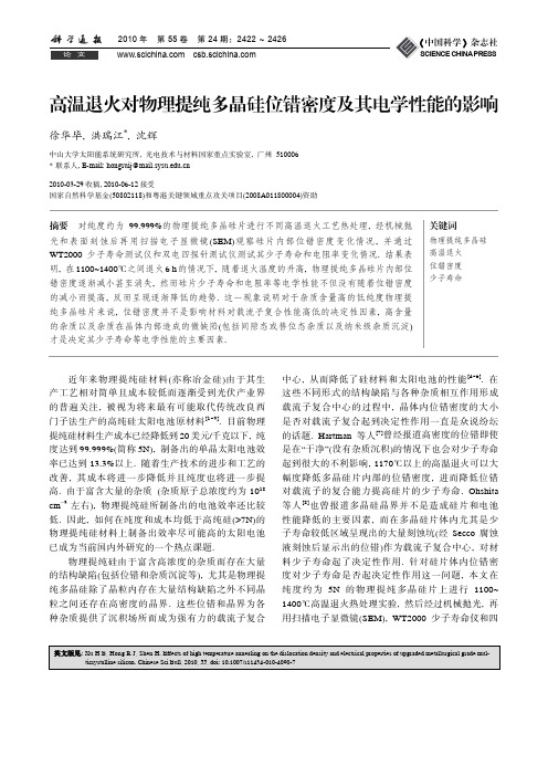
2010年 第55卷 第24期:2422 ~ 2426 英文版见: Xu H B, Hong R J, Shen H. Effects of high temperature annealing on the dislocation density and electrical properties of upgraded metallurgical grade mul-ticrystalline silicon. Chinese Sci Bull, 2010, 55, doi: 10.1007/s11434-010-4090-7论 文《中国科学》杂志社SCIENCE CHINA PRESS高温退火对物理提纯多晶硅位错密度及其电学性能的影响徐华毕, 洪瑞江*, 沈辉中山大学太阳能系统研究所, 光电技术与材料国家重点实验室, 广州 510006 * 联系人, E-mail: hongruij@ 2010-03-29收稿, 2010-06-12接受国家自然科学基金(50802118)和粤港关键领域重点攻关项目(2008A011800004)资助摘要 对纯度约为99.999%的物理提纯多晶硅片进行不同高温退火工艺热处理, 经机械抛光和表面刻蚀后再用扫描电子显微镜(SEM)观察硅片内部位错密度变化情况, 并通过WT2000少子寿命测试仪和双电四探针测试仪测试其少子寿命和电阻率变化情况. 结果表明, 在1100~1400℃之间退火6 h 的情况下, 随着退火温度的升高, 物理提纯多晶硅片内部位错密度逐渐减小甚至消失, 然而硅片少子寿命和电阻率等电学性能不但没有随着位错密度的减小而提高, 反而呈现逐渐降低的趋势. 这一现象说明对于杂质含量高的低纯度物理提纯多晶硅片来说, 位错密度并不是影响材料对载流子复合性能高低的决定性因素, 高含量的杂质以及杂质在晶体内部造成的微缺陷(包括间隙态或替位态杂质以及纳米级杂质沉淀)才是决定其少子寿命等电学性能的主要因素.关键词物理提纯多晶硅 高温退火 位错密度 少子寿命近年来物理提纯硅材料(亦称冶金硅)由于其生产工艺相对简单且成本较低而逐渐受到光伏产业界的普遍关注, 被视为将来最有可能取代传统改良西门子法生产的高纯硅太阳电池原材料[1~3]. 目前物理提纯硅材料生产成本已经降低到20美元/千克以下, 纯度达到99.999%(简称5N), 制备出的单晶太阳电池效率已达到13.3%以上. 随着生产技术的进步和工艺的改善, 其成本将进一步降低并且纯度也将进一步提高. 由于富含大量的杂质 (杂质原子总浓度约为1018 cm −3左右), 物理提纯硅所制备出的电池效率还比较低. 因此, 如何在纯度和成本均低于高纯硅(>7N)的物理提纯硅材料上制备出效率尽可能高的太阳电池已成为当前国内外研究的一个热点课题.物理提纯硅由于富含高浓度的杂质而存在大量的结构缺陷(包括位错和杂质沉淀等), 尤其是物理提纯多晶硅除了晶粒内存在大量结构缺陷之外不同晶粒之间还存在高密度的晶界. 这些位错和晶界为各种杂质提供了沉积场所而成为强有力的载流子复合中心, 从而降低了硅材料和太阳电池的性能[4~6]. 在这些不同形式的结构缺陷与各种杂质相互作用形成载流子复合中心的过程中, 晶体内位错密度的大小是否对载流子复合起到决定性作用一直是众说纷纭的话题. Hartman 等人[7]曾经报道高密度的位错即使是在“干净”(没有杂质沉积)的情况下也会对少子寿命起到很大的不利影响, 1170℃以上的高温退火可以大幅度降低多晶硅片内部的位错密度, 进而降低位错对载流子的复合能力提高硅片的少子寿命. Ohshita 等人[8]也曾报道多晶硅晶界并不是造成硅片和电池性能降低的主要因素, 而在多晶硅片体内尤其是少子寿命较低区域呈现出的大量刻蚀坑(经Secco 腐蚀液刻蚀后显示出的位错)作为载流子复合中心, 对材料少子寿命起了决定性作用. 针对硅片体内位错密度对少子寿命是否起决定性作用这一问题, 本文在纯度约为5N 的物理提纯多晶硅片上进行1100~ 1400℃高温退火热处理实验, 然后经过机械抛光, 再用扫描电子显微镜(SEM), WT2000少子寿命仪和四2423探针测试仪分别观察和测试不同退火温度下硅片体内位错密度、少子寿命和电阻率的变化情况.1 材料和方法(ⅰ) 实验材料和仪器. 本实验过程中所采用的物理提纯多晶硅片由上海普罗新能源有限公司提供, 纯度约为5N. 硅片中除碳(C)和氧(O)含量约为1017~1018 cm −3之外, 其余的硼(B)、磷(P)、铁(Fe)、铝(Al)和钙(Ca)等一些主要金属杂质质量百分比含量如表1所示(测试数据由硅片生产厂家提供). 实验中使用的主要仪器和设备有: 真空高温管式炉(GSL-1600X, 合肥科晶材料技术有限公司), SEM (EVO-LS, 德国), 少子寿命仪(WT2000, 匈牙利SE- MILAB 公司), 四探针测试仪(RTS-9, 广州四探针科技有限公司).(ⅱ) 实验方法. 为了便于对比不同温度下退火工艺对硅片位错密度和电学性能的影响, 硅片样品均选用紧邻在一起的姊妹片, 这样可以近似认为硅片在退火处理之前具有相同的物理结构、组成和性质, 包括位错密度、晶界结构、少子寿命、电阻率以及杂质含量和分布等. 选取物理提纯多晶硅相邻的姊妹片4片, 取其中1片作为对比样品(原片), 另外3片多晶分别在1160, 1260和1360℃三个温度点下采用真空高温管式炉进行退火6 h, 各退火工艺温度条件如图1所示. 高温退火过程中均采用氮气(N 2)保护, 退火后的样品和原片一起经过机械抛光清洗后再在Sirtl 腐蚀液(HF:5MCrO 3) 中刻蚀30 s 以便用SEM 观察硅片内部位错密度变化情况, 然后借助WT2000少子寿命仪测试少子寿命并用四探针测试仪测量其电阻率.2 结果和分析2.1 位错密度的变化物理提纯多晶硅片分别在1160, 1260, 1360℃, 在N 2保护的气氛下进行连续高温退火6 h, 经过不同高温退火工艺处理的硅片和原片一起采用机械抛光后再用Sirtl 腐蚀液刻蚀30 s, 之后采用SEM 观察其图1 高温退火温度条件(a) 1360℃; (b) 1160℃/1260℃位错密度变化情况. 图2则是多晶硅样品经过不同温度退火后某一具有代表性晶界处平均位错密度的统计结果, 图3则是对应温度下其表面刻蚀坑在放大2000倍后所看到的SEM 对比照片. 从图中可以看出: 3个多晶硅姊妹片分别经过不同温度退火后与原片相比, 其刻蚀坑的密度均有不同程度的降低, 且随着退火温度的升高呈逐渐减小的趋势. 特别是当退火温度达到1360℃时,硅片上除了晶界仍然清晰可见图2 物理提纯多晶硅退火后平均位错密度变化情况表1 物理提纯多晶硅片主要杂质质量百分比含量杂质 B P Fe Al Ca Cu Ni Cr Pb 含量(%)0.00032 0.0005 0.0002 0.0003 0.0002 <0.0001 <0.0001 <0.0001 <0.00012010年8月第55卷 第24期2424图3 物理提纯多晶硅片不同温度下退火后位错密度变化对比SEM 照片(放大2000倍)(a) 原片; (b) 1160℃; (c) 1260℃; (d) 1360℃之外剩下的刻蚀坑寥寥无几而接近消失. 这表明物理提纯多晶硅片经过1100~1400℃高温退火处理, 其体内位错密度随退火温度的升高而逐渐减小甚至完全消失. 这种变化趋势与Hartman 等人[7]实验结果是完全一致的.研究表明[9,10], 在超过1000℃的条件下, 硅片内晶界和位错处沉积的大量金属杂质沉淀会逐渐溶解进而扩散到晶粒内部. 一般来说, 随着温度的升高, 杂质沉淀溶解的速度加快, 相应地也会促进杂质在硅片晶粒内部的扩散. 与此同时, 随着晶界和位错处杂质沉淀逐渐溶解和扩散, 晶界和位错均会沿着滑移面发生移动现象, 尤其是硅片晶粒内部位错在600℃左右就可以在滑移面上移动[11], 当温度达到1000℃后, 晶粒内部位错就会不受滑移面限制地移动, 进而通过移动外扩到硅片表面或者通过位错之间的相互抵消而消失[12]. 如此看来, 实验中物理提纯多晶硅片体内位错密度随退火温度升高逐渐减小甚至消失的现象, 是由于原来沉积在位错和晶界处不同杂质及其沉淀在高温下溶解扩散和位错滑移共同作用的结果.2.2 电学性能的变化经过退火、抛光和刻蚀后的样品均采用WT2000少子寿命仪在裸片上测出少子寿命(如图4所示), 并采用四探针测试仪测出各样品的电阻率(如图5所示). 结果表明: 经过1100℃以上的高温退火热处理, 样品的少子寿命和电阻率相对于原片均有不同程度的降低. 从图示的曲线可以看出, 硅片样品的少子寿命和电阻率随着退火温度的升高均呈现逐渐降低的趋势.需要说明的是: 在实验前后物理提纯多晶硅片中的杂质总体含量是没有发生改变的, 发生变化的是硅片样品在高温退火后位错密度、少子寿命和电阻率均有不同程度地下降, 同时硅片内杂质的化学结构和状态及其空间分布在高温下可能会发生相应的改变. Istratov 等人[13~15]研究表明: 在同一硅片样品图4 物理提纯多晶硅退火后少子寿命变化情况图5 物理提纯多晶硅退火后电阻率变化情况上, 少子寿命高的“优区”和少子寿命低的“劣区”其杂质含量往往没有明显的区别, 当硅片中大量金属杂质沉积在晶界或者位错处形成沉淀时其复合性能较低, 而高浓度的金属杂质一旦处于间隙态或者替位态时其形成的载流子复合中心足以将少子扩散长度降低到1 μm以下. 硅片性能好坏或者电池效率的高低不仅与其材料总体杂质浓度有关, 而且还与杂质在硅片中所处的化学结构和状态以及空间分布情况有关, 例如, 铁和铜常在硅中以硅化物的形式在晶界或位错处沉积生成Fe2Si[9]和Cu3Si[16]. 此外, Buon-assisi等人[10]也曾研究表明: 在高温退火后缓慢冷却的过程中, 硅片中过渡性金属杂质形成的大量纳米级颗粒沉淀会广泛且较均匀地分布于晶粒内的微缺陷处, 这种纳米级颗粒沉淀一般是多种金属混合在一起形成的硅化物、氧化物和碳化物等, 其对载流子的复合能力比那些非均匀地沉积或聚集在晶界和位错处的微米级大尺寸沉淀要大得多, 对硅材料的电学性能起了重要的作用. 也就是说, 在硅片中大量的金属杂质既有与晶界和位错等结构缺陷结合在一起形成复合能力较低的微米级大尺寸沉淀或聚合体,又有广泛分布于晶粒内以间隙态、替位态杂质和纳米级颗粒沉淀等形式存在形成具有较强复合能力的微缺陷. 因此, 为了提高硅片性能和电池效率, 可以选择合适的退火温度将硅片中某些对硅料性能有致命影响的杂质转换成复合能力更低的状态, 比如在400~500℃下退火可以促使晶体硅片中更多的间隙态铁杂质生成沉淀, 进而降低间隙态铁对载流子的复合能力提高硅片电学性能[17].对于高杂质含量的物理提纯多晶硅而言, 金属杂质的浓度远远超过其在硅晶体中的固溶度使得大部分金属杂质不均匀地沉积在晶界或者位错处而以沉淀或聚合体形式存在, 只有约占总含量1%~10%的小部分金属杂质分散在硅晶体中以间隙态或替位态形式存在. 这一小部分处于间隙态或替位态的金属杂质由于具有较强的复合性能往往决定了载流子的扩散长度, 只要金属杂质在硅料中的化学结构和状态及其分布发生微小的变化就会引起材料复合性能的改变, 而这种载流子复合性能的改变与硅料中总体金属杂质含量无关[9]. 可以想象, 实验中物理提纯多晶硅片中高浓度杂质在晶界和位错处沉积的大尺寸微米级沉淀会在高温退火过程中逐渐溶解扩散到晶粒内部, 从而以间隙态或替位态杂质形式广泛分布于晶粒中成为载流子复合中心, 或者在晶粒内微缺陷处形成大量的纳米级颗粒沉淀也会构成强有力的载流子复合中心. 这些在高温退火下溶解扩散进而在晶粒内部造成大量均匀分布的微缺陷复合中心大大降低了硅片的少子寿命, 同时也使得原来比较“干净”的晶粒变得不再干净了, 晶粒晶格中由于大量杂质的引入尤其是金属杂质的存在使得样品少子寿命和电阻率在高温退火后均有所下降而且随着退火温度的升高呈逐渐降低的趋势.实验结果表明, 物理提纯多晶硅片的少子寿命等电学性能不但没有随着其位错密度的减小而升高反而还会降低, 这与Hartman等人[7]所报道的位错密度是决定硅料尤其是多晶硅少子复合性能的决定性因素是不完全一致的. 由此可见, 对高杂质含量的物理提纯硅来说, 特别是多晶硅, 影响其材料性能的因素不仅仅是硅片中晶界和位错密度的大小, 硅片中杂质尤其是金属杂质在硅片中的化学结构和状态及24252010年8月 第55卷 第24期2426其在硅片中的空间分布对材料的性能也是很重要的甚至起了决定性作用. 而对于杂质含量较低(>7N)的硅料来说, 晶体内部晶界和位错密度往往是决定材料对载流子复合能力高低的主要因素, 这种说法在Ehret 等人[18]对电磁浇铸(EMC)硅材料的研究中得到了应证.3 结论通过对高杂质含量低纯度的物理提纯多晶硅片进行1000~1400℃高温退火实验可知: 随着退火温度的升高, 硅片内部位错密度逐渐减小, 与此同时, 硅片少子寿命和电阻率也随之下降. 这表明对于纯度约为5N 杂质含量较高的物理提纯硅来说, 特别是多晶硅, 晶体内部位错密度并不是决定材料对载流子复合性能高低的主要因素, 决定材料复合性能高低的是高浓度杂质尤其是金属杂质在晶粒中的化学结构和状态及其在晶粒中的空间分布情况. 因此, 在物理提纯硅片制备成太阳能电池的过程中, 采用合适的温度进行退火处理, 以期将某些有害杂质转化成复合性能更低的化学结构和状态是尤为必要的.参考文献1 Gribov B G, Zinov’ev K V. Preparation of high-purity silicon for solar cells. Inorg Mater, 2003, 39: 653—6622 Müller A, Ghosh M, Sonnenschein R, et al. Silicon for photovoltaic applications. Mater Sci Eng B, 2006, 134: 257—2623 Bathey B R, Cretealla M C. Review: Solar-grade silicon. J Mater Sci, 1982, 17: 3077—30964 Binetti S, Libal J, Acciarri M, et al . Study of defects and impurities in multicrystalline silicon grown from metallurgical silicon feedstock.Mater Sci Eng B, 2009, 159-160: 274—2775 Taishi T, Hoshikawa T, Yamatani M, et al. Influence of crystalline defects in Czochralski-grown Si multicrystal on minority carrier life-time. J Cryst Growth, 2007, 306: 452—4576 Sopori B, Chen W, Tan T, et al. Overcoming the efficiency-limiting mechanisms in commercial Si solar cells. NCPV Photovolt ProgramRev, 1999: 341—3477 Hartman K, Bertoni M, Serdy J, et al. Dislocation density reduction in multicrystalline silicon solar cell material by high temperature an-nealing. Appl Phys Lett, 2008, 93: 1221088 Ohshita Y, Nishikawa Y, Tachibana M, et al. Effects of defects and impurities on minority carrier lifetime in cast-grown polycrystallinesilicon. J Cryst Growth, 2005, 275: e491—e4949 Buonassisi T, Istratov A A, Peters S, et al. Impact of metal silicide precipitate dissolution during rapid thermal processing of multicrys-talline silicon solar cells. Appl Phys Lett, 2005, 87: 12191810 Buonassisi T, Heuer M, Istratov A A, et al. Transition metal co-precipitation mechanisms in silicon. Acta Mater, 2007, 55: 6119—6126 11 Gumbsch P, Riedle J, Hartmaier A, et al. Controlling factors for the Brittle-to-ductile transition in tungsten single crystals. Science, 1998,282: 1293—129512 Takeuchi S, Argon A S. Review: Steady-state creep of single-phase crystalline matter at high temperature. J Mater Sci, 1976, 11: 1542—156613 Istratov A A, Buonassisi T, McDonald R J, et al, Metal content of multicrystalline silicon for solar cells and its impact on minority carrierdiffusion length. J Appl Phys, 2003, 94: 6552—655914 Buonassisi T, Istratov A A, Pickett M D, et al. Chemical nature and distributions of metal impurities in multicrystalline silicon materials.Prog Photovolt: Res Appl, 2006, 14: 513—53115 Buonassisi T, Istratov A A, Heuer M, et al. Synchrotron-based investigations of the nature and impact of iron contamination in multicrys-talline silicon solar cells. J Appl Phys, 2005, 97: 07490116 Buonassisi T, Marcus M A, Istratov A A, et al. Analysis of copper-rich precipitates in silicon chemical state, gettering, and impact onmulticrystalline silicon solar cell material. J Appl Phys, 2005, 97: 06350317 Pickett M D, Buonassisi T. Iron point defect reduction in multicrystalline silicon solar cells. Appl Phys Lett, 2008, 92: 12210318 Ehret E, Marty O. Correlation between electrical activity and extended defect in EMC multicrystalline materials. Mater Sci Eng B, 1998,56: 24—30。

引言快速光热退火是近年来制备多晶硅薄膜过程中的一种新兴工艺[1-2],它克服了传统高温炉生长法用时长,成本高,结晶质量较差的问题[3-4]。
卤钨灯的光照因素是影响结晶质量的关键参数,所以研究光波频率与光照强度对多晶硅薄膜的影响,是改进发展光热退火法的一个重要研究方向。
1 实验我们制备a-Si:H薄膜样品制备采用四室沉积设备,射频频率13.6MHz,工作气体是SiH4+H2混合气体,其中SiH4气体混合比为1:5,压强150Pa,射频功率80W,沉积时基片预加热至200℃,沉积时间为2h,制备好的非晶硅薄膜经台阶测厚仪测定,厚度约为1000nm。
将制备好的a-Si:H薄膜进行快速退火,用 12个卤钨灯 (上下各6个)作为光热退火的光源,高纯氮气保护压力为1个大气压。
一组为光热退火(12个灯,温度700℃)与不退火样品的对比;一组为采用相同数量卤钨灯照射,但退火温度不同;一组为采用相同升温速度和退火温度,但卤钨灯数量不同的比较,使用的电压也不同,以发现变化规律,研究作用机理。
2 结果与分析图1是a-Si:H薄膜退火前后的XRD图,A图为薄膜退火前XRD,散射峰在480cm-1附近,它对应非晶硅的散射峰,退火前薄膜a-Si:H薄膜。
退火后散射峰在510cm-1附近,形状窄而锐,表示薄膜已经具有明显晶相结构。
光照因素在光热退火法制备多晶硅中的影响分析魏晋军 西北师范大学知行学院,甘肃兰州 730070马书懿 西北师范大学物电学院DOI:10.3969/j.issn.1001-8972.2011.16.032图1 样品退火前后的XRD谱图图2 样品相同温度不同光强照退火的XRD谱图图2是a-Si:H薄膜采用相同的退火温度,但采用不同数量的卤钨灯照射样品的XRD谱图,在28°都有较强的衍射峰,说明择优取向仍为(111)晶向,用10盏卤钨灯照射样品的(111)晶向峰要比12盏卤钨灯照射样品的要强,说明使用10盏灯照射的晶化效果要好,由于它们升温的速度和退火的速度是一样的,而10V卤钨灯照射时,为了达到相同的升温速度,必须加大电源电压,导致卤钨灯发射的光子比较多。

第26卷 第12期2005年12月半 导 体 学 报CHIN ESE J OURNAL OF SEMICONDUCTORSVol.26 No.12Dec.,2005Received 10J une 2005 Ζ2005Chinese Institute of ElectronicsE ffect of Therm al Annealing on Characteristicsof Polycrystalline SiliconRen Bingyan 1,Gou Xianfang 1,2,Ma Lifen 1,2,Li Xudong 2,Xu Ying 2,and Wang Wenjing 2(1Semiconductor Research I nstit ute ,Hebei Uni versit y of Technolog y ,Tianj in 300130,China )(2B ei j ing S olar Energ y Research I nstit ute ,Bei j i ng 100083,China )Abstract :Oxygen and carbon behaviors and minority 2carrier lifetimes in multi 2crystalline silicon (mc 2Si )used for solar cells are investigated by FTIR and QSSPCD before and after annealing at 750~1150℃in N 2and O 2ambient.For comparison ,the annealing of CZ silicon with nearly the same oxygen and carbon concentrations is also carried out under the same conditions.The results reveal that the oxygen and carbon concentrations of mc 2Si and CZ 2Si have a lesser decrease ,which means oxygen precipitates are not generated ,and grain boundaries in mc 2Si do not affect car 2bon behavior.Bulk lifetime of mc 2Si increases in N 2and O 2ambient at 850,950,and 1150℃,and the lifetime of mc 2Si wafers annealed in O 2are higher than those annealed in N 2,which shows that a lot of impurities in mc 2Si at high temperature annealing diff use to grain boundaries ,greatly reducing recombination centers.Interstitial Si atoms filling vacancies or recombination centers increases lifetime.K ey w ords :polycrystalline silicon ;oxygen ;lifetime EEACC :2520CC LC number :TN30411+2 Document code :A Article ID :025324177(2005)12222942041 IntroductionPolycrystalline Si wafers have become preva 2lent in t he recent p hotovoltaic market.However ,t hey need f urt her quality imp rovement for highly efficient ,low 2co st solar cells.First we must under 2stand t he behaviors of imp urities and defect s in t he polycrystalline Si wafers in more detail.Because t here are grain boundaries and more imp urities and defect s ,mc 2Si material has more complicated p hysi 2cal behavior in high temperat ure annealing t han mono 2crystalline silicon.Oxygen in mc 2Si is a very important imp urity t hat affect s t he elect rical and mechanical properties of silicon material during heat t reat ment s [1].However ,t he formation of oxy 2gen precipitates ,t he variety of minor carrier life 2times ,and t he influence of t he annealing ambient are less investigated for polycrystalline silico n solarcells.In t his paper ,t he effect s of t hermal annealingon oxygen behavior and carrier lifetimes for poly 2crystalline Si wafers are investigated.2 ExperimentThe polycrystalline Si wafers provided by Ba 2yer Solar Corporation in t his experiment were p 2type ,019Ω・cm ,and 285μm t hick.The interstitial oxygen and substit ute carbon concent rations of t he samples were 813×1017and 2×1017cm -3,respec 2tively.For comparison ,p 2type CZ 2Si samples wit h〈100〉orientation ,1~3Ω・cm ,a t hickness of330μm ,and almost t he same oxygen concent ration were also st udied.The samples were cleaned wit h chemical solution ,and Si oxide was removed in an HF (10%)solution.Then t hey were subjected to heat t reat ment at 1260℃for 1h in N 2ambient so as to eliminate t he influence of t hermal history before第12期Ren Bingyan et al.: Effect of Thermal Annealing on Characteristics of Polycrystalline Siliconannealing [2].A single step heat t reat ment was t hen carried out in t he temperat ure range of 750~1150℃for 4h in N 2and O 2ambient.Interstitial ox 2ygen concent rations and minority 2carrier lifetimes before and after annealing were determined by F T 2IR (Fourier transmission inf rared spect ro scopy )and QSSPCD (quasi 2steady state p hotoconductance decay ).Finally ,t he samples were etched by Sirtl or Wright solution and were examined wit h an optical microscope and SEM.3 R esults3.1 Change of the interstitial oxygen concentra 2tions Figures 1and 2show t he profiles of t he inter 2stitial oxygen co ncent ration of CZ 2Si and mc 2Si during single step annealing in t he temperat ure range of 750~1150℃in N 2and O 2ambient.It can be seen t hat t he oxygen concent ration in CZ 2Si and mc 2Si slightly decreases (except for t he light in 2crease in mc 2Si at 950℃).The change of oxygen concentration is almo st uniform in N 2and O 2an 2nealing.This indicates t hat t here is almost no gen 2eration of oxygen p recipitates in CZ 2Si and mc 2Si wafers in N 2or O 2ambient.This has less influence on oxygen concent ration during single step annea 2ling.Fig.1 Interstitial oxygen changes with annealing tem 2perature under N 2and O 2surrounding in CZ 2SiwafersFig.2 Interstitial oxygen changes with annealing tem 2perature under N 2and O 2surrounding in mc 2Si wafers3.2 Change of substitute carbon concentration Carbon in CZ silicon has been reported to have a significant influence on oxygen precipitation dur 2ing heat t reat ment s.In addition ,t here is a much higher carbon concent ration in mc 2Si t han in CZ silicon.Carbon can enhance t he nucleation of oxy 2gen precipitates at low temperatures (<850℃)and does not affect t he amount of oxygen precipitatesat higher temperat ures (>950℃)[2].Carbon con 2centration after annealing was determined by F T 2IR.As shown in Table 1,t he carbon concent ration does not affect t he amount of oxygen precipitate at higher temperat ures in single annealing ,and grain bo undaries in mc 2Si do not affect carbon behavior.Table 1 Change of substitute carbon concentration of mc 2SiT /℃75085095010501150[C s ]/1017cm -3N 2ambient 2.051.92.152.21.6[C s ]/1017cm -3O 2ambient2.4 2.6 2.5 1.8 2.63.3 Change of carrier lifetimeFigures 3and 4show change of carrier lifetimeof silicon wafers during single step annealing in t he temperat ure range of 750~1150℃in N 2and O 2ambient.The lifetime of CZ 2Si wafers after annea 2ling decreases drastically wit h increasing annealing5922半 导 体 学 报第26卷temperat ure but has a recovery at 950℃,which p robably generates many defect s and new recombi 2nation centers ,and some interstitial Si atoms filling vacancies or recombination centers result in life 2time recovery at 950℃.Also ,t he lifetime of CZ 2Si wafers annealed in O 2ambient is lower t han t hose annealed in N 2.This p henomenon is probably due to t he fact t hat during annealing in O 2ambient ,in 2terstitial Si atoms are supplied from a growing SiO 2/Si interface so t hat excess interstitial Si at 2oms might recreate new recombination centers [3].Fig.3 Ratio of minority carrier lifetime changes with annealing temperature under N 2and O 2surrounding in CZ 2SiwafersFig.4 Ratio of minority carrier lifetime changes with annealing temperature under N 2and O 2surrounding in mc 2Si wafersAs shown in Fig.4,t he lifetime of minority carriers in mc 2Si wafers has great increases at 850,950,and 1150℃,respectively.The changes of life 2time in N 2and O 2ambient are almo st t he same.The lifetime of mc 2Si wafers annealing at 1150℃increases 120%in O 2ambient and t he lifetime of mc 2Si wafers annealed in O 2ambient is higher t han t hose annealed in N 2.The reason for t he increase is p robably due to t he fact t hat a lot of imp urities in mc 2Si at high temperat ure annealing diff use to grain boundaries ,greatly reducing recombination centers.On t he ot her hand ,interstitial Si atoms filling vacancies or recombination centers result s in a lifetimeincrease.Fig.5 SEM (500×)(a )and optical micrographs (200×)(b )of defects in the cleavage plane of mc 2Si after annealing at 1050℃4 ConclusionWe conclude t hat t he oxygen concentration of mc 2Si and CZ 2Si had a slight decrease (except for a light increase in mc 2Si at 950℃)in N 2and O 2am 2bient during single 2step annealing ,which means oxygen precipitates were generated.Lower carbon concent ration did not affect t he amount of o xygen p recipitates athigher temperat ures ,and grainbo undaries in mc 2Si did not affect carbon behavior.6922第12期Ren Bingyan et al.: Effect of Thermal Annealing on Characteristics of Polycrystalline SiliconBulk lifetime of mc2Si increased wit h temperat ure in N2ambient at850,950,1150℃,and annealing in O2showed better result s t han in N2.On t he contra2 ry,t he lifetime of CZ2Si annealed in N2or O2de2 creased rapidly.The changes of lifetime and oxygen concentration in N2and O2annealing were almo st t he same.The reason for t he lifetime increase is p robably due to t he fact t hat a lot of imp urities in mc2Si at high temperat ure annealing diff use to grain boundaries,greatly reducing recombination centers.On t he ot her hand,interstitial Si atoms filling vacancies or recombination centers result s in a lifetime increase.R eferences[1] Yang D,Li D S.Oxygen in Czochralski silicon used for solarcells.Solar Energy Materials&Solar Cells,2002,72:133 [2] Yang D,Moeller H J.Effect of heat treat ment on carbon inmulticrystalline silicon.Solar Energy Materials&Solar Cells,2002,72:542[3] Mimura M,Ishikawa S,Saitoh T.Relationship between t her2mal treat ment conditions and minority carrier lifetimes in p2type,FZ Si wafers.Solar Energy Materials&Solar Cells,2001,65:454热退火对多晶硅特性的影响任丙彦1 勾宪芳1,2 马丽芬1,2 励旭东2 许 颖2 王文静2(1河北工业大学半导体研究所,天津 300130)(2北京太阳能研究所,北京 100083)摘要:为研究热退火对太阳电池用多晶硅的影响,在750~1150℃,N2和O2环境下分别对硅片进行热处理.用傅里叶红外光谱仪和准稳态光电导衰减法测量退火前后的氧碳含量和少子寿命的变化.为了比较,对有相同氧碳含量的直拉硅片进行同样处理.结果发现:在多晶和单晶片中氧碳含量下降很小,意味着没有氧沉淀产生,晶界对碳行为影响不大.多晶硅片在N2和O2环境下,850、950和1150℃下退火,少子寿命都有很大提高,并且在O2中退火比N2中退火少子寿命上升得更多,可能由于在高温退火时大量杂质扩散到晶界处,减少了复合中心.另外,间隙硅原子填充了空位或复合中心从而导致寿命提高.关键词:多晶硅;氧;寿命EEACC:2520C中图分类号:TN30411+2 文献标识码:A 文章编号:025324177(2005)12222942042004206210收到Ζ2005中国电子学会7922。
第34卷 第6期2009年6月HEAT T RE AT ME NT OF MET ALSVol .34No 16June 2009退火温度对高纯A l 21wt%S i 合金组织及性能的影响杨永刚,杨亚卓,廖 赞,王欣平,江 轩(北京有色金属研究总院有研亿金新材料股份有限公司,北京 100088)摘要:用光学显微镜、扫描电镜观察,硬度、电导率的测试,观察高纯A l 21wt%Si 合金中共晶相分布随再结晶退火温度的变化,研究其对材料组织、硬度及电导率的影响。
结果表明,合金开始再结晶温度为300℃,晶粒开始长大温度为450℃;合金硬度值随共晶Si 相固溶量的增大而升高,电导率随其固溶量的增大而降低;共晶Si 相在α2A l 基体中固溶时,退火温度高于450℃扩散系数增大、510℃达到固溶极限。
关键词:高纯A l 2Si 合金;共晶相;显微组织;电导率中图分类号:TG14612+1 文献标识码:A 文章编号:025426051(2009)0620081203Effect of annea li n g tem pera ture on m i crostructure and performanceof h i gh pur ity A l 21wt%S i a lloyY ANG Yong 2gang,Y ANG Ya 2zhuo,L I A O Zan,WANG Xin 2p ing,J I A NG Xuan(GR I KI N Advanced M aterials Co 1L td 1,General Research I nstitute f or Non 2Ferr ousMetals,Beijing 100088,China )Abstract:W ith the hel p of op tical m icr oscopy,scanning electr on m icr oscopy,hardness test and electrical conductivity measure ment,the distributi on variati on of the eutectic phase with annealing te mperature of recrystallizati on in A l 21wt%Si all oy was observed and effect on m icr ostructure and perf or mance of the all oy was investigated 1The results show that the initial te mperature of recrystallizati on is 300℃;the initial te mperature of grain gr owth is 450℃1The hardness of the all oy increases with the s olid s olubility of Si eutectic phase increasing,while the electrical conductivity decreases 1W hen the Si eutectic phase is s olved in α2A l substrate,the diffusi on coefficient increases while the annealing temperature is higher than 450℃,and the s olid s olubility reaches maxi m u m at 510℃1Key words:high purity A l 2Si all oy;eutectic phase;m icr ostructure;electrical conductivity收稿日期:2008212214基金项目:北京市科技计划重大项目(D0405001040131)作者简介:杨永刚(1974—),男,河北泊头人,工程师,学士,主要从事高纯金属研究。
热处理工艺对钢材的退火效应和晶粒长大的影响热处理工艺对钢材的退火效应和晶粒长大的影响热处理是一种通过加热和冷却过程改变材料结构和性能的工艺。
在钢材加工过程中,退火是一种非常重要的热处理方法。
退火可以消除材料的内部应力,提高塑性和韧性,改善加工性能,增加晶格边界的移动度,促进晶粒的生长。
本文将探讨热处理工艺对钢材的退火效应和晶粒长大的影响。
首先,退火的主要目的是降低钢材的硬度和强度,提高塑性和韧性。
在退火过程中,钢材被加热到高温,使其晶体结构发生改变。
钢材中的等距晶粒会被放大,使材料的硬度降低,强度减小。
同时,退火过程中的加热和冷却过程还会改变钢材中位错的分布和运动,减少内部应力并提高材料的塑性和韧性。
退火对钢材晶粒长大的影响主要体现在晶格边界的移动度和晶粒的再结晶。
晶格边界是晶体结构中两个晶粒之间的交界面。
在退火过程中,晶格边界的移动性增加,使得晶粒能够长大并合并。
晶粒长大的结果是晶体内部的晶粒尺寸变大,晶粒间的晶格边界减少,从而提高材料的塑性和韧性。
此外,退火过程还会导致钢材中的再结晶。
再结晶是指在晶体结构中产生新的晶粒,以代替原有的晶粒。
在退火过程中,晶粒内部的位错和晶界发生重新组合,形成新的晶粒。
再结晶可以消除原有晶粒中的应力和缺陷,提高材料的塑性和韧性,同时还能改善晶体的结构和形态,使其更加均匀和细致。
总之,热处理工艺中的退火对钢材的退火效应和晶粒长大有着重要的影响。
退火可以消除内部应力,提高塑性和韧性,改善加工性能。
晶粒长大和再结晶也是退火过程的重要结果,通过晶格边界的移动和重新组合,促进晶粒的成长和优化晶体结构。
因此,在钢材加工中,合理的退火工艺对于提高材料性能和改善产品质量至关重要。
只有在合理控制退火工艺中的温度、时间和冷却速率等参数,才能获得理想的退火效果,并最大程度地提高钢材的性能。
退火是一种基本的热处理方法,广泛应用于钢材加工和生产中。
其通过调整材料的结构和性能,达到增加材料塑性和韧性的效果。
多晶硅薄膜高温退火特性研究分析赵 杰1,李 晨2(1.深圳职业技术学院,广东深圳 518055;2.中国电子科技集团公司,北京 100846)摘 要: 利用原子力显微镜、二次离子质谱分析仪和探针,对多晶硅薄膜的高温退火特性进行了实验研究。
研究结果表明,多晶硅薄膜退火时出现的第二次反退火阶段,其物理起因是由于注入杂质在薄膜中的再分布;而在更高退火温度下,多晶硅薄膜会出现晶粒再结晶和再结晶弛豫过程,这些过程都会影响多晶硅薄膜的薄层电阻。
关键词: 多晶硅薄膜;高温退火;反退火中图分类号: TN304.055 文献标识码: A 文章编号:100423365(2006)022*******An Experimental Study on High2T emperature Annealing Behaviorof Polysilicon FilmsZHAO Jie1,L I Chen2(1.S henz hen Pol ytechnic,S henz hen,Guang dong518055;2.Chi na Elect ronics Technolog y Grou p Corp.,Bei j i ng100846,P.R.China)Abstract: An experiment was conducted to study the high2temperature annealing characteristics of polysilicon films using atomic force microscope,secondary ion mass spectroscopy and probe.It has been shown that the second inverse annealing during polysilicon film annealing is physically induced by redistribution of implanted impurities in the film;and at higher annealing temperatures,grain recrystallization and recrystallization relaxing would take place in polysilicon films,which will have some effects on the sheet resistance.K ey w ords: Polysilicon film;High2temperature annealing;Inverse annealingEEACC: 05201 引 言多晶硅薄膜应用十分广泛,如MOS和双极集成电路中的有源器件、微波器件和各种特殊功能的半导体器件;薄膜的层次已由单层发展到双层、多层;应用领域也已从栅极材料、互连材料发展到绝缘隔离、掺杂扩散源、多晶硅发射极、掺氧多晶硅2硅异质结、大面积显示驱动集成电路、太阳能电池和三维集成电路等各个方面。
第26卷 第12期2005年12月半 导 体 学 报CHIN ESE J OURNAL OF SEMICONDUCTORSVol.26 No.12Dec.,2005Received 10J une 2005 Ζ2005Chinese Institute of ElectronicsE ffect of Therm al Annealing on Characteristicsof Polycrystalline SiliconRen Bingyan 1,Gou Xianfang 1,2,Ma Lifen 1,2,Li Xudong 2,Xu Ying 2,and Wang Wenjing 2(1Semiconductor Research I nstit ute ,Hebei Uni versit y of Technolog y ,Tianj in 300130,China )(2B ei j ing S olar Energ y Research I nstit ute ,Bei j i ng 100083,China )Abstract :Oxygen and carbon behaviors and minority 2carrier lifetimes in multi 2crystalline silicon (mc 2Si )used for solar cells are investigated by FTIR and QSSPCD before and after annealing at 750~1150℃in N 2and O 2ambient.For comparison ,the annealing of CZ silicon with nearly the same oxygen and carbon concentrations is also carried out under the same conditions.The results reveal that the oxygen and carbon concentrations of mc 2Si and CZ 2Si have a lesser decrease ,which means oxygen precipitates are not generated ,and grain boundaries in mc 2Si do not affect car 2bon behavior.Bulk lifetime of mc 2Si increases in N 2and O 2ambient at 850,950,and 1150℃,and the lifetime of mc 2Si wafers annealed in O 2are higher than those annealed in N 2,which shows that a lot of impurities in mc 2Si at high temperature annealing diff use to grain boundaries ,greatly reducing recombination centers.Interstitial Si atoms filling vacancies or recombination centers increases lifetime.K ey w ords :polycrystalline silicon ;oxygen ;lifetime EEACC :2520CC LC number :TN30411+2 Document code :A Article ID :025324177(2005)12222942041 IntroductionPolycrystalline Si wafers have become preva 2lent in t he recent p hotovoltaic market.However ,t hey need f urt her quality imp rovement for highly efficient ,low 2co st solar cells.First we must under 2stand t he behaviors of imp urities and defect s in t he polycrystalline Si wafers in more detail.Because t here are grain boundaries and more imp urities and defect s ,mc 2Si material has more complicated p hysi 2cal behavior in high temperat ure annealing t han mono 2crystalline silicon.Oxygen in mc 2Si is a very important imp urity t hat affect s t he elect rical and mechanical properties of silicon material during heat t reat ment s [1].However ,t he formation of oxy 2gen precipitates ,t he variety of minor carrier life 2times ,and t he influence of t he annealing ambient are less investigated for polycrystalline silico n solarcells.In t his paper ,t he effect s of t hermal annealingon oxygen behavior and carrier lifetimes for poly 2crystalline Si wafers are investigated.2 ExperimentThe polycrystalline Si wafers provided by Ba 2yer Solar Corporation in t his experiment were p 2type ,019Ω・cm ,and 285μm t hick.The interstitial oxygen and substit ute carbon concent rations of t he samples were 813×1017and 2×1017cm -3,respec 2tively.For comparison ,p 2type CZ 2Si samples wit h〈100〉orientation ,1~3Ω・cm ,a t hickness of330μm ,and almost t he same oxygen concent ration were also st udied.The samples were cleaned wit h chemical solution ,and Si oxide was removed in an HF (10%)solution.Then t hey were subjected to heat t reat ment at 1260℃for 1h in N 2ambient so as to eliminate t he influence of t hermal history before第12期Ren Bingyan et al.: Effect of Thermal Annealing on Characteristics of Polycrystalline Siliconannealing [2].A single step heat t reat ment was t hen carried out in t he temperat ure range of 750~1150℃for 4h in N 2and O 2ambient.Interstitial ox 2ygen concent rations and minority 2carrier lifetimes before and after annealing were determined by F T 2IR (Fourier transmission inf rared spect ro scopy )and QSSPCD (quasi 2steady state p hotoconductance decay ).Finally ,t he samples were etched by Sirtl or Wright solution and were examined wit h an optical microscope and SEM.3 R esults3.1 Change of the interstitial oxygen concentra 2tions Figures 1and 2show t he profiles of t he inter 2stitial oxygen co ncent ration of CZ 2Si and mc 2Si during single step annealing in t he temperat ure range of 750~1150℃in N 2and O 2ambient.It can be seen t hat t he oxygen concent ration in CZ 2Si and mc 2Si slightly decreases (except for t he light in 2crease in mc 2Si at 950℃).The change of oxygen concentration is almo st uniform in N 2and O 2an 2nealing.This indicates t hat t here is almost no gen 2eration of oxygen p recipitates in CZ 2Si and mc 2Si wafers in N 2or O 2ambient.This has less influence on oxygen concent ration during single step annea 2ling.Fig.1 Interstitial oxygen changes with annealing tem 2perature under N 2and O 2surrounding in CZ 2SiwafersFig.2 Interstitial oxygen changes with annealing tem 2perature under N 2and O 2surrounding in mc 2Si wafers3.2 Change of substitute carbon concentration Carbon in CZ silicon has been reported to have a significant influence on oxygen precipitation dur 2ing heat t reat ment s.In addition ,t here is a much higher carbon concent ration in mc 2Si t han in CZ silicon.Carbon can enhance t he nucleation of oxy 2gen precipitates at low temperatures (<850℃)and does not affect t he amount of oxygen precipitatesat higher temperat ures (>950℃)[2].Carbon con 2centration after annealing was determined by F T 2IR.As shown in Table 1,t he carbon concent ration does not affect t he amount of oxygen precipitate at higher temperat ures in single annealing ,and grain bo undaries in mc 2Si do not affect carbon behavior.Table 1 Change of substitute carbon concentration of mc 2SiT /℃75085095010501150[C s ]/1017cm -3N 2ambient 2.051.92.152.21.6[C s ]/1017cm -3O 2ambient2.4 2.6 2.5 1.8 2.63.3 Change of carrier lifetimeFigures 3and 4show change of carrier lifetimeof silicon wafers during single step annealing in t he temperat ure range of 750~1150℃in N 2and O 2ambient.The lifetime of CZ 2Si wafers after annea 2ling decreases drastically wit h increasing annealing5922半 导 体 学 报第26卷temperat ure but has a recovery at 950℃,which p robably generates many defect s and new recombi 2nation centers ,and some interstitial Si atoms filling vacancies or recombination centers result in life 2time recovery at 950℃.Also ,t he lifetime of CZ 2Si wafers annealed in O 2ambient is lower t han t hose annealed in N 2.This p henomenon is probably due to t he fact t hat during annealing in O 2ambient ,in 2terstitial Si atoms are supplied from a growing SiO 2/Si interface so t hat excess interstitial Si at 2oms might recreate new recombination centers [3].Fig.3 Ratio of minority carrier lifetime changes with annealing temperature under N 2and O 2surrounding in CZ 2SiwafersFig.4 Ratio of minority carrier lifetime changes with annealing temperature under N 2and O 2surrounding in mc 2Si wafersAs shown in Fig.4,t he lifetime of minority carriers in mc 2Si wafers has great increases at 850,950,and 1150℃,respectively.The changes of life 2time in N 2and O 2ambient are almo st t he same.The lifetime of mc 2Si wafers annealing at 1150℃increases 120%in O 2ambient and t he lifetime of mc 2Si wafers annealed in O 2ambient is higher t han t hose annealed in N 2.The reason for t he increase is p robably due to t he fact t hat a lot of imp urities in mc 2Si at high temperat ure annealing diff use to grain boundaries ,greatly reducing recombination centers.On t he ot her hand ,interstitial Si atoms filling vacancies or recombination centers result s in a lifetimeincrease.Fig.5 SEM (500×)(a )and optical micrographs (200×)(b )of defects in the cleavage plane of mc 2Si after annealing at 1050℃4 ConclusionWe conclude t hat t he oxygen concentration of mc 2Si and CZ 2Si had a slight decrease (except for a light increase in mc 2Si at 950℃)in N 2and O 2am 2bient during single 2step annealing ,which means oxygen precipitates were generated.Lower carbon concent ration did not affect t he amount of o xygen p recipitates athigher temperat ures ,and grainbo undaries in mc 2Si did not affect carbon behavior.6922第12期Ren Bingyan etal.: Effect of Thermal Annealing on Characteristics of Polycrystalline SiliconBulk lifetime of mc 2Si increased wit h temperat ure in N 2ambient at 850,950,1150℃,and annealing in O 2showed better result s t han in N 2.On t he contra 2ry ,t he lifetime of CZ 2Si annealed in N 2or O 2de 2creased rapidly.The changes of lifetime and oxygen concentration in N 2and O 2annealing were almo st t he same.The reason for t he lifetime increase is p robably due to t he fact t hat a lot of imp urities in mc 2Si at high temperat ure annealing diff use to grain boundaries ,greatly reducing recombination centers.On t he ot her hand ,interstitial Si atoms filling vacancies or recombination centers result s ina lifetime increase.R eferences[1] Yang D ,Li D S.Oxygen in Czochralski silicon used for solarcells.Solar Energy Materials &Solar Cells ,2002,72:133[2] Yang D ,Moeller H J.Effect of heat treat ment on carbon inmulticrystalline silicon.Solar Energy Materials &Solar Cells ,2002,72:542[3] Mimura M ,Ishikawa S ,Saitoh T.Relationship between t her 2mal treat ment conditions and minority carrier lifetimes in p 2type ,FZ Si wafers.Solar Energy Materials &Solar Cells ,2001,65:454热退火对多晶硅特性的影响任丙彦1 勾宪芳1,2 马丽芬1,2 励旭东2 许 颖2 王文静2(1河北工业大学半导体研究所,天津 300130)(2北京太阳能研究所,北京 100083)摘要:为研究热退火对太阳电池用多晶硅的影响,在750~1150℃,N 2和O 2环境下分别对硅片进行热处理.用傅里叶红外光谱仪和准稳态光电导衰减法测量退火前后的氧碳含量和少子寿命的变化.为了比较,对有相同氧碳含量的直拉硅片进行同样处理.结果发现:在多晶和单晶片中氧碳含量下降很小,意味着没有氧沉淀产生,晶界对碳行为影响不大.多晶硅片在N 2和O 2环境下,850、950和1150℃下退火,少子寿命都有很大提高,并且在O 2中退火比N 2中退火少子寿命上升得更多,可能由于在高温退火时大量杂质扩散到晶界处,减少了复合中心.另外,间隙硅原子填充了空位或复合中心从而导致寿命提高.关键词:多晶硅;氧;寿命EEACC :2520C中图分类号:TN30411+2 文献标识码:A 文章编号:025324177(2005)12222942042004206210收到Ζ2005中国电子学会7922。