【BTS7960全桥驱动电路】
- 格式:pdf
- 大小:271.72 KB
- 文档页数:2
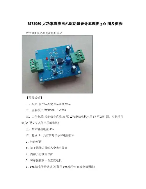
BTS7960大功率直流电机驱动器设计原理图pcb图及例程BTS7960大功率直流电机驱动【简要说明】一、尺寸:长76mmX宽65mmX高28mm二、主要芯片:BTS7960、lm2576三、工作电压:控制信号直流3V至12V;驱动电机电压6V至27V 四、可驱动直流(6V至27V之间电压的电机)五、最大输出电流43A六、特点:1、具有信号指示和电源指示2、转速可调3、抗干扰能力强输入全光电隔离4、内部具有续流保护5、可单独控制一台直流电机6、PWM脉宽平滑调速(可使用PWM信号对直流电机调速)7、可实现正反转8、此驱动器非常适合控制飞思卡尔智能车,驱动器压降小,电流大,驱动能力强适用场合:单片机学习、电子竞赛、产品开发、毕业设计。
1【标注图片】【应用事例】BTS7960直流电机驱动器控制表接线表:序号标号接线1 VCC 接控制信号的电源正极22 EN 控制信号使能端3 IN1 控制信号14 IN2 控制信号25 OUT1 接直流电机线6 OUT2 接直流电机线7 GND 控制电机的电源负极8 VSS 控制电机的电源正极控制方式表:EN IN1 IN2 实际输出驱动电流电机工作状态 L L L OUT1和OUT2都流出电流电机不转 L L H OUT1流出,OUT2流入电机正转 L H L OUT1流入,OUT2流出电机反转 H L L 无电流流出电机停止 H L H 无电流流出电机停止 H H L 无电流流出电机停止【测试程序】/******************************************************************* *汇诚科技实现功能:BTS7960大功率直流电机驱动_调试程序使用芯片:AT89S52 或者 STC89C52晶振:11.0592MHZ编译环境:Keil作者:zhangxinchun淘宝店:汇诚科技【声明】此程序仅用于学习与参考,引用请注明版权和作者信息~3******************************************************************** */#include<reg52.h>#define uchar unsigned char//宏定义无符号字符型 #define uint unsigned int //宏定义无符号整型sbit P2_0=P2^0;//启动sbit P2_1=P2^1;//停止sbit P2_2=P2^2;//正转sbit P2_3=P2^3;//反转sbit P1_0=P1^0;//使能sbit P1_1=P1^1;//IN1 sbit P1_2=P1^2;//IN2/******************************************************************* *延时函数******************************************************************** */void delay(uchar t)//延时程序{uchar m,n,s;for(m=t;m>0;m--)for(n=20;n>0;n--)for(s=248;s>0;s--); }/******************************************************************* *主函数******************************************************************** */main(){while(1){if(P2_0==0){delay(3);if(P2_0==0)//启动{P1_0=0;}}if(P2_1==0){delay(3);if(P2_1==0)//停止{P1_0=1;}}if(P2_2==0){delay(3);if(P2_2==0)//正转4{P1_1=1;P1_2=0;}}if(P2_3==0){delay(3);if(P2_3==0)//反转{P1_1=0;P1_2=1;}}}}/******************************************************************* *结束******************************************************************** */【应用原理图】【PCB尺寸图】5BTS7960智能功率芯片中文资料BTS7960是NovalithIC家族三个独立的芯片的一部分:一是p型通道的高电位场效应晶体管,二是一个n型通道的低电位场效应晶体管,结合一个驱动晶片,形成一个完全整合的高电流半桥。
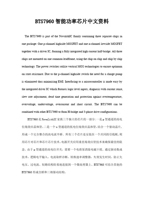
智能车竞赛中直流电机调速系统的设计与比较王名发,江智军,邹会权 时间:2009年12月04日字 体:关键词:直流电机调速系统MC33886VNH3SP30BTS7960BDT340IIRF3205摘 要:针对大学生智能车竞赛中直流电机的驱动设计了6种方案,经过实验比较分析了各种方案的优缺点,最后确立了一套驱动能力强、体积小、性能稳定的驱动方法,可广泛应用于40 V以下的大功率直流电机驱动的场合。
关键词:直流电机;调速系统; MC33886; VNH3SP30; BTS7960B; DT340I; IRF3205目前大电流直流电机多采用达林顿管或MOS管搭制H桥PWM脉宽调制,因此体积较大;另一方面,由于分立器件的特性不同,使得驱动器的特性具有一定的离散性;此外,由于功率管的开关电阻比较大,因此功耗也很大,需要功率的散热片,这无疑进一步加大了驱动器的体积。
随着技术的迅猛发展,基于大功率MOS管的H桥驱动芯片逐渐显现出其不可替代的优势。
但目前能提供较大电流输出的集成芯片不是很多。
例如飞思卡尔半导体公司推出的全桥驱动芯片MC33886和33887、意法半导体公司推出的全桥驱动芯片VNH3SP30、英飞凌公司推出的高电流PN半桥驱动芯片BTS7960。
ST微电子公司推出的TD340驱动器芯片是一种用于直流电机的控制器件,可用于驱动N沟道MOSFET管。
本文在第三、四届大学生智能车大赛中分别尝试了上面提到的5块电机驱动芯片设计的驱动电路,通过现场调试发现它们的优缺点,确定了驱动能力强、性能稳定的驱动方案,并得到了很好的应用。
1 直流电机驱动原理目前直流电机的驱动方式主要有2种形式:线性驱动方式和开关驱动方式。
其中线性驱动方式可以看成一个数控电压源。
该驱动方式的优点是驱动电机的力矩纹波很小,可应用于对电机转速要求非常高的场合;缺点是该方式通常比较复杂,成本较高,尤其是要提高驱动的功率时,相应的电路成本将提升很多[1]。

BTS7970-BTS7960及其他直流电机驱动模块在机械设备中,电机的作用非常重要,而它们的使用涉及到很多细节,其中就包括电机驱动模块。
直流电机驱动模块的作用就是将控制信号转换为电动机信号,从而使电动机正常工作。
本文将介绍其中的一些常见型号,包括BTS7970和BTS7960。
什么是BTS7970?BTS7970是一种直流电机驱动模块,由Infineon公司生产。
它的主要特点包括:•可以承受最大43A输出电流•能够在高达60V的电压下工作•具有低内部阻抗•内置过热保护和过电流保护功能这款模块通常被用于电动汽车、无人机和机器人等需要高功率的应用。
值得注意的是,BTS7970模块需要配合外部控制器使用,以便能够正确驱动电机。
什么是BTS7960?BTS7960也是一种直流电机驱动模块,同样由Infineon公司生产。
相比BTS7970,它的最大输出电流稍小,只有40A,并且在高压(30V至57V)应用下工作。
另外,BTS7960也具有高效的功能如短路保护、过热保护以及过电流保护,以确保设备的安全性。
如何选择正确的直流电机驱动模块?选择直流电机驱动模块时,需要考虑一系列因素。
确认电机参数电机的参数,如电流、电压、功率,都会影响模块的选择。
不同电机需要不同电流输出,因此需要为电机选择与其匹配的模块。
确认电机与控制器的接口除了电机的参数外,还需要考虑控制器与驱动器之间的接口是否兼容。
这将涉及到电机的控制方式,如PWM(脉冲宽度调制)、模拟信号控制或串行通信控制。
控制器与驱动模块之间的接口必须匹配,否则电机将无法正常工作。
确认被驱动的负载最后,需要确定被驱动的负载类型,如风扇、泵、飞行器或车辆。
这是因为不同的负载具有不同的动态特性,而电机驱动模块的选型也会受到这些因素的影响。
直流电机驱动模块的应用直流电机驱动模块广泛应用于自动化设备、电动车、轨道交通、船舶、机器人等方面。
以下是一些直流电机驱动模块的常见应用场景:电动车在电动车中,直流电机驱动模块做为中间设备,将电池组的直流电能转换为电机的转动动能。
BTS7960智能功率芯片中文资料The BTS7960 is part of the NovalithIC family containing three separate chips in one package: One p-channel highside MOSFET and one n-channel lowside MOSFET together with a driver IC, forming a fully integrated high current half-bridge. All three chips are mounted on one common leadframe, using the chip on chip and chip by chip technology. The power switches utilize vertical MOS technologies to ensure optimum on state resistance. Due to the p-channel highside switch the need for a charge pump is eliminated thus minimizing EMI. Interfacing to a microcontroller is made easy by the integrated driver IC which features logic level inputs, diagnosis with current sense, slew rate adjustment, dead time generation and protection against overtemperature, overvoltage, undervoltage, overcurrent and short circuit. The BTS7960 can be combined with other BTS7960 to form H-bridge and 3-phase drive configurations.BTS7960是NovalithIC家族三个独立的芯片的一部分:一是p型通道的高电位场效应晶体管,二是一个n型通道的低电位场效应晶体管,结合一个驱动晶片,形成一个完全整合的高电流半桥。
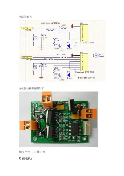
电路图如下:电机驱动板实物图如下如图所示:J1接电池;J5接电机;J6(黄色接头)提供5V电源;J6(白色接头)分别是1脚PWM口;2、3脚是控制方向和刹车单片机I/O口给01,是电机正转,10是电机反转,11是刹车。
注意:PWM是反逻辑,因为在单片机与电机驱动间加了反向驱动隔离,保护单片机。
所以占空比越小,方向后是越大,速度越快。
注意:PWM频率最大25KHZ,用在智能车上1KHZ就足够了。
MC9S12XS128测试程序如下I N H 3I N 2I S 6V S 7O U T4G N D 1S R 5J 3B T S 7960I N H 3I N 2I S 6V S7O U T4G N D1S R 5J 4B T S 7960R 31K R 4100R 71K R 8100R 101K R 61K 7.2V7.2VO U T 2O U T 1R 5 1K R 91KC 5100u F C 7100u F C 6104C 810412J 5M O T O RO U T 1O U T 212J 1P O W E RC 40.1u F C 20.1u F C 3100u F /16V C 1100u F /25VV i n 1G N D2+5V 3U 2L M 2940T -5.05VD 1LE D 3R 117.2V E N A B L EE N A B L EI N 1I N 2R T 2R T 1E N A B L E 1B 12B 23B 34B 45B 56B 67B 78B 8G N D 9C O M 108C 117C 126C 135C 144C 153C 162C 171C 18U 1U L N 2803A4132J 64P I NI N 1I N 2R 14K 7R 24K 75VR T 1R T 25V#include <hidef.h> /* common defines and macros */#include "derivative.h" /* derivative-specific definitions *//************************************************//*锁相环倍频*//************************************************/void pll_xs(void){SYNR=0x44;REFDV=0x81;//总线频率40Mwhile(!CRGFLG_LOCK);while(CLKSEL_PLLSEL!=1)CLKSEL_PLLSEL=1;}/***********************************************//*PWM初始化!*//************************************************/void PWM_int(void){PWMPOL|=0xaa;//PWM Polarity开始输出高电平,1、3、5、7 positive.PWMCLK|=0xaa;//Clock Select, Sn,B:7632.A:0145PWMPRCLK=0x22;//CLOCKA和CLOCKB是4分频是10MPWMCTL=0xf0;PWMSCLA=5;//1MPWMSCLB=5;//1MPWMCAE=0x00;PWMDTY01=900;PWMPER01=1000;PWME=0xaa; //PWM Enable,1、3、5、7 enable.}/************************************************/void main(void) {pll_xs();//倍频DDRB=0xff;PORTB|=0xff;PORTB&=0xfe;//PB0和PB1用来控制电机转向的EnableInterrupts;PWM_int();for(;;) {_FEED_COP(); /* feeds the dog */} /* loop forever *//* please make sure that you never leave main */}。

基于半导体制冷片的温度控制系统的设计摘要:设计一种用于红外传感器工作温度调节控制的模块,使红外传感器在低温下工作,以提高红外传感器的探测性能。
通过以mega16芯片为核心,以半导体制冷片为制冷元件,以PID算法为基础构建了一套半导体温度调节系统[1]。
实验结果表明,半导体制冷温度控制系统能够为红外探测器提供所需的工作温度。
关键词:温度半导体制冷片PID算法温度对红外传感器有比较大的影响,当外界环境温度发生变化时,红外传感器对所测量的物理量会有较大的变动,影响其测量值的准确性[2],产生较大的外界噪声干扰,所以当进行精确测量时,将红外传感器控制在一个恒定的温度下,可以大大提高探测精度,减少误差。
1 半导体制冷器的工作原理半导体制冷也称热电制冷,是一门介于制冷技术和半导体技术边缘的学科,半导体制冷是以温差电现象为基础制冷方法,利用帕尔贴效应的原理达到制冷目的。
帕尔帖效应:当电流I通过由两种不同材料组合成的闭合回路时,在材料的接头处一端会吸收热量Qp,另一端会放出热量Qp。
这种吸收或放出的热量叫做帕尔帖热,其吸热或放热由电流的方向决定,大小由公式决定。
π为帕尔帖系数,与温差电动势率有关,为组成回路两种材料的温差电动势率,T为相关接头的温度。
作为一种制冷源,半导体冷片可连续工作,不需要制冷剂,没有污染源和机械运动部件,不会产生回转效应,是一种固体元件,工作时没有噪音、震动、寿命长,安装容易。
半导体制冷片是电流换能型器件,通过控制输入电流,可实现高精度的温度控制。
热惯性小,制冷制热时间比较快,在热端散热良好冷端空载的情况下,可迅速达到最大温差。
2 温度控制系统的组成半导体温度控制系统结构框图如图1,由制冷片引起的温度变化经温度传感器传送给控制器,与设定的温度进行比较,所得的信号偏差通过PID进行调整处理,由控制器发出命令信号,通过驱动电路驱动半导体制冷片进行制热或者制冷,以达到红外传感器的工作温度环境。
3 硬件系统设计本控制系统主控单元采用的是ATMEL公司A VR系列的Atmega16单片机。
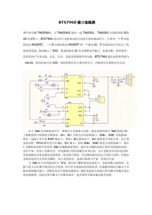
BTS7960接口连线图图中的引脚7960INH1、与7960INH2接在一起7960IN1、7960IN2分别连接到XS1 28的I/0口。
BTS7960是应用于电机驱动的大电流半桥高集成芯片,它带有一个P沟道的高边MOSFET、一个N沟道的低边MOSFET和一个驱动IC。
P沟道高边开关省去了电荷泵的需求, 因而减小了EMI。
集成的驱动IC具有逻辑电平输入、电流诊断、斜率调节、死区时间产生和过温、过压、欠压、过流及短路保护的功能。
BTS7960通态电阻典型值为16mΩ,驱动电流可达43A。
因此即使在北方寒冷的冬天,仍能保证车窗的安全启动。
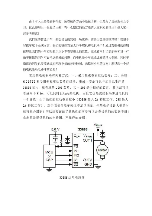
由于7960是单桥驱动芯片,要想让点击能够正反转,就必须使用两片7960构成全桥,上图就是两片构成的全桥驱动,IN1、IN2分别为方向控制端口,INH1、INH2为使能端,接在一起接上单片机PMW输出口,例如:IN1接高电平,IN2接低电平电机正传,反之则电机反转。
PWM脉冲也可由IN1、IN2输入,此时INH1、INH2就是方向控制端口。
接在5引脚的电容的作用是使7960的通断速度更快,接在各引脚的电阻主要作用是限流电阻,也可不加,但加上对跟安全,在电源端口的电容耐压必须注意,由于电机存在反向电动势,电容的耐压应是电源电压的两倍,更高则不需要,不仅增加成本还会占用更大体积,否则会导致电容发生击穿甚至爆炸,本人亲身经历,造成后果相当严重,望各位注意。
与7960差不多的驱动芯片7970,相比较7970驱动电流更大,其他参数大致相同。
在做飞思卡尔比赛中使用此芯片较多,在汽车车窗驱动也用的较多。
在做板布线时引脚4与引脚8都是输出端口,引脚8是芯片背面金属部分,输出电流很大如果只用引脚4的输出将会使布线烧毁,因此应将引脚4与引脚8接在一起并使用引脚8输出接至电机。
BTS7960中文资料[1]1BTS7960智能功率芯片中文资料The BTS7960 is part of the NovalithIC family containing threeseparate chips in one package: One p-channel highside MOSFET and one n-channel lowside MOSFET together with a driver IC, forming a fully integrated high current half-bridge. All three chips are mounted on one common leadframe, using the chip on chip and chip by chip technology. The power switches utilize vertical MOS technologies to ensure optimumon state resistance. Due to the p-channel highside switch the need for a charge pump is eliminated thus minimizing EMI. Interfacing to a microcontroller is made easy by the integrated driver IC which features logic level inputs, diagnosis with current sense, slew rate adjustment, dead time generation and protection against overtemperature, overvoltage, undervoltage, overcurrent and short circuit. The BTS7960 can be combined with other BTS7960 to form H-bridge and 3-phase drive configurations.BTS7960是NovalithIC家族三个独立的芯片的一部分:一是p型通道的高电位场效应晶体管,二是一个n型通道的低电位场效应晶体管,结合一个驱动晶片,形成一个完全整合的高电流半桥。
BTS7960High Current PN Half Bridge NovalithIC43A, 7mΩ + 9mΩTMHigh Current PN Half BridgeBTS7960Product Summary . . . . . . . . . . . . . . . . . . . . . . . . . . . . . . . . . . . . . . . . . . . . . . . . . . . .2 Basic Features . . . . . . . . . . . . . . . . . . . . . . . . . . . . . . . . . . . . . . . . . . . . . . . . . . . . . . .2 1Overview . . . . . . . . . . . . . . . . . . . . . . . . . . . . . . . . . . . . . . . . . . . . . . . . . . . . . . . . .3 1.1Block Diagram . . . . . . . . . . . . . . . . . . . . . . . . . . . . . . . . . . . . . . . . . . . . . . . . . . .3 1.2Terms . . . . . . . . . . . . . . . . . . . . . . . . . . . . . . . . . . . . . . . . . . . . . . . . . . . . . . . . .4 2Pin Configuration . . . . . . . . . . . . . . . . . . . . . . . . . . . . . . . . . . . . . . . . . . . . . . . . . .5 2.1Pin Assignment . . . . . . . . . . . . . . . . . . . . . . . . . . . . . . . . . . . . . . . . . . . . . . . . . .5 2.2Pin Definitions and Functions . . . . . . . . . . . . . . . . . . . . . . . . . . . . . . . . . . . . . . .5 3Maximum Ratings . . . . . . . . . . . . . . . . . . . . . . . . . . . . . . . . . . . . . . . . . . . . . . . . . .6 4Block Description and Characteristics. . . . . . . . . . . . . . . . . . . . . . . . . . . . . . . . .7 4.1Supply Characteristics . . . . . . . . . . . . . . . . . . . . . . . . . . . . . . . . . . . . . . . . . . . . .7 4.2Power Stages . . . . . . . . . . . . . . . . . . . . . . . . . . . . . . . . . . . . . . . . . . . . . . . . . . .84.2.1Power Stages - Static Characteristics . . . . . . . . . . . . . . . . . . . . . . . . . . . . 94.2.2Switching Times . . . . . . . . . . . . . . . . . . . . . . . . . . . . . . . . . . . . . . . . . . . 104.2.3Power Stages - Dynamic Characteristics . . . . . . . . . . . . . . . . . . . . . . . . 11 4.3Protection Functions . . . . . . . . . . . . . . . . . . . . . . . . . . . . . . . . . . . . . . . . . . . . .134.3.1Overvoltage Lock Out . . . . . . . . . . . . . . . . . . . . . . . . . . . . . . . . . . . . . . . 134.3.2Undervoltage Shut Down . . . . . . . . . . . . . . . . . . . . . . . . . . . . . . . . . . . . . 134.3.3Overtemperature Protection . . . . . . . . . . . . . . . . . . . . . . . . . . . . . . . . . . 134.3.4Current Limitation . . . . . . . . . . . . . . . . . . . . . . . . . . . . . . . . . . . . . . . . . . 134.3.5Short Circuit Protection . . . . . . . . . . . . . . . . . . . . . . . . . . . . . . . . . . . . . . 154.3.6Electrical Characteristics - Protection Functions . . . . . . . . . . . . . . . . . . . 16 4.4Control and Diagnostics . . . . . . . . . . . . . . . . . . . . . . . . . . . . . . . . . . . . . . . . . .174.4.1Input Circuit . . . . . . . . . . . . . . . . . . . . . . . . . . . . . . . . . . . . . . . . . . . . . . . 174.4.2Dead Time Generation . . . . . . . . . . . . . . . . . . . . . . . . . . . . . . . . . . . . . . 174.4.3Adjustable Slew Rate . . . . . . . . . . . . . . . . . . . . . . . . . . . . . . . . . . . . . . . 174.4.4Status Flag Diagnosis With Current Sense Capability . . . . . . . . . . . . . . 174.4.5Truth Table . . . . . . . . . . . . . . . . . . . . . . . . . . . . . . . . . . . . . . . . . . . . . . . 194.4.6Electrical Characteristics - Control and Diagnostics . . . . . . . . . . . . . . . . 20 5Thermal Characteristics . . . . . . . . . . . . . . . . . . . . . . . . . . . . . . . . . . . . . . . . . . . .21 6Application . . . . . . . . . . . . . . . . . . . . . . . . . . . . . . . . . . . . . . . . . . . . . . . . . . . . . . .22 6.1Application Example . . . . . . . . . . . . . . . . . . . . . . . . . . . . . . . . . . . . . . . . . . . . .22 6.2Layout Considerations . . . . . . . . . . . . . . . . . . . . . . . . . . . . . . . . . . . . . . . . . . . .22 7Package Outlines P-TO-263-7 . . . . . . . . . . . . . . . . . . . . . . . . . . . . . . . . . . . . . . .23 8Package Outlines P-TO-220-7 . . . . . . . . . . . . . . . . . . . . . . . . . . . . . . . . . . . . . . .24 9Revision History . . . . . . . . . . . . . . . . . . . . . . . . . . . . . . . . . . . . . . . . . . . . . . . . . .25Type Ordering Code Package BTS 7960B Q67060-S6160P-TO-263-7BTS 7960Pon requestP-TO-220-7High Current PN Half Bridge NovalithICBTS 7960B BTS 7960PProduct SummaryThe BTS 7960 is a fully integrated high current half bridge for motor drive applications. It is part of the NovalithIC TM family containing one p-channel highside MOSFET and one n-channel lowside MOSFET with an integrated driver IC in one package. Due to the p-channel highside switch the need for a charge pump is eliminated thus minimizing EMI. Interfacing to a microcontroller is made easy by the integrated driver IC which features logic level inputs, diagnosis with current sense, slew rate adjustment, dead time generation and protection against overtemperature, overvoltage, undervoltage,overcurrent and short circuit.The BTS 7960 provides a cost optimized solution for protected high current PWM motor drives with very low board space consumption.Basic Features•Path resistance of typ. 16m Ω@25°C •Low quiescent current of typ. 7µA @25°C•PWM capability of up to 25kHz combined with active freewheeling•Switched mode current limitation for reduced power dissipation in overcurrent •Current limitation level of 43A typ.•Status flag diagnosis with current sense capability •Overtemperature shut down with latch behaviour •Overvoltage lock out •Undervoltage shut down•Driver circuit with logic level inputs•Adjustable slew rates for optimized EMIBTS 7960B P-TO-263-7BTS 7960P P-TO-220-7TM1OverviewThe BTS7960 is part of the NovalithIC family containing three separate chips in one package: One p-channel highside MOSFET and one n-channel lowside MOSFET together with a driver IC, forming a fully integrated high current half-bridge. All three chips are mounted on one common leadframe, using the chip on chip and chip by chip technology. The power switches utilize vertical MOS technologies to ensure optimum on state resistance. Due to the p-channel highside switch the need for a charge pump is eliminated thus minimizing EMI. Interfacing to a microcontroller is made easy by the integrated driver IC which features logic level inputs, diagnosis with current sense, slew rate adjustment, dead time generation and protection against overtemperature, overvoltage, undervoltage, overcurrent and short circuit. The BTS7960 can be combined with other BTS7960 to form H-bridge and 3-phase drive configurations.1.1Block DiagramFigure1Block Diagram1.2TermsFollowing figure shows the terms used in this data sheet.Figure2TermsPin Configuration2Pin Configuration2.1Pin AssignmentFigure 3Pin Assignment BTS 7960B and BTS 7960P (top view)2.2Pin Definitions and FunctionsBold type: pin needs power wiringPin Symbol I/O Function 1GND -Ground2IN I InputDefines whether high- or lowside switch is activated 3INH I InhibitWhen set to low device goes in sleep mode 4,8OUT OPower output of the bridge5SRI Slew RateThe slew rate of the power switches can be adjusted by connecting a resistor between SR and GND 6IS O Current Sense and Diagnosis 7VS-SupplyMaximum Ratings3Maximum RatingsNote:Maximum ratings are absolute ratings; exceeding any one of these values maycause irreversible damage to the device. Exposure to maximum rating conditions for extended periods of time may affect device reliability-40 °C < T j < 150°C (unless otherwise specified)PosParameterSymbolLimits UnitTest Conditionminmax Electrical Maximum Ratings 3.0.1Supply voltageV VS-0.345V 3.0.2Logic Input Voltage V INV INH-0.3 5.3V 3.0.3HS/LS continuous drain currentI D(HS)I D(LS)-40401)1)Maximum reachable current may be smaller depending on current limitation levelA T C < 85°C switch active 3.0.4HS pulsed drain current I D(HS)-60601)A T C < 85°Ct pulse = 10ms3.0.5LS pulsed drain currentI D(LS)-60601)A 3.0.6Voltage at SR pin V SR-0.3 1.0V 3.0.7Voltage between VS and IS pinV VS -V IS-0.345V 3.0.8Voltage at IS pin V IS -2045V Thermal Maximum Ratings 3.0.9Junction temperatureT j -40150°C 3.0.10Storage temperature T stg -55150°C ESD Susceptibility3.0.11ESD susceptibility HBMIN, INH, SR, IS OUT, GND, VSV ESD-2-626kVaccording to EIA/JESD 22-A 114B4Block Description and Characteristics4.1Supply Characteristics– 40 °C < T j < 150 °C, 8 V < V S < 18 V, I L = 0A (unless otherwise specified)Pos.Parameter Symbol Limit Values Unit Test Conditionsmin.typ.max.General4.1.1Operating Voltage V S5.5–27.5V4.1.2Supply Current I VS(on)–23mA V INH = 5VV IN=0V or5VR SR=0ΩDC-modenormal operation(no fault condition) 4.1.3Quiescent Current I VS(off)–715µA V INH = 0VV IN=0V or5VT j <85°C––65µA V INH = 0VV IN=0V or5V4.2Power StagesThe power stages of the BTS7960 consist of a p-channel vertical DMOS transistor for the high side switch and a n-channel vertical DMOS transistor for the low side switch. All protection and diagnostic functions are located in a separate top chip. Both switches can be operated up to 25 kHz, allowing active freewheeling and thus minimizing power dissipation in the forward operation of the integrated diodes.The on state resistance R ON is dependent on the supply voltage V S as well as on the junction temperature T j . The typical on state resistance characteristics are shown in Figure 4.Figure4Typical On State Resistance vs. Supply Voltage4.2.1Power Stages - Static Characteristics– 40 °C < T j < 150 °C, 8 V < V S < 18 V (unless otherwise specified)Pos.Parameter Symbol Limit Values Unit Test Conditionsmin.typ.max.High Side Switch - Static Characteristics 4.2.1On state high sideresistanceR ON(HS)––710912.5m ΩI OUT = 9A V S = 13.5V T j = 25°C T j = 150°C 4.2.2Leakage current high sideI L(LKHS)––1µAV INH = 0V V OUT = 0V T j < 85 °C ––50µAV INH = 0V V OUT = 0 V T j = 150 °C 4.2.3Reverse diodeforward-voltage high side 1)1)Due to active freewheeling, diode is conducting only for a few µs, depending on R SRV DS(HS)–––0.90.80.61.51.10.8VI OUT =-9A T j = -40 °C T j = 25 °C T j = 150 °C Low Side Switch - Static Characteristics 4.2.4On state low side resistanceR ON(LS)––9141218m ΩI OUT =-9A V S = 13.5V T j = 25 °C T j = 150 °C 4.2.5Leakage current low sideI L(LKLS)––1µAV INH = 0V V OUT = V S T j < 85 °C ––15µAV INH = 0V V OUT = V S T j = 150 °C 4.2.6Reverse diodeforward-voltage low side 1)V SD(LS)–––0.90.80.61.51.10.8VI OUT = 9A T j = -40 °C T j = 25 °C T j = 150 °C4.2.2Switching TimesFigure 5Definition of switching times high side (R load to GND)Figure 6Definition of switching times low side (R load to VS)Due to the timing differences for the rising and the falling edge there will be a slight difference between the length of the input pulse and the length of the output pulse. It can be calculated using the following formulas:•∆t HS = (t dr(HS) + 0.5 t r(HS)) - (t df(HS) + 0.5 t f(HS))•∆t LS = (t df(LS) + 0.5 t f(LS)) - (t dr(LS) + 0.5 t r(LS)).4.2.3Power Stages - Dynamic Characteristics-40 °C < T j < 150 °C, V S = 13.5 V, R load = 2Ω (unless otherwise specified)Pos.Parameter Symbol Limit Values Unit Test Conditionsmin.typ.max.HIgh Side Switch Dynamic Characteristics4.2.7Rise-time of HS t r(HS)0.5–2.81271.5–11µsR SR = 0ΩR SR = 5.1kΩR SR = 51kΩ4.2.8Slew rate HS on∆V OUT/t r( HS)–––1161.6–––V/µsR SR = 0ΩR SR = 5.1kΩR SR = 51kΩ4.2.9Switch on delay timeHS t dr(HS)1.7–5.63.14.4144.5–22.4µsR SR = 0ΩR SR = 5.1kΩR SR = 51kΩ4.2.10Fall-time of HS t f(HS)0.5–2.81271.5–11µsR SR = 0ΩR SR = 5.1kΩR SR = 51kΩ4.2.11Slew rate HS off -∆V OUT/t f(HS)–––1161.6–––V/µsR SR = 0ΩR SR = 5.1kΩR SR = 51kΩ4.2.12Switch off delay timeHS t df(HS)1.2–42.43.4103.6–16µsR SR = 0ΩR SR = 5.1kΩR SR = 51kΩLow Side Switch Dynamic Characteristics4.2.13Rise-time of LS t r(LS)0.5–2.81271.5–11µsR SR = 0ΩR SR = 5.1kΩR SR = 51kΩ4.2.14Slew rate LS switch off ∆V OUT/t r(LS)–––1161.6–––V/µsR SR = 0ΩR SR = 5.1kΩR SR = 51kΩ4.2.15Switch off delay timeLS t dr(LS)0.7–2.81.32.271.9–11.2µsR SR = 0ΩR SR = 5.1kΩR SR = 51kΩ4.2.16Fall-time of LS t f(LS)0.5–2.81271.5–11µsR SR = 0ΩR SR = 5.1kΩR SR = 51kΩ4.2.17Slew rate LS switch on -∆V OUT/t f(LS)–––1161.6–––V/µsR SR = 0ΩR SR = 5.1kΩR SR = 51kΩ4.2.18Switch on delay timeLS t df(LS)2.2–6.445.6165.8–25.4µsR SR = 0ΩR SR = 5.1kΩR SR = 51kΩ-40 °C < T j < 150 °C, V S = 13.5 V, R load = 2Ω (unless otherwise specified)Pos.Parameter Symbol Limit Values Unit Test Conditionsmin.typ.max.4.3Protection FunctionsThe device provides integrated protection functions. These are designed to prevent IC destruction under fault conditions described in the data sheet. Fault conditions are considered as “outside” normal operating range. Protection functions are not to be used for continuous or repetitive operation, with the exception of the current limitation (Chapter4.3.4). In a fault condition the BTS7960 will apply the highest slew rate possible independent of the connected slew rate resistor. Overvoltage, overtemperature and overcurrent are indicated by a fault current I IS(LIM) at the IS pin as described in the paragraph “Status Flag Diagnosis With Current Sense Capability” on Page17 and Figure10.In the following the protection functions are listed in order of their priority. Overvoltage lock out overrides all other error modes.4.3.1Overvoltage Lock OutTo assure a high immunity against overvoltages (e.g. load dump conditions) the device shuts the lowside MOSFET off and turns the highside MOSFET on, if the supply voltage is exceeding the over voltage protection level V OV(OFF). The IC operates in normal mode again with a hysteresis V OV(HY) if the supply voltage decreases below the switch-onvoltage V OV(ON). In H-bridge configuration, this behavior of the BTS7960 will lead to freewheeling in highside during over voltage.4.3.2Undervoltage Shut DownTo avoid uncontrolled motion of the driven motor at low voltages the device shuts off (output is tri-state), if the supply voltage drops below the switch-off voltage V UV(OFF). The IC becomes active again with a hysteresis V UV(HY) if the supply voltage rises above theswitch-on voltage V UV(ON).4.3.3Overtemperature ProtectionThe BTS7960 is protected against overtemperature by an integrated temperature sensor. Overtemperature leads to a shut down of both output stages. This state is latched until the device is reset by a low signal with a minimum length of t reset at the INH pin, provided that its temperature has decreased at least the thermal hysteresis ∆T in themeantime.Repetitive use of the overtemperature protection might reduce lifetime.4.3.4Current LimitationThe current in the bridge is measured in both switches. As soon as the current in forward direction in one switch (high side or low side) is reaching the limit I CLx, this switch is deactivated and the other switch is activated for t CLS . During that time all changes at theIN pin are ignored. However, the INH pin can still be used to switch both MOSFETs off.After t CLS the switches return to their initial setting. The error signal at the IS pin is reset after 2 * t CLS . Unintentional triggering of the current limitation by short current spikes (e.g. inflicted by EMI coming from the motor) is suppressed by internal filter circuitry. Due to thresholds and reaction delay times of the filter circuitry the effective current limitation level I CLx depends on the slew rate of the load current d I /d t as shown in Figure 8Figure 7Timing Diagram Current LimitationFigure 8Current Limitation Level vs. Current Slew Rate dI/dtFigure9Typical Current Limitation Detection Levels vs. Supply VoltageIn combination with a typical inductive load, such as a motor, this results in a switched mode current limitation. That way of limiting the current has the advantage that the power dissipation in the BTS7960 is much smaller than by driving the MOSFETs in linear mode. Therefore it is possible to use the current limitation for a short time without exceeding the maximum allowed junction temperature (e.g. for limiting the inrush current during motor start up). However, the regular use of the current limitation is allowed as long as the specified maximum junction temperature is not exceeded. Exceeding this temperature can reduce the lifetime of the device.4.3.5Short Circuit ProtectionThe device is short circuit protected against•output short circuit to ground•output short circuit to supply voltage•short circuit of loadThe short circuit protection is realized by the previously described current limitation in combination with the over-temperature shut down of the device4.3.6Electrical Characteristics - Protection Functions– 40 °C < T j < 150 °C; 8 V < V S < 18 V (unless otherwise specified)Pos.Parameter Symbol Limit Values Unit Test Conditionsmin.typ.max.Under Voltage Shut Down4.3.1Switch-ON voltage V UV(ON)––5.5V V S increasing 4.3.2Switch-OFF voltage V UV(OFF) 4.0– 5.4V V S decreasing 4.3.3ON/OFF hysteresis V UV(HY)–0.2–V–Over Voltage Lock Out4.3.4Switch-ON voltage V OV(ON)27.5––V V S decreasing 4.3.5Switch-OFF voltage V OV(OFF)27.6–30V V S increasing 4.3.6ON/OFF hysteresis V OV(HY)–0.2–V–Current Limitation4.3.7Current limitationdetection level highside I CLH0474443626059848079A V S=13.5VT j = -40 °CT j = 25 °CT j = 150 °C4.3.8Current limitationdetection level lowside I CLL0363433474342646161A V S=13.5VT j = -40 °CT j = 25 °CT j = 150 °CCurrent Limitation Timing4.3.9Shut off time for HSand LSt CLS70115210µs V S=13.5V Thermal Shut Down4.3.10Thermal shut downjunction temperatureT jSD152175200°C–4.3.11Thermal switch onjunction temperatureT jSO150–190°C–4.3.12Thermal hysteresis∆T–7–K–4.3.13Reset pulse at INH pin(INH low)t reset3––µs–4.4Control and Diagnostics4.4.1Input CircuitThe control inputs IN and INH consist of TTL/CMOS compatible schmitt triggers with hysteresis which control the integrated gate drivers for the MOSFETs. Setting the INH pin to high enables the device. In this condition one of the two power switches is switched on depending on the status of the IN pin. To deactivate both switches, the INH pin has to be set to low. No external driver is needed. The BTS7960 can be interfaced directly to a microcontroller.4.4.2Dead Time GenerationIn bridge applications it has to be assured that the highside and lowside MOSFET are not conducting at the same time, connecting directly the battery voltage to GND. This is assured by a circuit in the driver IC, generating a so called dead time between switching off one MOSFET and switching on the other. The dead time generated in the driver IC is automatically adjusted to the selected slew rate.4.4.3Adjustable Slew RateIn order to optimize electromagnetic emission, the switching speed of the MOSFETs is adjustable by an external resistor. The slew rate pin SR allows the user to optimize the balance between emission and power dissipation within his own application by connecting an external resistor R SR to GND.4.4.4Status Flag Diagnosis With Current Sense CapabilityThe status pin IS is used as a combined current sense and error flag output. In normal operation (current sense mode), a current source is connected to the status pin, which delivers a current proportional to the forward load current flowing through the active high side switch. If the high side switch is inactive or the current is flowing in the reverse direction no current will be driven except for a marginal leakage current I IS(LK). The external resistor R IS determines the voltage per output current. E.g. with the nominal value of 8500 for the current sense ratio k ILIS = I L / I IS, a resistor value of R IS = 1kΩ leads to V IS = (I L / 8.5 A)V. In case of a fault condition the status output is connected to a current source which is independent of the load current and provides I IS(lim). The maximum voltage at the IS pin is determined by the choice of the external resistor and the supply voltage. In case of current limitation the I IS(lim) is activated for 2 * t CLS.Figure10Sense current and fault current4.4.5Truth TableDevice State Inputs Outputs ModeINH IN HSS LSS ISNormal operation0X OFF OFF0Stand-by mode10OFF ON0LSS active11ON OFF CS HSS activeOver-voltage (OV)X X ON OFF1Shut-down of LSS,HSS activated,error detected Under-voltage (UV)X X OFF OFF0UV lockoutOvertemperature or short circuit of HSS or LSS 0X OFF OFF0Stand-by mode, resetof latch1X OFF OFF1Shut-down with latch,error detectedCurrent limitation mode11OFF ON1Switched mode, errordetected10ON OFF1Switched mode, errordetectedInputs:Switches Status Flag IS:0 = Logic LOW OFF = switched off CS = Current sense mode1 = Logic HIGH ON = switched on 1 = Logic HIGH (error)X = 0 or 1Block Description and Characteristics4.4.6Electrical Characteristics - Control and Diagnostics– 40 °C < T j < 150 °C, 8 V < V S < 18 V (unless otherwise specified)Pos.Parameter Symbol Limit Values Unit Test Conditionsmin.typ.max.Control Inputs (IN and INH)4.4.1High level voltageINH, IN V INH(H)V IN(H)– 1.751.62.152V–4.4.2Low level voltageINH, IN V INH(L)V IN(L)1.1 1.4–V–4.4.3Input voltagehysteresis V INHHYV INHY––350200––mV–4.4.4Input current I INH(H)I IN(H)–30150µA V IN = V INH= 5.3 V4.4.5Input current I INH(L)I IN(L)–25125µA V IN = V INH=0.4 V Current Sense4.4.6Current sense ratioin static on-conditionk ILIS = I L / I IS k ILIS6538.58.58.5111214103R IS = 1 kΩI L = 30AI L = 15AI L = 5A4.4.7Maximum analogsense current, sensecurrent in faultcondition I IS(lim)4 4.57mA V S = 13.5 VR IS = 1kΩ4.4.8Isense leakage current I ISL––1µA V IN= 0V orV INH= 0V4.4.9Isense leakage current,active high side switch I ISH–1200µA V IN = V INH= 5VI L= 0AThermal Characteristics 5Thermal CharacteristicsPos Parameter Symbol Limits Unit Test Conditionmin max5.0.1Thermal ResistanceJunction-Case, Low Side SwitchR thjc(LS) = ∆T j(LS)/ P v(LS)R thjc(LS)– 1.8K/W5.0.2Thermal ResistanceJunction-Case, High Side SwitchR thjc(HS) = ∆T j(HS)/ P v(HS)R thjc(HS)–0.9K/W5.0.3Thermal ResistanceJunction-Case, both SwitchesR thjc= max[∆T j(HS), ∆T j(LS)] /(P v(HS) + P v(LS))R thjc– 1.0K/W5.0.4Thermal ResistanceJunction-Ambient R thja–35K/W6cm2 coolingareaApplication 6ApplicationFigure11Application Example: H-Bridge with two BTS7960B6.2Layout ConsiderationsDue to the fast switching times for high currents, special care has to be taken to the PCB layout. Stray inductances have to be minimized in the power bridge design as it is necessary in all switched high power bridges. The BTS7960 has no separate pin for power ground and logic ground. Therefore it is recommended to assure that the offset between the ground connection of the slew rate resistor, the current sense resistor and ground pin of the device (GND / pin1) is minimized. If the BTS7960 is used in a H-bridge or B6 bridge design, the voltage offset between the GND pins of the different devices should be small as well.A ceramic capacitor from VS to GND close to each device is recommended to provide current for the switching phase via a low inductance path and therefore reducing noise and ground bounce. A reasonable value for this capacitor would be about 470 nF.The digital inputs need to be protected from excess currents (e.g. caused by induced voltage spikes) by series resistors in the range of 10 kΩ.7Package Outlines P-TO-263-7Y ou can find all of our packages, sorts of packing and others in ourInfineon Internet Page “Products”: /products.Dimensions in mm SMD = Surface Mounted Device8Package Outlines P-TO-220-7Y ou can find all of our packages, sorts of packing and others in ourInfineon Internet Page “Products”: /products.Dimensions in mmRevision History 9Revision HistoryRevision Date Changes / Commentsn.a.2004-03-18Target Data Sheet0.92004-10-10Target Data Sheet converted to new layout1.02004-11-30Preliminary Data Sheet1.12004-12-07“Preliminary” removed; No other changesEdition 2004-12-07Published by Infineon Technologies AG,St.-Martin-Strasse 53,D-81541 München, Germany© Infineon Technologies AG 2004-12-07.All Rights Reserved.Attention please!The information herein is given to describe certain components and shall not be considered as warranted characteristics.Terms of delivery and rights to technical change reserved.We hereby disclaim any and all warranties, including but not limited to warranties of non-infringement, regarding circuits, descriptions and charts stated herein.Infineon Technologies is an approved CECC manufacturer.InformationFor further information on technology, delivery terms and conditions and prices please contact your nearest Infineon Technologies Office in Germany or our Infineon Technologies Representatives worldwide.WarningsDue to technical requirements components may contain dangerous substances. For information on the types in question please contact your nearest Infineon Technologies Office.Infineon Technologies Components may only be used in life-support devices or systems with the express written approval of Infineon Technologies, if a failure of such components can reasonably be expected to cause the failure of that life-support device or system, or to affect the safety or effectiveness of that device or system. Life support devices or systems are intended to be implanted in the human body, or to support and/or maintain and sustain and/or protect human life. If they fail, it is reasonable to assume that the health of the user or other persons may be endangered.。