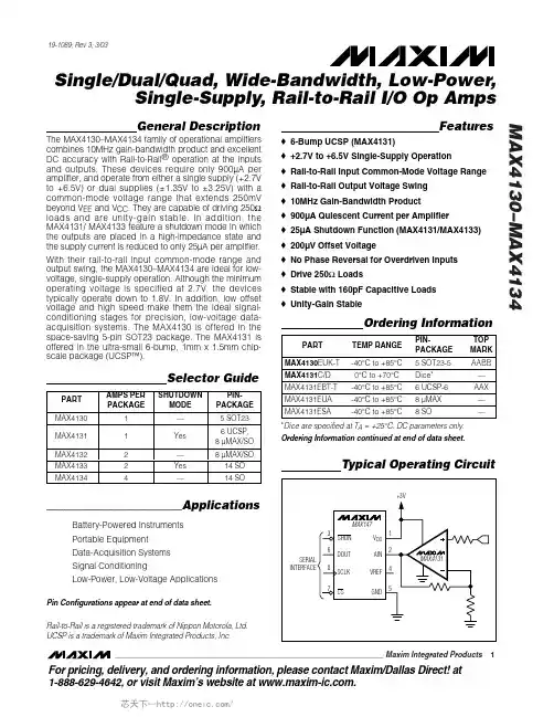
MAX4130–MAX4134________________________________________________________________Maxim Integrated Products1For pricing, delivery, and ordering information,please contact Maxim/Dallas Direct!at 1-888-629-4642, or visit Maxim’s website at .General DescriptionThe MAX4130–MAX4134 family of operational amplifiers combines 10MHz gain-bandwidth product and excellent DC accuracy with Rail-to-Rail ®operation at the inputs and outputs. These devices require only 900µA per amplifier, and operate from either a single supply (+2.7V to +6.5V) or dual supplies (±1.35V to ±3.25V) with a common-mode voltage range that extends 250mV beyond V EE and V CC . They are capable of driving 250Ωloads and are unity-gain stable. In addition, the MAX4131/ MAX4133 feature a shutdown mode in which the outputs are placed in a high-impedance state and the supply current is reduced to only 25µA per amplifier.With their rail-to-rail input common-mode range and output swing, the MAX4130–MAX4134 are ideal for low-voltage, single-supply operation. Although the minimum operating voltage is specified at 2.7V, the devices typically operate down to 1.8V. In addition, low offset voltage and high speed make them the ideal signal-conditioning stages for precision, low-voltage data-acquisition systems. The MAX4130 is offered in the space-saving 5-pin SOT23 package. The MAX4131 is offered in the ultra-small 6-bump, 1mm x 1.5mm chip-scale package (UCSP™).________________________ApplicationsBattery-Powered Instruments Portable Equipment Data-Acquisition Systems Signal ConditioningLow-Power, Low-Voltage ApplicationsFeatureso 6-Bump UCSP (MAX4131)o +2.7V to +6.5V Single-Supply Operationo Rail-to-Rail Input Common-Mode Voltage Rangeo Rail-to-Rail Output Voltage Swing o 10MHz Gain-Bandwidth Product o 900µA Quiescent Current per Amplifier o 25µA Shutdown Function (MAX4131/MAX4133)o 200µV Offset Voltageo No Phase Reversal for Overdriven Inputs o Drive 250ΩLoadso Stable with 160pF Capacitive Loads o Unity-Gain StableSingle/Dual/Quad, Wide-Bandwidth, Low-Power,Single-Supply, Rail-to-Rail I/O Op Amps19-1089; Rev 3; 3/03*Dice are specified at T A = +25°C. DC parameters only.Ordering Information continued at end of data sheet.Pin Configurations appear at end of data sheet.Rail-to-Rail is a registered trademark of Nippon Motorola, Ltd.UCSP is a trademark of Maxim Integrated Products, Inc.M A X 4130–M A X 4134Single/Dual/Quad, Wide-Bandwidth, Low-Power,Single-Supply Rail-to-Rail I/O Op Amps 2_______________________________________________________________________________________ABSOLUTE MAXIMUM RATINGSDC ELECTRICAL CHARACTERISTICS(V CC = +2.7V to +6.5V, V EE = 0V, V CM = 0V, V OUT = V CC /2, R L tied to V CC /2, SHDN ≥2V (or open), T A = +25°C , unless otherwise noted.)Stresses beyond those listed under “Absolute Maximum Ratings” may cause permanent damage to the device. These are stress ratings only, and functional operation of the device at these or any other conditions beyond those indicated in the operational sections of the specifications is not implied. Exposure to absolute maximum rating conditions for extended periods may affect device reliability.Supply Voltage (V CC - V EE )...................................................7.5V IN+, IN-, SHDN Voltage...................(V CC + 0.3V) to (V EE - 0.3V)Output Short-Circuit Duration (Note 1).......................Continuous(short to either supply)Continuous Power Dissipation (T A = +70°C)5-Pin SOT23 (derate 7.1mW/°C above +70°C)............571mW 6-Bump UCSP (derate 2.9mW/°C above +70°C).........308mW 8-Pin SO (derate 5.88mW/°C above +70°C)................471mW8-Pin µMAX (derate 4.10mW/°C above +70°C)...........330mW 14-Pin SO (derate 8.00mW/°C above +70°C)..............640mW Operating Temperature RangeMAX413_E__...................................................-40°C to +85°C Maximum Junction Temperature.....................................+150°C Storage Temperature Range.............................-65°C to +160°C Lead Temperature (soldering, 10s).................................+300°C Bump Reflow Temperature .........................................+235°CNote 1:Provided that the maximum package power-dissipation rating is not exceeded.MAX4130–MAX4134Single/Dual/Quad, Wide-Bandwidth, Low-Power,Single-Supply Rail-to-Rail I/O Op AmpsDC ELECTRICAL CHARACTERISTICS (continued)(V CC = +2.7V to +6.5V, V EE = 0V, V CM = 0V, V OUT = V CC /2, R L tied to V CC /2, SHDN ≥2V (or open), T A = +25°C , unless otherwise noted.)DC ELECTRICAL CHARACTERISTICS(V CC = +2.7V to +6.5V, V EE = 0V, V CM = 0V, V OUT = V CC /2, R L tied to V CC /2, SHDN ≥2V (or open), T A = -40°C to +85°C , unlessM A X 4130–M A X 4134Single/Dual/Quad, Wide-Bandwidth, Low-Power,Single-Supply Rail-to-Rail I/O Op Amps 4_______________________________________________________________________________________DC ELECTRICAL CHARACTERISTICS(V CC = +2.7V to +6.5V, V EE = 0V, V CM = 0V, V OUT = V CC /2, R L tied to V CC /2, SHDN ≥2V (or open), T A = -40°C to +85°C , unlessMAX4130–MAX4134Single/Dual/Quad, Wide-Bandwidth, Low-Power,Single-Supply Rail-to-Rail I/O Op Amps_______________________________________________________________________________________5DC ELECTRICAL CHARACTERISTICS (continued)(V CC = +2.7V to +6.5V, V EE = 0V, V CM = 0V, V OUT = V CC /2, R L tied to V CC /2, SHDN ≥2V (or open), T A = -40°C to +85°C , unless otherwise noted.) (Note 2)AC ELECTRICAL CHARACTERISTICSM A X 4130–M A X 4134Single/Dual/Quad, Wide-Bandwidth, Low-Power,Single-Supply, Rail-to-Rail I/O Op Amps 6_______________________________________________________________________________________60-401001k 10k 1M 10M100k 100M GAIN AND PHASE vs. FREQUENCY-20FREQUENCY (Hz)G A I N (d B )02040P H A S E (D E G R E E S )180144720-72-144-180-108-363610860-401001k 10k 1M 10M100k 100MGAIN AND PHASEvs. FREQUENCY (WITH C)-20FREQUENCY (Hz)G A I N (d B )2040P H A S E (D E G R E E S )180144720-72-144-180-108-36361080-100101001k100k1M10M10k 100MPOWER-SUPPLY REJECTIONvs. FREQUENCY-80FREQUENCY (Hz)P S R (d B )-60-40-2001051520253530454050-40-25-105203550658095SHUTDOWN SUPPLY CURRENTvs. TEMPERATURETEMPERATURE (°C)S U P P L Y C U R R E N T (µA )1000.100.011001k100k1M10M10k100MOUTPUT IMPEDANCE vs. FREQUENCYFREQUENCY (Hz)O U T P U T I M P E D A N C E (Ω)1101150800850900950105010001100-40-25-105203550658095SUPPLY CURRENT PER AMPLIFIERvs. TEMPERATURETEMPERATURE (°C)S U P P L Y C U R R E N T (µA )-10-505101520-40-25-105203550658095OUTPUT LEAKAGE CURRENTvs. TEMPERATURETEMPERATURE (°C)L E A K A G E C U R R E N T (µA )Typical Operating Characteristics(V CC = +5V, V EE = 0V, VCM = V CC / 2, T A = +25°C, unless otherwise noted.)-600123456INPUT BIAS CURRENT vs. COMMON-MODE VOLTAGECOMMON-MODE VOLTAGE (V)I N P U T B I A S C U R R E N T (n A )-50-40-30-20-10010203040-60-40-40-25-105203550658095INPUT BIAS CURRENTvs. TEMPERATURETEMPERATURE (°C)I N P U T B I A S C U R R E N T (n A )-200204060MAX4130–MAX4134Single/Dual/Quad, Wide-Bandwidth, Low-Power,Single-Supply, Rail-to-Rail I/O Op Amps_______________________________________________________________________________________712070750600110115OUTPUT VOLTAGE: EITHER SUPPLY (mV)G A I N (d B )30095859080100200500105100400LARGE-SIGNAL GAIN vs. OUTPUT VOLTAGE130-40-25-105203550658095LARGE-SIGNAL GAIN vs. TEMPERATURE90120TEMPERATURE (°C)G A I N (d B )11010085951251151051.21.31.51.41.61.71.81.9-40-25-105203550658095MINIMUM OPERATING VOLTAGEvs. TEMPERATUREM A X 4130/34-21TEMPERATURE (°C)M I N I M U M O P E R A T I N G V O L T A G E (V )Typical Operating Characteristics (continued)(V CC = +5V, V EE = 0V, V CM = V CC / 2, T A = +25°C, unless otherwise noted.)12080859095100105110115-40-25-105203550658095COMMON-MODE REJECTIONvs. TEMPERATURETEMPERATURE (°C)C O M M O N -M ODE R E J E C T I O N (d B )130700600120OUTPUT VOLTAGE: EITHER SUPPLY (mV)G A I N (dB )3001009080100200500110400LARGE-SIGNAL GAIN vs. OUTPUT VOLTAGE12060600110OUTPUT VOLTAGE: EITHER SUPPLY (mV)G A I N (d B )300908070100200500100400LARGE-SIGNAL GAIN vs. OUTPUT VOLTAGE12080-40-25-105203550658095LARGE-SIGNAL GAIN vs. TEMPERATURE90TEMPERATURE (°C)G A I N (d B )105859511511010012070750600110115OUTPUT VOLTAGE: EITHER SUPPLY (mV)G A I N (d B )30095859080100200500105100400LARGE-SIGNAL GAIN vs. OUTPUT VOLTAGE-3.00-2.25-0.75-1.5001.500.752.253.00-40-25-105203550658095INPUT OFFSET VOLTAGE vs. TEMPERATURETEMPERATURE (°C)V O L T A G E (m V )M A X 4130–M A X 4134Single/Dual/Quad, Wide-Bandwidth, Low-Power,Single-Supply, Rail-to-Rail I/O Op Amps 8_______________________________________________________________________________________1408010k 1k 100k 10M 1M CHANNEL SEPARATION vs. FREQUENCYFREQUENCY (Hz)C H A N N E L S E P A R A T I O N (d B )1009013011012010100k10kFREQUENCY (Hz)1001k 0.03000.0050.0100.0150.0200.025 TOTAL HARMONIC DISTORTION AND NOISE vs. FREQUENCYT H D A N D N O I S E (%)0.10.0014.04.44.25.04.84.6TOTAL HARMONIC DISTORTION AND NOISE vs. PEAK-TO-PEAK SIGNAL AMPLITUDEPEAK-TO-PEAK SIGNAL AMPLITUDE (V)T H D + N O I S E (%)0.01INTIME (200ns/div)V O L T A G E (50m V /d i v )OUTMAX4131SMALL-SIGNAL TRANSIENT RESPONSE (NONINVERTING)IN TIME (200ns/div)V O L T A G E (50m V /d i v )OUT MAX4131SMALL-SIGNAL TRANSIENT RESPONSE (INVERTING)A V = -1IN TIME (2µs/div)V O L T A G E (2V/d i v )OUT MAX4131LARGE-SIGNAL TRANSIENT RESPONSE (NONINVERTING)A V = +1INTIME (2µs/div)V O L T A G E (2V /d i v )OUTMAX4131LARGE-SIGNAL TRANSIENT RESPONSE (INVERTING)Typical Operating Characteristics (continued)(V CC = +5V, V EE = 0V, V CM = V CC / 2, T A = +25°C, unless otherwise noted.)1600-40-25-105203550658095MINIMUM OUTPUT VOLTAGEvs. TEMPERATURE20140120TEMPERATURE (°C)V O U T - V E E (m V )100806040050100150200250300-40-25-105203550658095MAXIMUM OUTPUT VOLTAGEvs. TEMPERATURETEMPERATURE (°C)V C C - V O U T (m V )MAX4130–MAX4134Single/Dual/Quad, Wide-Bandwidth, Low-Power,Single-Supply, Rail-to-Rail I/O Op Amps_______________________________________________________________________________________9Figure 1a. Reducing Offset Error Due to Bias Current (Noninverting)Figure 1b. Reducing Offset Error Due to Bias Current (Inverting)M A X 4130–M A X 4134Single/Dual/Quad, Wide-Bandwidth, Low-Power,Single-Supply, Rail-to-Rail I/O Op Amps 10______________________________________________________________________________________Applications InformationRail-to-Rail Input StageDevices in the MAX4130–MAX4134 family of high-speed amplifiers have rail-to-rail input and output stages designed for low-voltage, single-supply opera-tion. The input stage consists of separate NPN and PNP differential stages that combine to provide an input common-mode range that extends 0.2V beyond the supply rails. The PNP stage is active for input volt-ages close to the negative rail, and the NPN stage is active for input voltages near the positive rail. The input offset voltage is typically below 200µV. The switchover transition region, which occurs near V CC / 2, has been extended to minimize the slight degradation in com-mon-mode rejection ratio caused by the mismatch of the input pairs. Their low offset voltage, high band-width, and rail-to-rail common-mode range make these op amps excellent choices for precision, low-voltage data-acquisition systems.Since the input stage switches between the NPN and PNP pairs, the input bias current changes polarity as the input voltage passes through the transition region.Reduce the offset error caused by input bias currents flowing through external source impedances by match-ing the effective impedance seen by each input (Figures 1a, 1b). High source impedances, together with input capacitance, can create a parasitic pole that produces an underdamped signal response. Reducing the input impedance or placing a small (2pF to 10pF)capacitor across the feedback resistor improves response.The MAX4130–MAX4134s ’ inputs are protected from large differential input voltages by 1k Ωseries resistors and back-to-back triple diodes across the inputs (Figure 2). For differential input voltages less than 1.8V,input resistance is typically 500k Ω. For differential input voltages greater than 1.8V, input resistance is approxi-mately 2k Ω. The input bias current is given by the fol-lowing equation:Figure 2. Input Protection CircuitMAX4130–MAX4134Single/Dual/Quad, Wide-Bandwidth, Low-Power,Single-Supply, Rail-to-Rail I/O Op Amps______________________________________________________________________________________11Rail-to-Rail Output StageThe minimum output voltage is within millivolts of ground for single-supply operation where the load is referenced to ground (V EE ). Figure 3 shows the input voltage range and output voltage swing of a MAX4131connected as a voltage follower. With a +3V supply and the load tied to ground, the output swings from 0.00V to 2.90V. The maximum output voltage swing depends on the load, but will be within 150mV of a +3V supply, even with the maximum load (500Ωto ground).Driving a capacitive load can cause instability in most high-speed op amps, especially those with low quies-cent current. The MAX4130–MAX4134 have a high tol-erance for capacitive loads. They are stable with capacitive loads up to 160pF. Figure 4 gives the stable operating region for capacitive loads. Figures 5 and 6show the response with capacitive loads and the results of adding an isolation resistor in series with the output (Figure 7). The resistor improves the circuit ’s phase margin by isolating the load capacitor from the op amp ’s output.INTIME (1µs/div)V O L T A G E (1V /d i v )OUTV CC = 3V, R L = 10k Ω to V EEFigure 3. Rail-to-Rail Input/Output Voltage RangeFigure 4. Capacitive-Load StabilityINTIME (200ns/div)V O L T A G E (50m V /d i v )OUTV CC = 5V R L = 10k Ω C L = 130pFFigure 5. MAX4131 Small-Signal Transient Response with Capacitive Load Figure 6. MAX4131 Transient Response to Capacitive Load with Isolation ResistorINTIME (500ns/div)V O L T A G E (50m V /d i v )OUTV CC = 5V C L = 1000pF R S = 39ΩM A X 4130–M A X 4134Single/Dual/Quad, Wide-Bandwidth, Low-Power,Single-Supply, Rail-to-Rail I/O Op Amps 12______________________________________________________________________________________Power-Up and Shutdown ModeThe MAX4130–MAX4134 amplifiers typically settle with-in 1µs after power-up. Figures 9 and 10 show the out-put voltage and supply current on power-up, using the test circuit of Figure 8.The MAX4131 and MAX4133 have a shutdown option.When the shutdown pin (SHDN ) is pulled low, the sup-ply current drops below 25µA per amplifier and theamplifiers are disabled with the outputs in a high-impedance state. Pulling SHDN high or leaving it float-ing enables the amplifier. In the dual-amplifier MAX4133, the shutdown functions operate indepen-dently. Figures 11 and 12 show the output voltage and supply current responses of the MAX4131 to a shut-down pulse, using the test circuit of Figure 8.Figure 7. Capacitive-Load Driving CircuitFigure 8. Power-Up/Shutdown Test CircuitV CC TIME (5µs/div)V O L T A G E (1V /d i v )OUTFigure 9. Power-Up Output Voltage V CC (1V/div)TIME (5µs/div)I EE(500µA/div)Figure 10. Power-Up Supply CurrentMAX4130–MAX4134Single/Dual/Quad, Wide-Bandwidth, Low-Power,Single-Supply, Rail-to-Rail I/O Op Amps______________________________________________________________________________________13Power Supplies and LayoutThe MAX4130–MAX4134 operate from a single +2.7V to +6.5V power supply, or from dual supplies of ±1.35V to ±3.25V. For single-supply operation, bypass the power supply with a 0.1µF ceramic capacitor in parallel with at least 1µF. For dual supplies, bypass each sup-ply to ground.Good layout improves performance by decreasing the amount of stray capacitance at the op amp ’s inputs and outputs. Decrease stray capacitance by placing external components close to the op amp ’s pins, mini-mizing trace lengths and resistor leads.UCSP Applications InformationFor the latest application details on UCSP construction,dimensions, tape carrier information, PC board tech-niques, bump-pad layout, and the recommended reflow temperature profile, as well as the latest informa-tion on reliability testing results, go to Maxim ’s website at /ucsp and search for the Application Note: UCSP –A Wafer-Level Chip-Scale Package .TIME (1µs/div)OUTFigure 11. Shutdown Output Voltage TIME (1µs/div)Figure 12. Shutdown Enable/Disable Supply CurrentM A X 4130–M A X 4134Single/Dual/Quad, Wide-Bandwidth, Low-Power,Single-Supply, Rail-to-Rail I/O Op Amps 14________________________________________________________________________________________________________________________________________________Pin ConfigurationsMAX4130–MAX4134Single/Dual/Quad, Wide-Bandwidth, Low-Power,Single-Supply, Rail-to-Rail I/O Op Amps______________________________________________________________________________________15Chip InformationOrdering Information (continued)MAX4130 TRANSISTOR COUNT: 170MAX4131 TRANSISTOR COUNT: 170MAX4132 TRANSISTOR COUNT: 340MAX4134 TRANSISTOR COUNT: 680*Dice are specified at T A = +25°C, DC parameters only.Package Information(The package drawing(s) in this data sheet may not reflect the most current specifications. For the latest package outline information,go to /packages .)M A X 4130–M A X 4134Single/Dual/Quad, Wide-Bandwidth, Low-Power,Single-Supply, Rail-to-Rail I/O Op Amps 16______________________________________________________________________________________Package Information (continued)(The package drawing(s) in this data sheet may not reflect the most current specifications. For the latest package outline information,go to /packages .)MAX4130–MAX4134Single/Dual/Quad, Wide-Bandwidth, Low-Power,Single-Supply, Rail-to-Rail I/O Op Amps______________________________________________________________________________________17Package Information (continued)(The package drawing(s) in this data sheet may not reflect the most current specifications. For the latest package outline information,go to /packages .)Maxim cannot assume responsibility for use of any circuitry other than circuitry entirely embodied in a Maxim product. No circuit patent licenses are M A X 4130–M A X 4134Single/Dual/Quad, Wide-Bandwidth, Low-Power,Single-Supply, Rail-to-Rail I/O Op Amps implied. Maxim reserves the right to change the circuitry and specifications without notice at any time.18__________________Maxim Integrated Products, 120 San Gabriel Drive, Sunnyvale, CA 94086 (408) 737-7600©2003 Maxim Integrated ProductsPrinted USAis a registered trademark of Maxim Integrated Products.Package Information (continued)(The package drawing(s) in this data sheet may not reflect the most current specifications. For the latest package outline information,go to /packages .)。