四轴飞行器通用遥控器原理图
- 格式:pdf
- 大小:331.58 KB
- 文档页数:1
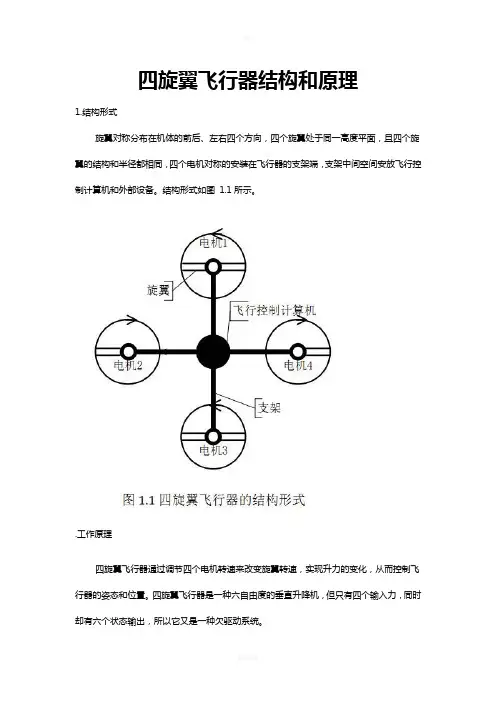
四旋翼飞行器结构和原理1.结构形式旋翼对称分布在机体的前后、左右四个方向,四个旋翼处于同一高度平面,且四个旋翼的结构和半径都相同,四个电机对称的安装在飞行器的支架端,支架中间空间安放飞行控制计算机和外部设备。
结构形式如图1.1所示。
.工作原理四旋翼飞行器通过调节四个电机转速来改变旋翼转速,实现升力的变化,从而控制飞行器的姿态和位置。
四旋翼飞行器是一种六自由度的垂直升降机,但只有四个输入力,同时却有六个状态输出,所以它又是一种欠驱动系统。
四旋翼飞行器的电机1和电机3逆时针旋转的同时,电机2和电机4顺时针旋转,因此当飞行器平衡飞行时,陀螺效应和空气动力扭矩效应均被抵消。
在上图中,电机1和电机3作逆时针旋转,电机2和电机4作顺时针旋转,规定沿x轴正方向运动称为向前运动,箭头在旋翼的运动平面上方表示此电机转速提高,在下方表示此电机转速下降。
(1)垂直运动:同时增加四个电机的输出功率,旋翼转速增加使得总的拉力增大,当总拉力足以克服整机的重量时,四旋翼飞行器便离地垂直上升;反之,同时减小四个电机的输出功率,四旋翼飞行器则垂直下降,直至平衡落地,实现了沿z轴的垂直运动。
当外界扰动量为零时,在旋翼产生的升力等于飞行器的自重时,飞行器便保持悬停状态。
(2)俯仰运动:在图(b)中,电机1的转速上升,电机3 的转速下降(改变量大小应相等),电机2、电机4 的转速保持不变。
由于旋翼1 的升力上升,旋翼3 的升力下降,产生的不平衡力矩使机身绕y 轴旋转,同理,当电机1 的转速下降,电机3的转速上升,机身便绕y轴向另一个方向旋转,实现飞行器的俯仰运动。
(3)滚转运动:与图b 的原理相同,在图c 中,改变电机2和电机4的转速,保持电机1和电机3的转速不变,则可使机身绕x 轴旋转(正向和反向),实现飞行器的滚转运动。
(4)偏航运动:旋翼转动过程中由于空气阻力作用会形成与转动方向相反的反扭矩,为了克服反扭矩影响,可使四个旋翼中的两个正转,两个反转,且对角线上的各个旋翼转动方向相同。

四轴飞行器-概念扫盲最近一个月,在朋友傻鱼的帮助下,搭建起一套四轴飞行器。
鉴于四周飞行器、智能家庭之类的,都是各类Geek蛋疼而毫无创新的爱好,所以给各位分享下其中的一些基本概念。
作为扫盲帖,不含有任何高级内容,内行请直接略过。
先来个照片:首先谈谈四轴的原理,就是4个螺旋桨,对角的两个旋转方向相同,相邻的旋转方向相反。
顺时针转的叫反桨,逆时针转的叫正桨。
所以当他们转速相同时,就可以抵消旋转上带来的反作用力,不至于自己打转。
当然也就不需要直升机的尾桨了。
当然任何东西的制造都有误差,一套四轴飞起来以后,难免各个螺旋桨,机架的平衡等存在些问题。
所以安装后有个很必要的调试的过程,调试以后,过小的误差,就由飞控自己解决了。
也就是确保遥控器没有动作信号时,自己保持平衡。
鉴于四轴的复杂性,没有飞控基本别指望靠手来起飞。
分别讲各个配件吧。
**机架** :就是个架子,用来把各种东西拼上去。
有不同的材料,价格差异也较大。
我买的是SK450,塑料的,比较重,相当的结实,至今没有摔坏。
追求高性能的可以选碳纤维机架的,会轻不少,比如X450、X600。
这里的数字是指轴距,比如SK450和X450的轴距就是450mm。
也就是对角线两个轴之间的距离。
机架上的电机安装座决定了你能安装什么样的电机,轴距决定了最大可以安装多大的桨。
450mm轴距的机架可以安装最大10英寸的桨。
一般初学时买个塑料机架玩玩就好,玩熟悉了可以依据动手能力酌情选择碳纤维或者自己做。
我一开始就是选择这样一个可以尽快飞起来的机架,毕竟系统的迭代要以第一次可运行为基础。
最近开始考虑自己做机架了。
SK450的一个腿的重量就有41克。
而最近发现买IC时带的IC管子,一根20cm的也才不到10克,硬度却是够用的。
105元。
**电机** :这玩意讲究可就多了。
一般玩四轴的也就是22xx 系列的规格。
我用的是朗宇的A2212-KV980。
2212是其尺寸规格,具体我就不列出了。
四轴飞行器是微型飞行器的其中一种,相对于固定翼飞行器,它的方向控制灵活、抗干扰能力强、飞行稳定,能够携带一定的负载和有悬停功能,因此能够很好地进行空中拍摄、监视、侦查等功能,在军事和民用上具备广泛的运用前景。
四轴飞行器关键技术在于控制策略。
由于智能控制算法在运行复杂的浮点型运算以及矩阵运算时,微处理器计算能力受限,难以达到飞行控制实时性的要求;而PID控制简单,易于实现,且技术成熟,因此目前主流的控制策略主要是围绕传统的PID控制展开。
1 四轴飞行器的结构与基本飞行原理四轴飞行器结构主要由主控板和呈十字交叉结构的4个电子调速器、电机、旋浆组成,电机由电子调速器控制,主控板主要负责解算当前飞行姿态、控制电调等功能。
以十字飞行模式为例,l号旋翼为头,1、3号旋翼逆时针旋转,2、4号旋翼顺时针旋转,如图1所示。
图1 四轴飞行器结构图参照飞行状态表1变化电机转速,由于四个电机转速不同,使其与水平面倾斜一定角度,如图l所示。
四个电机产生的合力分解为向上的升力与前向分力。
当重力与升力相等时,前向分力驱动四轴飞行器向倾斜角度的方向水平飞行。
空间三轴角度欧拉角分为仰俯角、横滚角、航向角:倾斜角是仰俯角时,向前、向后飞行;倾斜角是横滚角时,向左、向右飞行;而倾斜航向角时,向左、右旋转运动,左(右)旋转是由于顺时针两电机产生的反扭矩之和与逆时针两电机产生的反扭矩之和不等,即不能相互抵消,机身便在反扭矩作用下绕z轴自旋转。
2 姿态解算四轴飞行器运用姿态解算计算出空间三轴欧拉角。
结构框架如图2所示,陀螺仪采样三轴角速度值,加速度传感器采样三轴加速度值,而磁力传感器采样得到三轴地磁场值,将陀螺仪、加速度传感器、磁力传感器采样后的数据进行标定、滤波、校正后得到三轴欧拉角度,其中陀螺仪和加速度传感器选用MPU6050芯片,磁力传感器选用HMC5883L芯片,采用IIC总线与主控板通信。
图2 姿态解算结构图由于传感器存在器件误差,因此在使用前需要标定。
四轴飞行器飞控原理四轴飞行器飞控原理 (1)一、六种姿态控制原理示意 (3)二、四轴翼飞行器系统建模 (4)2.1假设条件: (4)2.2建立坐标系: (5)2.3转换矩阵推导: (6)2.4非线性模型 (7)2.5模型线性化 (11)三、基于PID的飞行控制 (15)四、硬件设计与实现 (17)4.1四轴飞行器硬件电路 (17)五、国内外四轴飞行器 (17)5.1 Kesterl (17)5.2 Unav3500 (18)5.3 MikroKoper (18)5.4 ArduPilot (19)5.5 Crazyflie (20)一、六种姿态控制原理示意图1 上下(高度)控制,就是四个螺旋桨同时增加(减小)转速;图2 前进、后退图3 左飞、右飞图4 类似打方向盘,改变航向二、四轴翼飞行器系统建模2.1假设条件:微小型四旋翼飞行器在三维空间中可视为刚体,飞行器在空间中的运动具有六个自由度,即飞行器质心在空间中的三个平移自由度和三个旋转自由度。
由于该飞行器一般为低空低速飞行,因此可以对其动力学模型的建立做如下假设:1)微小型四旋翼飞行器在研究中视为刚体,忽略其弹性影响,总质量m 为常数;2)将地球视为惯性系统,忽略地球自转和公转对飞行器的影响;3)假设地面为水平平面,忽略地球曲率的影响;4)重力加速度g为常数,不随地理位置和飞行高度的变化而变化;5)飞行器机机体几何外形完全对称且质量分布均勻,质心与几何中心重合。
2.2建立坐标系:图5机体坐标系B、地面坐标系EФ绕X轴方向的横滚角(rad);θ绕轴方向的俯仰角(rad);ψ绕Z轴方向的偏航角(rad):2.3转换矩阵推导:(可以查阅高等数学方向余弦,矩阵论中的旋转矩阵等资料)公式(1)公式(2)2.4非线性模型由于作用到飞行器上的合力和合力矩是四个螺旋奖所产生的力与力矩的矢量和,因此,他们之间存在极大地交叉耦合特性。
例如,横滚(俯仰)力矩的改变将会对侧向(纵向)加速度有一个直接的影响。
BK2425Low Power High Performance 2.4 GHz GFSK Transceiver Features Pin Assignments⏹2400-2483.5 MHz ISM band operation⏹Support 250Kbps, 1Mbps and 2 Mbps airdata rate⏹Programmable output power⏹Low power consumption⏹Tolerate +/- 60ppm 16 MHz crystal⏹Variable payload length from 1 to 32bytes⏹Automatic packet processing⏹ 6 data pipes for 1:6 star networks⏹ 1.9V to 3.6V power supply⏹4-pin SPI interface with maximum 8 MHzclock rate⏹20-pin 4x4mm QFN packageApplications⏹Wireless PC peripherals⏹Wireless gamepads⏹Wireless audio⏹Remote controls⏹Home automation⏹ToysBlock DiagramNC CDVDD VDD VSS VDD20 19 18 17 16CE 1 15 VDDCSN 2 14 VSSSCKBK2425 RF3 13MOSI 4 12 NCMISO 5 11 NC6 7 8 9 10IRQ NC NC XO XI四轴飞行器遥控硬件+全套源代码 + 飞控Arm Cortex 硬件原理图PCB 联系:QQ 766384919RFPFMData SlicerRx FIFOInterfaceSPICSN RFN SCKDemodulatorMOSIMISOIntegratedPowerPacketIRQ TDD RF Processing &ManagementTransceiver State Control CEFM ModulatorGaussianbanksRegistershaping Tx FIFOXTALP XTALNRevision 1.0 Copyright © 2013 Beken Corporation Jan, 2013 Page 1 of 30BK2425 Table of Contents1 General Description (3)2 Abbreviations (4)3 Pin Information (5)4 State Control (6)4.1 State Control Diagram (6)4.2 Power Down Mode (7)4.3 Standby-I Mode (7)4.4 Standby-II Mode (7)4.5 TX Mode (7)4.6 RX Mode (8)5 Packet Processing (8)5.1 Packet Format (8)5.1.1 Preamble (9)5.1.2 Address (9)5.1.3 Packet Control (9)5.1.4 Payload (10)5.1.5 CRC (10)5.2 Packet Handling (10)6 Data and Control Interface (11)6.1 TX/RX FIFO (11)6.2 Interrupt (11)6.3 SPI Interface (12)6.3.1 SPI Command (12)6.3.2 SPI Timing (13)7 Register Map (15)7.1 Register Bank 0 (15)7.2 Register Bank 1 (21)8 Electrical Specifications (22)9 Typical Application Schematic (23)10 Package and Die Bonding Information (24)10.1 Package Information (24)10.2 Die Bonding Information (25)10.3 PCB Bonding diagram (27)11 Order Information (28)12 Contact Information (29)13 Update History (30)BK2425 1 General DescriptionBK2425 is a GFSK transceiver operating in theworld wide ISM frequency band at 2400-2483.5 MHz. Burst mode transmission and upto 2Mbps air data rate make them suitable forapplications requiring ultra low powerconsumption. The embedded packet processingengines enable their full operation with a verysimple MCU as a radio system. Auto re-transmission and auto acknowledge givereliable link without any MCU interference.BK2425 operates in TDD mode, either as atransmitter or as a receiver.The RF channel frequency determines thecenter of the channel used by BK2425. Thefrequency is set by the RF_CH register inregister bank 0 according to the followingformula: F0= 2400 + RF_CH (MHz). Theresolution of the RF channel frequency is1MHz.A transmitter and a receiver must beprogrammed with the same RF channelfrequency to be able to communicate with eachother.The output power of BK2425 is set by theRF_PWR bits in the RF_SETUP register.Demodulation is done with embedded dataslicer and bit recovery logic. The air data ratecan be programmed to 250Kbps, 1Mbps or2Mbps by RF_DR_HIGH and RF_DR_LOWregister. A transmitter and a receiver must beprogrammed with the same setting.In the following chapters, all registers are inregister bank 0 except with explicit claim.RFPFMData SlicerRx FIFOInterfaceSPICSN RFN SCKDemodulatorMOSIMISOIntegratedPowerPacketIRQ TDD RF Processing &ManagementTransceiver State Control CEFM ModulatorGaussianbanksRegistershaping Tx FIFOXTALP XTALNFigure 1 BK2425 Chip Block DiagramBK2425 2 AbbreviationsACK AcknowledgementARC Auto Retransmission CountARD Auto Retransmission DelayCD Carrier DetectionCE Chip EnableCRC Cyclic Redundancy CheckCSN Chip Select NotDPL Dynamic Payload LengthFIFO First-In-First-OutGFSK Gaussian Frequency Shift KeyingGHz GigahertzLNA Low Noise AmplifierIRQ Interrupt RequestISM Industrial-Scientific-MedicalLSB Least Significant BitMAX_RT Maximum RetransmitMbps Megabit per secondMCU Microcontroller UnitMHz MegahertzMISO Master In Slave OutMOSI Master Out Slave InMSB Most Significant BitPA Power AmplifierPID Packet Identity BitsPLD PayloadPRX Primary RXPTX Primary TXPWD_DWN Power DownPWD_UP Power UpRF_CH Radio Frequency ChannelRSSI Received Signal Strength IndicatorRX ReceiveRX_DR Receive Data ReadySCK SPI ClockSPI Serial Peripheral InterfaceTDD Time Division DuplexTX TransmitTX_DS Transmit Data SentXTAL CrystalBK2425 3 Pin InformationNC CDVDD VDD VSS VDD20 19 18 17 16CE 1 15 VDDCSN 2 14 VSSBK2425 RFSCK 3 13MOSI 4 12 NCMISO 5 11 NC6 7 8 9 10IRQ NC NC XO XIFigure 2 BK2425 pin assignments (top view) for the QFN20 packagePIN Name Pin Function Description1 CE Digital Input Chip Enable Activates RX or TX mode2 CSN Digital Input SPI Chip Select, Active low3 SCK Digital Input SPI Clock4 MOSI Digital Input SPI Slave Data Input5 MISO Digital Output SPI Slave Data Output with tri-state option6 IRQ Digital Output Maskable interrupt pin, Active low7 NC No Connection8 NC No Connection9 XO Analog Output Crystal oscillator, node P (inverter output)10 XI Analog Input Crystal oscillator, node N (inverter input)11 NC No Connection12 NC No Connection13 RFN RF port RF output (PA) /Input (LNA), port N.14 VSS Ground Ground (0 V)15 VDD Power Power Supply (1.9 V to 3.6 V DC)16 VDD Power Supply (1.9 V to 3.6 V DC)17 VSS Ground Ground (0 V)18 VDD Power Power Supply (1.9 V to 3.6 V DC)19 CDVDD Analog Output Digital regulator output decoupling capacitor20 NC No ConnectionTable 1 BK2425 QFN20 pin functionsRevision 1.0Proprietary and Confidential Page 5 of 30BK24254 State Control4.1 State Control Diagram⏹ Pin signal: VDD, CE⏹ SPI register: PWR_UP, PRIM_RX, EN_AA, NO_ACK, ARC, ARD⏹System information: Time out, ACK received, ARD elapsed, ARC_CNT, TX FIFO empty, ACK packet transmitted, Packet receivedBK2425 has built-in state machines that control the state transition between different modes.When auto acknowledge feature is disabled, state transition will be fully controlled by MCU.Figure 3 PTX (PRIM_RX=0) state control diagramBK2425Figure 4 PRX (PRIM_RX=1) state control diagram4.2 Power Down ModeIn power down mode BK2425 is in sleep mode with minimal current consumption. SPI interface is still active in this mode, and all register values are available by SPI. Power down mode is entered by setting the PWR_UP bit in the CONFIG register to low.4.3 Standby-I ModeBy setting the PWR_UP bit in the CONFIG register to 1 and de-asserting CE to 0, the device enters standby-I mode. Standby-I mode is used to minimize average current consumption while maintaining short start-up time. In this mode, part of the crystal oscillator is active. This is also the mode which the BK2425 returns to from TX or RX mode when CE is set low.4.4 Standby-II ModeIn standby -II mode more clock buffers are active than in standby-I mode and much more current is used. Standby-II occurs when CE is held high on a PTX device with empty TX FIFO. If a new packet is uploaded to the TX FIFO in this mode, the device will automatically enter TX mode and the packet is transmitted.4.5 TX Mode⏹ PTX device (PRIM_RX=0)The TX mode is an active mode where the PTX device transmits a packet. To enter this mode from power down mode, the PTX device must have the PWR_UP bit set high, PRIM_RX bit set low, a payload in the TX FIFO, and a high pulse on the CE for more than 10µs.BK2425The PTX device stays in TX mode until it finishes transmitting the current packet. If CE = 0 it returns to standby-I mode. If CE = 1, the next action is determined by the status of the TX FIFO. If the TX FIFO is not empty the PTX device remains in TX mode, transmitting the next packet. If the TX FIFO is empty the PTX device goes into standby-II mode. It is important to never stay in TX mode for more than 4ms at one time.If the auto retransmit is enabled (EN_AA=1) and auto acknowledge is required (NO_ACK=0), the PTX device will enter TX mode from standby-I mode when ARD elapsed and number of retried is less than ARC.⏹ PRX device (PRIM_RX=1)The PRX device will enter TX mode from RX mode only when EN_AA=1 and NO_ACK=0 in received packet to transmit acknowledge packet with pending payload in TX FIFO.4.6 RX Mode⏹ PRX device (PRIM_RX=1)The RX mode is an active mode where the BK2425 radio is configured to be a receiver. To enter this mode from standby-I mode, the PRX device must have the PWR_UP bit set5 Packet Processinghigh, PRIM_RX bit set high and the CE pin set high. Or PRX device can enter this mode from TX mode after transmitting an acknowledge packet when EN_AA=1 and NO_ACK=0 in received packet.In this mode the receiver demodulates the signals from the RF channel, constantly presenting the demodulated data to the packet processing engine. The packet processing engine continuously searches for a valid packet. If a valid packet is found (by a matching address and a valid CRC) the payload of the packet is presented in a vacant slot in the RX FIFO. If the RX FIFO is full, the received packet is discarded.The PRX device remains in RX mode until the MCU configures it to standby-I mode or power down mode.In RX mode a carrier detection (CD) signal is available. The CD is set to high when a RF signal is detected inside the receiving frequency channel. The internal CD signal is filtered before presented to CD register. The RF signal must be present for at least 128 µs before the CD is set high.⏹ PTX device (PRIM_RX=0)The PTX device will enter RX mode from TX mode only when EN_AA=1 and NO_ACK=0 to receive acknowledge packet.5.1 Packet FormatThe packet format has a preamble, address, packet control, payload and CRC field.Preamble 1 byteAddress 3~5 byte Packet Control 9/0 bit Payload 0~32 byte CRC 2/1 bytePayload Length 6 bitPID 2 bitNO_ACK 1 bitFigure 5 Packet FormatBK24255.1.1PreambleThe preamble is a bit sequence used to detect 0 and 1 levels in the receiver. The preamble is one byte long and is either 01010101 or 10101010. If the first bit in the address is 1 the preamble is automatically set to 10101010 and if the first bit is 0 the preamble is automatically set to 01010101. This is done to ensure there are enough transitions in the preamble to stabilize the receiver.5.1.2AddressThis is the address for the receiver. An address ensures that the packet is detected by the target receiver. The address field can be configured to be 3, 4, or 5 bytes long by the AW register.The PRX device can open up to six data pipes to support up to six PTX devices with unique addresses. All six PTX device addresses are searched simultaneously. In PRX side, the data pipes are enabled with the bits in the EN_RXADDR register. By default only data pipe 0 and 1 are enabled.Each data pipe address is configured in the RX_ADDR_PX registers.Each pipe can have up to 5 bytes configurable address. Data pipe 0 has a unique 5 byte address. Data pipes 1-5 share the 4 most significant address bytes. The LSB byte must be unique for all 6 pipes.To ensure that the ACK packet from the PRX is transmitted to the correct PTX, the PRX takes the data pipe address where it received the packet and uses it as the TX address when transmitting the ACK packet.On the PRX, the RX_ADDR_Pn, defined as the pipe address, must be unique. On the PTX the TX_ADDR must be the same as the RX_ADDR_P0 on the PTX, and as the pipe address for the designated pipe on the PRX. No other data pipe can receive data until a complete packet is received by a data pipe that has detected its address. When multiple PTX devices are transmitting to a PRX, the ARD can be used to skew the auto retransmission so that they only block each other once.5.1.3Packet ControlWhen Dynamic Payload Length function is enabled, the packet control field contains a 6 bit payload length field, a 2 bit PID (Packet Identity) field and, a 1 bit NO_ACK flag.⏹Payload lengthThe payload length field is only used if the Dynamic Payload Length function is enabled.⏹PIDThe 2 bit PID field is used to detect whether the received packet is new or retransmitted. PID prevents the PRX device from presenting the same payload more than once to the MCU. The PID field is incremented at the TX side for each new packet received through the SPI. The PID and CRC fields are used by the PRX device to determine whether a packet is old or new. When several data packets are lost on the link, the PID fields may become equal to the last received PID. If a packet has the same PID as the previous packet, BK2425 compares the CRC sums from both packets. If the CRC sums are also equal, the last received packet is considered a copy of the previously received packet and discarded.⏹NO_ACKThe NO_ACK flag is only used when the auto acknowledgement feature is used. Setting the flag high, tells the receiver that the packet is not to be auto acknowledged.The PTX can set the NO_ACK flag bit in the Packet Control Field with the command: W_TX_PAYLOAD_NOACK. However, the function must first be enabled in the FEATURE register by setting theRevision 1.0Proprietary and Confidential Page 9 of 30BK2425EN_DYN_ACK bit. When you use this option, the PTX goes directly to standby-I mode after transmitting the packet and the PRX does not transmit an ACK packet when it receives the packet.5.1.4PayloadThe payload is the user defined content of the packet. It can be 0 to 32 bytes wide, and it is transmitted on-air as it is uploaded (unmodified) to the device.The BK2425 provides two alternatives for handling payload lengths, static and dynamic payload length. The static payload length of each of six data pipes can be individually set. The default alternative is static payload length. With static payload length all packets between a transmitter and a receiver have the same length. Static payload length is set by the RX_PW_Px registers. The payload length on the transmitter side is set by the number of bytes clocked into the TX_FIFO and must equal the value in the RX_PW_Px register on the receiver side. Each pipe has its own payload length.Dynamic Payload Length (DPL) is an alternative to static payload length. DPL enables the transmitter to send packets with variable payload length to the receiver. This means for a system with different payload lengths it is not necessary to scale the packet length to the longest payload.With DPL feature the BK2425 can decode the payload length of the received packet automatically instead of using the RX_PW_Px registers. The MCU can read the length of the received payload by using the command: R_RX_PL_WID.In order to enable DPL the EN_DPL bit in the FEATURE register must be set. In RX mode the DYNPD register has to be set. A PTX that transmits to a PRX with DPL enabled must have the DPL_P0 bit in DYNPD set. 5.1.5CRCThe CRC is the error detection mechanism in the packet. The number of bytes in the CRC is set by the CRCO bit in the CONFIG register. It may be either 1 or 2 bytes and is calculated over the address, Packet Control Field, and Payload.The polynomial for 1 byte CRC is X8 + X2 + X + 1. Initial value is 0xFF.The polynomial for 2 byte CRC is X16 + X12 + X5 + 1. Initial value is 0xFFFF.No packet is accepted by receiver side if the CRC fails.5.2Packet HandlingBK2425 uses burst mode for payload transmission and receive.The transmitter fetches payload from TX FIFO, automatically assembles it into packet and transmits the packet in a very short burst period with 1Mbps or 2Mbps air data rate.After transmission, if the PTX packet has the NO_ACK flag set, BK2425 sets TX_DS and gives an active low interrupt IRQ to MCU. If the PTX is ACK packet, the PTX needs receive ACK from the PRX and then asserts the TX_DS IRQ.The receiver automatically validates and disassembles received packet, if there is a valid packet within the new payload, it will write the payload into RX FIFO, set RX_DR and give an active low interrupt IRQ to MCU.When auto acknowledge is enabled (EN_AA=1), the PTX device will automatically wait for acknowledge packet after transmission, and re- transmit original packet with the delay of ARD until an acknowledge packet is received or the number of re-transmission exceeds a threshold ARC. If the later one happens, BK2425 will set MAX_RT and give an active low interruptRevision 1.0Proprietary and Confidential Page 10 of 30BK2425IRQ to MCU. Two packet loss counters (ARC_CNT and PLOS_CNT) are incremented each time a packet is lost. The ARC_CNT counts the number of retransmissions for the current transaction. The PLOS_CNT counts the total number of retransmissions since the last channel change. ARC_CNT is reset by initiating a new transaction. PLOS_CNT is reset by writing to the RF_CH register. It is possible to use the information in the OBSERVE _TX register to make an overall assessment of the channel quality.The PTX device will retransmit if its RX FIFO is full but received ACK frame has payload.As an alternative for PTX device to auto retransmit it is possible to manually set the BK2425 to retransmit a packet a number of times. This is done by the REUSE_TX_PL command.When auto acknowledge is enabled, the PRX device will automatically check the NO_ACK field in received packet, and if NO_ACK=0, it will automatically send an acknowledge packet to PTX device. If EN_ACK_PAY is set, and the acknowledge packet can also include pending payload in TX FIFO.6 Data and Control Interface 6.1TX/RX FIFOThe data FIFOs are used to store payload that is to be transmitted (TX FIFO) or payload that is received and ready to be clocked out (RX FIFO). The FIFO is accessible in both PTX mode and PRX mode.There are three levels 32 bytes FIFO for both TX and RX, supporting both acknowledge mode or no acknowledge mode with up to six pipes.⏹TX three levels, 32 byte FIFO⏹RX three levels, 32 byte FIFOBoth FIFOs have a controller and are accessible through the SPI by using dedicated SPI commands. A TX FIFO in PRX can store payload for ACK packets to three different PTX devices. If the TX FIFO contains more than one payload to a pipe, payloads are handled using the first in first out principle. The TX FIFO in a PRX is blocked if all pending payloads are addressed to pipes where the link to the PTX is lost. In this case, the MCU can flush the TX FIFO by using the FLUSH_TX command.The RX FIFO in PRX may contain payload from up to three different PTX devices.A TX FIFO in PTX can have up to three payloads stored.The TX FIFO can be written to by three commands, W_TX_PAYLOAD and W_ TX_PAYLOAD_NO_ACK in PTX mode and W_ACK_PAYLOAD in PRX mode. All three commands give access to the TX_PLD register. The RX FIFO can be read by the command R_RX _PAYLOAD in both PTX and PRX mode. This command gives access to the RX_PLD register.The payload in TX FIFO in a PTX is NOT removed if the MAX_RT IRQ is asserted.In the FIFO_STATUS register it is possible to read if the TX and RX FIFO are full or empty. The TX_REUSE bit is also available in the FIFO_STATUS register. TX_REUSE is set by the SPI command REUSE_TX_PL, and is reset by the SPI command: W_TX_PAYLOAD or FLUSH TX.6.2InterruptIn BK2425 there is an active low interrupt (IRQ) pin, which is activated when TX_ DS IRQ, RX_DR IRQ or MAX_RT IRQ are set high by the state machine in the STATUS register. The IRQ pin resets when MCU writes '1' to the IRQ source bit in the STATUS register. The IRQ mask in the CONFIGRevision 1.0Proprietary and Confidential Page 11 of 30BK2425register is used to select the IRQ sources that are allowed to assert the IRQ pin. By setting one of the MASK bits high, the corresponding IRQ source is disabled. By default all IRQ sources are enabled.The 3 bit pipe information in the STATUS register is updated during the IRQ pin high to low transition. If the STATUS register is read during an IRQ pin high to low transition, the pipe information is unreliable.6.3SPI Interface6.3.1SPI CommandThe SPI commands are shown in Table 3. Every new command must be started by a high to low transition on CSN.In parallel to the SPI command word applied on the MOSI pin, the STATUS register is shifted serially out on the MISO pin.The serial shifting SPI commands is in the following format:⏹<Command word: MSB bit to LSB bit(one byte)>⏹<Data bytes: LSB byte to MSB byte, MSBbit in each byte first> for all registers atbank 0 and register 9 to register 14 at bank1⏹<Data bytes: MSB byte to LSB byte, MSBbit in each byte first> for register 0 toregister 8 at bank 1Command# DataOperation Command name wordbytes(binary)R_REGISTER 000A AAAA 1 to 5 Read command and status registers. AAAAA = LSB byte first 5 bit Register Map Address1 to 5Write command and status registers. AAAAA = 5W_REGISTER 001A AAAA bit Register Map AddressLSB byte first Executable in power down or standby modes only.1 to 32 Read RX-payload: 1 – 32 bytes. A read operationR_RX_PAYLOAD 0110 0001 always starts at byte 0. Payload is deleted from FIFOLSB byte first after it is read. Used in RX mode.W_TX_PAYLOAD 1010 0000 1 to 32 Write TX-payload: 1 – 32 bytes. A write operation LSB byte first always starts at byte 0 used in TX payload.FLUSH_TX 1110 0001 0 Flush TX FIFO, used in TX modeFlush RX FIFO, used in RX modeFLUSH_RX 1110 0010 0 Should not be executed during transmission of acknowledge, that is, acknowledge package will not be completed.Used for a PTX deviceReuse last transmitted payload. Packets are repeatedly retransmitted as long as CE is high.REUSE_TX_PL 1110 0011 0 TX payload reuse is active untilW_TX_PAYLOAD or FLUSH TX is executed. TX payload reuse must not be activated or deactivated during package transmissionRevision 1.0Proprietary and Confidential Page 12 of 30BK2425 This write command followed by data 0x73 activates the following features:• R_RX_PL_WID• W_ACK_PAYLOAD• W_TX_PAYLOAD_NOACKA new ACTIVATE command with the same data deactivates them again. This is executable in power down or stand by modes only.ACTIVATE 0101 0000 1 The R_RX_PL_WID, W_ACK_PAYLOAD, andW_TX_PAYLOAD_NOACK features registers are initially in a deactivated state; a write has no effect, a read only results in zeros on MISO. To activate these registers, use the ACTIVATE command followed by data 0x73. Then they can be accessed as any other register. Use the same command and data to deactivate the registers again.This write command followed by data 0x53 toggles the register bank, and the current register bank number can be read out from REG7 [7]R_RX_PL_WID 0110 0000 Read RX-payload width for the topR_RX_PAYLOAD in the RX FIFO.Used in RX mode.Write Payload to be transmitted together with ACK packet on PIPE PPP. (PPP valid in the rangeW_ACK_PAYLOAD 1010 1PPP 1 to 32 from 000 to 101). Maximum three ACK packetLSB byte first payloads can be pending. Payloads with same PPP are handled using first in - first out principle. Writepayload: 1– 32 bytes. A write operation always startsat byte 0.W_TX_PAYLOAD_NO1011 0000 1 to 32 Used in TX mode. Disables AUTOACK on thisACK LSB byte first specific packet.NOP 1111 1111 0 No Operation. Might be used to read the STATUS registerTable 2 SPI command6.3.2SPI TimingS C KC S NW r i t e t o S P I r e g i s t e r:M O S I x C 7 C 6 C 5 C 4 C 3 C 2 C 1 C 0 x D 7 D 6 D 5 D 4 D 3 D 2 D 1 D 0 x M I S O H I - Z S 7 S 6 S 5 S 4 S 3 S 2 S 1 S 0 0 0 0 0 0 0 0 0 H i - Z R e a d f r o m S P I r e g i s t e r:M O S I x C 7 C 6 C 5 C 4 C 3 C 2 C 1 C 0 xM I S O x S 7 S 6 S 5 S 4 S 3 S 2 S 1 S 0 D 7 D 6 D 5 D 4 D 3 D 2 D 1 D 0 xFigure 6 SPI timingRevision 1.0Proprietary and Confidential Page 13 of 30BK2425 Cn: SPI command bitSn: STATUS register bitDn: Data Bit (LSB byte to MSB byte, MSB bit in each byte first)Note: The SPI timing is for bank 0 and register 9 to 14 at bank 1. For register 0 to 8 at bank 1, the byte order is inversed that the MSB byte is R/W before LSB byte.Figure 7 SPI NOP timing diagramSymbol Parameters Min Max UnitsTdc Data to SCK Setup 10 nsTdh SCK to Data Hold 20 nsTcsd CSN to Data Valid 38 nsTcd SCK to Data Valid 55 nsTcl SCK Low Time 40 nsTch SCK High Time 40 nsFsck SCK Frequency 0 8 MHzTr,Tf SCK Rise and Fall 100 nsTcc CSN to SCK Setup 2 nsTcch SCK to CSN Hold 2 nsTcwh CSN Inactive time 50 nsTcdz CSN to Output High Z 38 nsTable 3 SPI timing parameterRevision 1.0Proprietary and Confidential Page 14 of 30BK24257 Register MapThere are two register banks, which can be toggled by SPI command “ACTIVATE” followed with0x53 byte, and bank status can be read from Bank0_REG7 [7].7.1Register Bank 0AddressMnemonic Bit ResetType Description(Hex) Value00 CONFIG Configuration RegisterReserved 7 0 R/W Only '0' allowedMASK_RX_DR 6 0 R/W Mask interrupt caused by RX_DR1: Interrupt not reflected on the IRQ pin0: Reflect RX_DR as active low interrupton the IRQ pinMASK_TX_DS 5 0 R/W Mask interrupt caused by TX_DS1: Interrupt not reflected on the IRQ pin0: Reflect TX_DS as active low interrupton the IRQ pinMASK_MAX_RT 4 0 R/W Mask interrupt caused by MAX_RT1: Interrupt not reflected on the IRQ pin0: Reflect MAX_RT as active lowinterrupt on the IRQ pinEN_CRC 3 1 R/W Enable CRC. Forced high if one of the bits in the EN_AA is highCRCO 2 0 R/W CRC encoding scheme'0' - 1 byte'1' - 2 bytesPWR_UP 1 0 R/W 1: POWER UP, 0:POWER DOWNPRIM_RX 0 0 R/W RX/TX control,1: PRX, 0: PTX01 EN_AA Enable ‘Auto Acknowledgment’ FunctionReserved 7:6 00 R/W Only '00' allowedENAA_P5 5 1 R/W Enable auto acknowledgement data pipe 5ENAA_P4 4 1 R/W Enable auto acknowledgement data pipe 4ENAA_P3 3 1 R/W Enable auto acknowledgement data pipe 3ENAA_P2 2 1 R/W Enable auto acknowledgement data pipe 2ENAA_P1 1 1 R/W Enable auto acknowledgement data pipe 1ENAA_P0 0 1 R/W Enable auto acknowledgement data pipe 0 02 EN_RXADDR Enabled RX AddressesReserved 7:6 00 R/W Only '00' allowedERX_P5 5 0 R/W Enable data pipe 5.ERX_P4 4 0 R/W Enable data pipe 4.ERX_P3 3 0 R/W Enable data pipe 3.ERX_P2 2 0 R/W Enable data pipe 2.ERX_P1 1 1 R/W Enable data pipe 1.ERX_P0 0 1 R/W Enable data pipe 0.Revision 1.0 Proprietary and Confidential Page 15 of 30BK2425 03 SETUP_AW Setup of Address Widths(common for all data pipes)Reserved 7:2 000000 R/W Only '000000' allowedAW 1:0 11 R/W RX/TX Address field width'00' - Illegal'01' - 3 bytes'10' - 4 bytes'11' - 5 bytesLSB bytes are used if address width is below 5 bytes04 SETUP_RETR Setup of Automatic RetransmissionARD 7:4 0000 R/W Auto Retransmission Delay‘0000’ – Wait 250 us‘0001’ – Wait 500 us‘0010’ – Wait 750 us……..‘1111’ – Wait 4000 us(Delay defined from end of transmission tostart of next transmission)ARC 3:0 0011 R/W Auto Retransmission Count‘0000’ –Re-Transmit disabled‘0001’ – Up to 1 Re-Transmission on fail of AA……‘1111’ – Up to 15 Re-Transmission on fail of AA05 RF_CH RF ChannelReserved 7 0 R/W Only '0' allowedRF_CH 6:0 0000010 R/W Sets the frequency channel 06 RF_SETUP RF Setup RegisterReserved 7:6 0 R/W Only '00' allowedRF_DR_LOW 5 0 R/W Set Air Data Rate. See RF_DR_HIGH for encoding.PLL_LOCK 4 0 R/W Force PLL lock signal. Only used in testSet Air Data Rate.RF_DR_HIGH 3 1 R/W Encoding: RF_DR_LOW, RF_DR_HIGH: ‘00’ – 1Mbps‘01’ – 2Mbps (default)‘10’ – 250Kbps‘11’ – 2MbpsRF_PWR[1:0] 2:1Set RF output power in TX mode 11 R/W RF_PWR[1:0]Setup LNA gainLNA_HCURR 0 1 R/W 0:Low gain(20dB down)1:High gainStatus Register (In parallel to the SPI07 STATUS command word applied on the MOSI pin,the STATUS register is shifted serially outon the MISO pin)Register bank selection states. SwitchRBANK 7 0 R register bank is done by SPI command “ACTIVATE” followed by 0x530: Register bank 0。
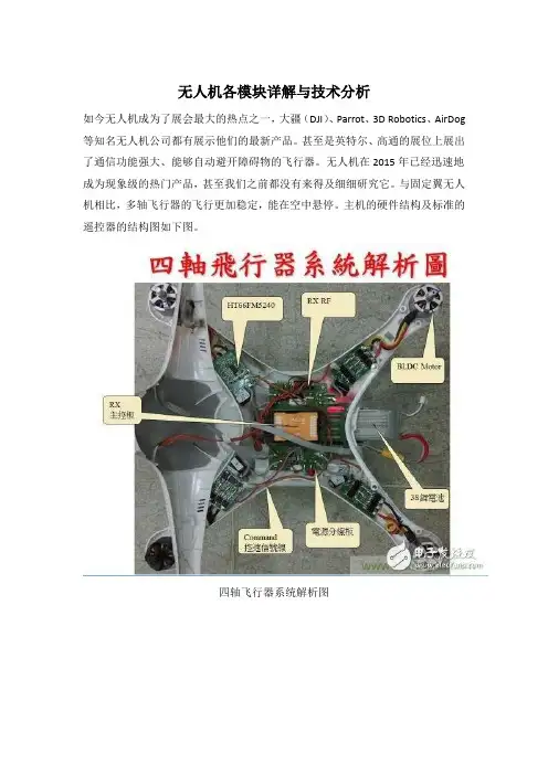
无人机各模块详解与技术分析如今无人机成为了展会最大的热点之一,大疆(DJI)、Parrot、3D Robotics、AirDog 等知名无人机公司都有展示他们的最新产品。
甚至是英特尔、高通的展位上展出了通信功能强大、能够自动避开障碍物的飞行器。
无人机在2015年已经迅速地成为现象级的热门产品,甚至我们之前都没有来得及细细研究它。
与固定翼无人机相比,多轴飞行器的飞行更加稳定,能在空中悬停。
主机的硬件结构及标准的遥控器的结构图如下图。
四轴飞行器系统解析图遥控器系统解析图以上只是标准产品的解剖图,有些更加高级的如针对航模发烧友和航拍用户们的无人机系统,还会要求有云台、摄像头、视频传输系统以及视频接收等更多模块。
飞控的大脑:微控制器在四轴飞行器的飞控主板上,需要用到的芯片并不多。
目前的玩具级飞行器还只是简单地在空中飞行或停留,只要能够接收到遥控器发送过来的指令,控制四个马达带动桨翼,基本上就可以实现飞行或悬停的功能。
意法半导体高级市场工程师介绍,无人机/多轴飞行器主要部件包括飞行控制以及遥控器两部分。
其中飞行控制包括电调/马达控制、飞机姿态控制以及云台控制等。
目前主流的电调控制方式主要分成BLDC方波控制以及FOC正弦波控制。
新唐的MCU负责人表示:多轴飞行器由遥控,飞控,动力系统,航拍等不同模块构成,根据不同等级产品的需求,会采用到不同CPU内核。
例如小四轴的飞行主控,因功能单纯,体积小,必须同时整合遥控接收,飞行控制及动力驱动功能;中高阶多轴飞行器则采用内建DSP 及浮点运算单元的,负责飞行主控功能,驱动无刷电机的电调(ESC)板则采用MINI5($1.0889)系列设计。
低阶遥控器使用SOP20 封装的4T 8051 N79E814;中高阶遥控器则采用Cortex-M0 M051系列。
另外,内建ARM9及H.264视频边译码器的N329系列SOC则应用于2.4G 及5.8G的航拍系统。
在飞控主板上,目前控制和处理用得最多的还是MCU而不是CPU。

四轴四轴(1)-飞行原理总算能抽出时间写下四轴文章,算算接触四轴也两年多了,从当初的模仿到现在的自主创作经历了不少收获了也不少。
朋友们也经常问我四轴怎么入门,今天就简单写下四轴入门的基本知识。
尽量避开专业术语和数学公式。
1、首先先了解下四轴的飞行原理。
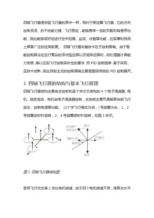
四轴的一般结构都是十字架型,当然也有其他奇葩结构,比如工字型。
两种的力学模型稍微有些不一样,建议先从常规结构入手(其实是其他结构我不懂)。
常规十字型结构其他结构常规结构的力学模型如图。
力学模型对四轴进行受力分析,其受重力、螺旋桨的升力,螺旋桨旋转给机体的反扭矩力。
反扭矩影响主要是使机体自旋,可以想象一下直升机没有尾桨的情况。
螺旋桨旋转时产生的力很复杂,这里将其简化成只受一个升力和反扭矩力。
其它力暂时先不管,对于目前建模精度还不需要分析其他力,顶多在需要时将其他力设为干扰就可以了。
如需对螺旋桨受力进行详细研究可以看些空气动力学的书,推荐两本,空气螺旋桨理论及其应用(刘沛清,北航出版社)空气动力学基础上下册(徐华舫,国防科技大学)网易公开课:这个比麻省理工的那个飞行器构造更对口一些。
荷兰代尔夫特理工大学公开课:空气动力学概论以上这些我是没看下去,太难太多了,如想刨根问底可以看看。
解释下反扭矩的产生:电机带动螺旋桨旋转,比如使螺旋桨顺时针旋转,那么电机就要给螺旋桨一个顺时针方向的扭矩(数学上扭矩的方向不是这样定义的,可以根据右手定则来确定方向)。
根据作用力与反作用力关系,螺旋桨必然会给电机一个反扭矩。
在转速恒定,真空,无能量损耗时,螺旋桨不需要外力也能保持恒定转速,这样也就不存在扭矩了,当然没有空气也飞不起来了。
反扭矩的大小主要与介质密度有关,同样转速在水中的反扭矩肯定比空气中大。
因为存在反扭矩,所以四轴设计成正反桨模式,两个正桨顺时针旋转,两个反桨逆时针旋转,对角桨类型一样,产生的反扭矩刚好相互抵消。
并且还能保持升力向上。
六轴、八轴…类似。
我们控制四轴就是通过控制4个升力和4个反扭矩来控制四轴姿态。
四轴飞行器飞控原理四轴飞行器飞控原理 (1)一、六种姿态控制原理示意 (3)二、四轴翼飞行器系统建模 (4)2.1假设条件: (4)2.2建立坐标系: (5)2.3转换矩阵推导: (6)2.4非线性模型 (7)2.5模型线性化 (11)三、基于PID的飞行控制 (15)四、硬件设计与实现 (17)4.1四轴飞行器硬件电路 (17)五、国内外四轴飞行器 (17)5.1 Kesterl (17)5.2 Unav3500 (18)5.3 MikroKoper (18)5.4 ArduPilot (19)5.5 Crazyflie (20)一、六种姿态控制原理示意图1 上下(高度)控制,就是四个螺旋桨同时增加(减小)转速;图2 前进、后退图3 左飞、右飞图4 类似打方向盘,改变航向二、四轴翼飞行器系统建模2.1假设条件:微小型四旋翼飞行器在三维空间中可视为刚体,飞行器在空间中的运动具有六个自由度,即飞行器质心在空间中的三个平移自由度和三个旋转自由度。
由于该飞行器一般为低空低速飞行,因此可以对其动力学模型的建立做如下假设:1)微小型四旋翼飞行器在研究中视为刚体,忽略其弹性影响,总质量m 为常数;2)将地球视为惯性系统,忽略地球自转和公转对飞行器的影响;3)假设地面为水平平面,忽略地球曲率的影响;4)重力加速度g为常数,不随地理位置和飞行高度的变化而变化;5)飞行器机机体几何外形完全对称且质量分布均勻,质心与几何中心重合。
2.2建立坐标系:图5机体坐标系B、地面坐标系EФ绕X轴方向的横滚角(rad);θ绕轴方向的俯仰角(rad);ψ绕Z轴方向的偏航角(rad):2.3转换矩阵推导:(可以查阅高等数学方向余弦,矩阵论中的旋转矩阵等资料)公式(1)公式(2)2.4非线性模型由于作用到飞行器上的合力和合力矩是四个螺旋奖所产生的力与力矩的矢量和,因此,他们之间存在极大地交叉耦合特性。
例如,横滚(俯仰)力矩的改变将会对侧向(纵向)加速度有一个直接的影响。
四旋翼飞行器结构和原理LT四旋翼飞行器的电机1和电机3逆时针旋转的同时,电机2和电机4顺时针旋转,因此当飞行器平衡飞行时,陀螺效应和空气动力扭矩效应均被抵消。
在上图中,电机1和电机3作逆时针旋转,电机2和电机4作顺时针旋转,规定沿x 轴正方向运动称为向前运动,箭头在旋翼的运动平面上方表示此电机转速提高,在下方表示此电机转速下降。
(1)垂直运动:同时增加四个电机的输出功率,旋翼转速增加使得总的拉力增大,当总拉力足以克服整机的重量时,四旋翼飞行器便离地垂直上升;反之,同时减小四个电机的输出功率,四旋翼飞行器则垂直下降,直至平衡落地,实现了沿z轴的垂直运动。
当外界扰动量为零时,在旋翼产生的升力等于飞行器的自重时,飞行器便保持悬停状态。
(2)俯仰运动:在图(b)中,电机1的转速上升,电机 3 的转速下降(改变量大小应相等),电机2、电机4 的转速保持不变。
由于旋翼1 的升力上升,旋翼 3 的升力下降,产生的不平衡力矩使机身绕y 轴旋转,同理,当电机 1 的转速下降,电机3的转速上升,机身便绕y轴向另一个方向旋转,实现飞行器的俯仰运动。
(3)滚转运动:与图 b 的原理相同,在图 c 中,改变电机2和电机4的转速,保持电机1和电机3的转速不变,则可使机身绕x 轴旋转(正向和反向),实现飞行器的滚转运动。
(4)偏航运动:旋翼转动过程中由于空气阻力作用会形成与转动方向相反的反扭矩,为了克服反扭矩影响,可使四个旋翼中的两个正转,两个反转,且对角线上的各个旋翼转动方向相同。
反扭矩的大小与旋翼转速有关,当四个电机转速相同时,四个旋翼产生的反扭矩相互平衡,四旋翼飞行器不发生转动;当四个电机转速不完全相同时,不平衡的反扭矩会引起四旋翼飞行器转动。
在图d中,当电机1和电机 3 的转速上升,电机 2 和电机 4 的转速下降时,旋翼1和旋翼3对机身的反扭矩大于旋翼2和旋翼4对机身的反扭矩,机身便在富余反扭矩的作用下绕z轴转动,实现飞行器的偏航运动,转向与电机1、电机3的转向相反。
四旋翼飞行器结构和原理1. 结构形式旋翼对称分布在机体的前后、左右四个方向,四个旋翼处于同一高度平面,且四个旋翼的结构和半径都相同,四个电机对称的安装在飞行器的支架端,支架中间空间安放飞行控制计算机和外部设备。
结构形式如图 1.1所示。
2. 工作原理四旋翼飞行器通过调节四个电机转速来改变旋翼转速, 实现升力的变化, 从而控制飞行器的姿态和位置。
四旋翼飞行器是一种六自由度的垂直升降机,但只有四个输入力,同时却有六个状态输出,所以它又是一种欠驱动系统。
四旋翼飞行器的电机 1和电机 3逆时针旋转的同时,电机 2和电机 4顺时针旋转,因此当飞行器平衡飞行时, 陀螺效应和空气动力扭矩效应均被抵消。
在上图中,电机 1和电机 3作逆时针旋转,电机 2和电机 4作顺时针旋转,规定沿x 轴正方向运动称为向前运动,箭头在旋翼的运动平面上方表示此电机转速提高,在下方表示此电机转速下降。
(1垂直运动:同时增加四个电机的输出功率,旋翼转速增加使得总的拉力增大,当总拉力足以克服整机的重量时, 四旋翼飞行器便离地垂直上升;反之,同时减小四个电机的输出功率,四旋翼飞行器则垂直下降,直至平衡落地,实现了沿 z 轴的垂直运动。
当外界扰动量为零时,在旋翼产生的升力等于飞行器的自重时,飞行器便保持悬停状态。
(2俯仰运动:在图(b 中,电机 1的转速上升,电机 3 的转速下降(改变量大小应相等,电机 2、电机 4 的转速保持不变。
由于旋翼 1 的升力上升,旋翼 3 的升力下降,产生的不平衡力矩使机身绕 y 轴旋转,同理,当电机 1 的转速下降,电机 3的转速上升,机身便绕 y 轴向另一个方向旋转,实现飞行器的俯仰运动。
(3滚转运动:与图 b 的原理相同,在图 c 中,改变电机 2和电机 4的转速,保持电机1和电机 3的转速不变, 则可使机身绕 x 轴旋转(正向和反向,实现飞行器的滚转运动。
(4偏航运动:旋翼转动过程中由于空气阻力作用会形成与转动方向相反的反扭矩,为了克服反扭矩影响,可使四个旋翼中的两个正转,两个反转,且对角线上的各个旋翼转动方向相同。
四旋翼飞行器结构和原理1.结构形式旋翼对称分布在机体的前后、左右四个方向,四个旋翼处于同一高度平面,且四个旋翼的结构和半径都相同,四个电机对称的安装在飞行器的支架端,支架中间空间安放飞行控制计算机和外部设备。
结构形式如图所示。
.工作原理四旋翼飞行器通过调节四个电机转速来改变旋翼转速,实现升力的变化,从而控制飞行器的姿态和位置。
四旋翼飞行器是一种六自由度的垂直升降机,但只有四个输入力,同时却有六个状态输出,所以它又是一种欠驱动系统。
四旋翼飞行器的电机1和电机3逆时针旋转的同时,电机2和电机4顺时针旋转,因此当飞行器平衡飞行时,陀螺效应和空气动力扭矩效应均被抵消。
在上图中,电机1和电机3作逆时针旋转,电机2和电机4作顺时针旋转,规定沿x 轴正方向运动称为向前运动,箭头在旋翼的运动平面上方表示此电机转速提高,在下方表示此电机转速下降。
(1)垂直运动:同时增加四个电机的输出功率,旋翼转速增加使得总的拉力增大,当总拉力足以克服整机的重量时,四旋翼飞行器便离地垂直上升;反之,同时减小四个电机的输出功率,四旋翼飞行器则垂直下降,直至平衡落地,实现了沿z轴的垂直运动。
当外界扰动量为零时,在旋翼产生的升力等于飞行器的自重时,飞行器便保持悬停状态。
(2)俯仰运动:在图(b)中,电机1的转速上升,电机 3 的转速下降(改变量大小应相等),电机2、电机 4 的转速保持不变。
由于旋翼1 的升力上升,旋翼 3 的升力下降,产生的不平衡力矩使机身绕y 轴旋转,同理,当电机 1 的转速下降,电机3的转速上升,机身便绕y轴向另一个方向旋转,实现飞行器的俯仰运动。
(3)滚转运动:与图 b 的原理相同,在图 c 中,改变电机2和电机4的转速,保持电机1和电机3的转速不变,则可使机身绕x 轴旋转(正向和反向),实现飞行器的滚转运动。
(4)偏航运动:旋翼转动过程中由于空气阻力作用会形成与转动方向相反的反扭矩,为了克服反扭矩影响,可使四个旋翼中的两个正转,两个反转,且对角线上的各个旋翼转动方向相同。