5N60 产品资料 5N60 产品资料
- 格式:pdf
- 大小:227.56 KB
- 文档页数:6


5n60m场效应管参数及代换5N60M场效应管参数及代换一、引言场效应管是一种常见的电子器件,广泛应用于各种电路中。
5N60M 场效应管是一款常用的型号,本文将介绍其参数及代换。
二、参数介绍1. 额定电流(Id):5N60M场效应管的额定电流为5A,表示在正常工作条件下,电流不应超过此值,否则可能会导致器件损坏。
2. 额定电压(Vds):5N60M场效应管的额定电压为600V,表示在正常工作条件下,电压不应超过此值,否则可能会导致器件损坏。
3. 阻态漏极电流(Idss):5N60M场效应管的阻态漏极电流为25mA,表示在漏极与源极之间的电流,在器件处于关闭状态时的最大值。
4. 最大漏极-源极电压(Vdss):5N60M场效应管的最大漏极-源极电压为600V,表示在正常工作条件下,漏极与源极之间的最大电压。
5. 阈值电压(Vth):5N60M场效应管的阈值电压为4V,表示在漏极与源极之间的电压达到此值时,场效应管开始导通。
三、代换方法在某些情况下,我们需要更换场效应管,但是可能找不到完全相同的型号。
此时,可以根据参数进行代换。
常见的代换方法如下:1. 静态工作点匹配:选择代换管时,应确保其静态工作点与原管相近。
静态工作点通常由Id、Vds和Vth决定。
2. 动态特性匹配:选择代换管时,应确保其动态特性与原管相近。
动态特性包括开关速度、输入电容和输出电容等。
3. 功率匹配:选择代换管时,应确保其功率能够满足实际需求。
功率由额定电流和额定电压决定。
四、代换示例假设我们需要代换一款5N60M场效应管,但是找不到完全相同的型号。
我们可以根据参数进行代换。
我们需要确定代换管的静态工作点。
假设我们选取了一款型号为A 的场效应管,其额定电流为4A,额定电压为500V,阻态漏极电流为20mA,最大漏极-源极电压为500V,阈值电压为3.5V。
接下来,我们需要比较代换管的动态特性。
假设型号为A的场效应管的开关速度、输入电容和输出电容与5N60M场效应管相近。
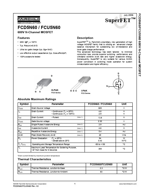
FCD5N60/FCU5N60 600V N-Channel MOSFETSuperFETJuly 2006D-PAKFCD SeriesGSDAbsolute Maximum Ratings ParameterDrain-Source Voltage Drain Current - Continuous (T - Continuous (T Drain Current - PulsedFCD5N60/FCU5N60 600V N-Channel MOSFETPackage Marking and Ordering InformationDevice MarkingDevicePackageReel SizeTape WidthQuantityFCD5N60FCD5N60TM D-PAK 380mm 16mm 2500FCD5N60FCD5N60TF D-PAK 380mm 16mm 2000FCU5N60FCU5N60I-PAK----70Electrical Characteristics T C = 25°C unless otherwise notedSymbolParameterConditionsMinTypMax UnitsOff Characteristics BV DSS Drain-Source Breakdown Voltage V GS = 0V, I D = 250µA, T J = 25°C 600----V V GS = 0V, I D = 250µA, T J = 150°C --650--V ∆BV DSS / ∆T J Breakdown Voltage Temperature CoefficientI D = 250µA, Referenced to 25°C --0.6--V/°C BV DS Drain-Source Avalanche Breakdown VoltageV GS = 0V, I D = 4.6A --700--V I DSS Zero Gate Voltage Drain Current V DS = 600V, V GS = 0V V DS = 480V, T C = 125°C --------110µA µA I GSSF Gate-Body Leakage Current, Forward V GS = 30V, V DS = 0V ----100nA I GSSR Gate-Body Leakage Current, Reverse V GS = -30V, V DS = 0V -----100nA On CharacteristicsV GS(th)Gate Threshold Voltage V DS = V GS , I D = 250µA 3.0-- 5.0V R DS(on)Static Drain-Source On-ResistanceV GS = 10V, I D = 2.3A --0.810.95Ωg FS Forward Transconductance V DS = 40V, I D = 2.3A (Note 4)-- 3.8--S Dynamic CharacteristicsC iss Input Capacitance V DS = 25V, V GS = 0V,f = 1.0MHz--470600pF C oss Output Capacitance--250320pF C rss Reverse Transfer Capacitance --22--pF C oss Output CapacitanceV DS = 480V, V GS = 0V, f = 1.0MHz --12--pF C oss eff.Effective Output Capacitance V DS = 0V to 400V, V GS = 0V --32--pF Switching Characteristicst d(on)Turn-On Delay Time V DD = 300V, I D = 4.6A R G = 25Ω(Note 4, 5)--1230ns t r Turn-On Rise Time --4090ns t d(off)Turn-Off Delay Time --4795ns t f Turn-Off Fall Time --2255ns Q g Total Gate Charge V DS = 480V, I D = 4.6A V GS = 10V(Note 4, 5)--16--nC Q gs Gate-Source Charge -- 2.8--nC Q gd Gate-Drain Charge--7--nCDrain-Source Diode Characteristics and Maximum RatingsI S Maximum Continuous Drain-Source Diode Forward Current ---- 4.6A I SM Maximum Pulsed Drain-Source Diode Forward Current ----13.8A V SD Drain-Source Diode Forward Voltage V GS = 0V, I S = 4.6A---- 1.4V t rr Reverse Recovery Time V GS = 0V, I S = 4.6AdI F /dt =100A/µs (Note 4)--295--ns Q rrReverse Recovery Charge-- 2.7--µCNOTES:1. Repetitive Rating: Pulse width limited by maximum junction temperature2. I AS = 2.3A, V DD = 50V, R G = 25Ω, Starting T J = 25°C3. I SD ≤4.6A, di/dt ≤ 1200A/µs, V DD ≤ BV DSS , Starting T J = 25°C 4. Pulse Test: Pulse width ≤ 300µs, Duty Cycle ≤ 2%5. Essentially Independent of Operating Temperature Typical CharacteristicsResistive Switching Test Circuit & WaveformsUnclamped Inductive Switching Test Circuit & WaveformsFCD5N60/FCU5N60 600V N-Channel MOSFETFCD5N60/FCU5N60 600V N-Channel MOSFETFCD5N60/FCU5N60 600V N-Channel MOSFETTRADEMARKSThe following are registered and unregistered trademarks Fairchild Semiconductor owns or is authorized to use and is not intended to be an exhaustive list of all such trademarks.DISCLAIMERFAIRCHILD SEMICONDUCTOR RESERVES THE RIGHT TO MAKE CHANGES WITHOUT FURTHER NOTICE TO ANY PRODUCTS HEREIN TO IMPROVE RELIABILITY, FUNCTION OR DESIGN. FAIRCHILD DOES NOT ASSUME ANY LIABILITY ARISING OUT OF THE APPLICATION OR USE OF ANY PRODUCT OR CIRCUIT DESCRIBED HEREIN; NEITHER DOES IT CONVEY ANY LICENSE UNDER ITS PATENT RIGHTS, NOR THE RIGHTS OF OTHERS. THESE SPECIFICATIONS DO NOT EXPAND THE TERMS OF FAIRCHILD’S WORLDWIDE TERMS AND CONDITIONS, SPECIFICALLY THE WARRANTY THEREIN, WHICH COVERS THESE PRODUCTS.LIFE SUPPORT POLICYFAIRCHILD’S PRODUCTS ARE NOT AUTHORIZED FOR USE AS CRITICAL COMPONENTS IN LIFE SUPPORT DEVICES OR SYSTEMS WITHOUT THE EXPRESS WRITTEN APPROVAL OF FAIRCHILD SEMICONDUCTOR CORPORATION.As used herein:1. Life support devices or systems are devices or systems which, (a) are intended for surgical implant into the body, or (b) support or sustain life, or (c) whose failure to perform when properly used in accordance with instructions for use provided in the labeling, can be reasonably expected to result in significant injury to the user.2. A critical component is any component of a life support device or system whose failure to perform can be reasonably expected to cause the failure of the life support device or system, or to affect its safety or effectiveness.PRODUCT STATUS DEFINITIONS Definition of TermsACEx™ActiveArray™Bottomless™Build it Now™CoolFET™CROSSVOLT ™DOME™EcoSPARK™E 2CMOS™EnSigna™FACT™FAST ®FASTr™FPS™FRFET™FACT Quiet Series™ GlobalOptoisolator™GTO™HiSeC™I 2C™i-Lo ™ImpliedDisconnect ™IntelliMAX™ISOPLANAR™LittleFET™MICROCOUPLER™MicroFET™MicroPak™MICROWIRE™MSX ™MSXPro ™OCX ™OCXPro ™OPTOLOGIC ®OPTOPLANAR™PACMAN™POP™Power247™PowerEdge™PowerSaver™PowerTrench ®QFET ®QS™QT Optoelectronics™Quiet Series™RapidConfigure ™RapidConnect ™µSerDes ™ScalarPump ™SILENT SWITCHER ®SMART START™SPM™Stealth™SuperFET™SuperSOT™-3SuperSOT™-6SuperSOT™-8SyncFET™TCM™TinyBoost™TinyBuck™TinyPWM™TinyPower™TinyLogic ®TINYOPTO™TruTranslation™UHC™UniFET™UltraFET ®VCX™Wire™Across the board. Around the world.™The Power Franchise ®Programmable Active Droop™Datasheet Identification Product Status DefinitionAdvance InformationFormative or In Design This datasheet contains the design specifications for product development. Specifications may change in any manner without notice.PreliminaryFirst ProductionThis datasheet contains preliminary data, andsupplementary data will be published at a later date.Fairchild Semiconductor reserves the right to make changes at any time without notice in order to improve design.No Identification Needed Full ProductionThis datasheet contains final specifications. Fairchild Semiconductor reserves the right to make changes at any time without notice in order to improve design. Obsolete Not In ProductionThis datasheet contains specifications on a product that has been discontinued by Fairchild semiconductor.The datasheet is printed for reference information only.Rev. I20。

5n60场效应管参数场效应管(FieldEffectTransistor,FET)是一类半导体器件,它具有低功率消耗和高频率特性。
5n60场效应管是一种具有较高性能的场效应管,它可以提供高压和高电流,可以用于电路设计的高效率和高可靠性的应用。
5n60场效应管的参数包括器件的功耗、特性参数和输入输出特性。
5n60场效应管的功耗参数是指器件在不同工作状态下的功率消耗。
常用的功耗参数有功耗系数,关於功耗系数可以从两个方面来描述,一是指器件在饱和状态下功耗,即IC(集成电路);另一种是指在不饱和状态下功耗,即IGSS。
功耗系数越低表明器件功耗越小,也表示器件整体更加经济高效。
5n60场效应管的特性参数指的是器件的其他性能参数,包括器件的静态特性(如截止电压Vt,和漏源电压Vds),和动态特性(如开关时间toff和上升/下降时间tr/tf)。
其中,截止电压Vt是指在放大电流时,场效应管的源极和漏极之前的阈值电压;漏源电压Vds 是指场效应管漏极对场效应管源极的绝对值电压;开关时间toff是指场效应管从关断时到开启时所需要的时间;上升/下降时间tr/tf 则是指场效应管上升或下降到最终转换阈值电压Vt所需要的时间。
5n60场效应管的输入输出特性主要是指器件的输入电压波形和输出电流波形。
一般情况下,输入电压和输出电流都是逐渐上升或下降的,但也可能出现瞬时突变的情况,这取决于器件的工作状态。
器件的输入电压有可能出现多次上升或下降,而输出电流只有一次上升和一次下降,这两个特性都是由器件的工作状态决定的。
5n60场效应管参数的重要性在于它可以根据电路的不同性能要求来配置器件,使用户可以计算出最佳的工作状态,以产生最大的输出和最佳的功效。
此外,正确的参数也可以节约电路的功耗,减少噪声,提高电路的稳定性,确保设计电路的功能和可靠性。
因此,了解场效应管参数对电路设计至关重要,特别是对于5n60场效应管来说,更需要了解器件的功率消耗、特性参数和输入输出特性,以确保电路性能和可靠性。
DDecember 2008 SuperFETFCD5N60 / FCU5N60 600V N-Channel MOSFET rchild’s proprietary, new generation of high voltage MOSFET family that is utilizing an advanced charge balance mechanism for outstanding low on-resistance and This advanced technology has been tailored to minimizeD-PAKFCD Series G SFCD5N60 / FCU5N60 600V N-Channel MOSFETPackage Marking and Ordering InformationDevice MarkingDevicePackageReel SizeTape WidthQuantityFCD5N60FCD5N60TM D-PAK 380mm 16mm 2500FCD5N60FCD5N60TF D-PAK 380mm 16mm 2000FCU5N60FCU5N60I-PAK----70Electrical Characteristics T C= 25°C unless otherwise notedSymbolParameterConditionsMinTypMax UnitsOff Characteristics BV DSS Drain-Source Breakdown Voltage V GS = 0V, I D = 250μA, T J = 25°C 600----V V GS = 0V, I D = 250μA, T J = 150°C --650--V ΔBV DSS / ΔT J Breakdown Voltage Temperature CoefficientI D = 250μA, Referenced to 25°C --0.6--V/°C BV DS Drain-Source Avalanche Breakdown VoltageV GS = 0V, I D = 4.6A --700--V I DSS Zero Gate Voltage Drain Current V DS = 600V, V GS = 0V V DS = 480V, T C = 125°C --------110μA μA I GSSF Gate-Body Leakage Current, Forward V GS = 30V, V DS = 0V ----100nA I GSSR Gate-Body Leakage Current, Reverse V GS = -30V, V DS = 0V -----100nA On CharacteristicsV GS(th)Gate Threshold Voltage V DS = V GS , I D = 250μA 3.0-- 5.0V R DS(on)Static Drain-Source On-ResistanceV GS = 10V, I D = 2.3A --0.810.95Ωg FS Forward Transconductance V DS = 40V, I D = 2.3A (Note 4)-- 3.8--S Dynamic CharacteristicsC iss Input Capacitance V DS = 25V, V GS = 0V,f = 1.0MHz--470600pF C oss Output Capacitance--250320pF C rss Reverse Transfer Capacitance --22--pF C oss Output CapacitanceV DS = 480V, V GS = 0V, f = 1.0MHz --12--pF C oss eff.Effective Output Capacitance V DS = 0V to 400V, V GS = 0V --32--pF Switching Characteristicst d(on)Turn-On Delay Time V DD = 300V, I D = 4.6A R G = 25Ω(Note 4, 5)--1230ns t r Turn-On Rise Time --4090ns t d(off)Turn-Off Delay Time --4795ns t f Turn-Off Fall Time --2255ns Q g Total Gate Charge V DS = 480V, I D = 4.6A V GS = 10V(Note 4, 5)--16--nC Q gs Gate-Source Charge -- 2.8--nC Q gd Gate-Drain Charge--7--nCDrain-Source Diode Characteristics and Maximum RatingsI S Maximum Continuous Drain-Source Diode Forward Current ---- 4.6A I SM Maximum Pulsed Drain-Source Diode Forward Current ----13.8A V SD Drain-Source Diode Forward Voltage V GS = 0V, I S = 4.6A---- 1.4V t rr Reverse Recovery Time V GS = 0V, I S = 4.6AdI F /dt =100A/μs (Note 4)--295--ns Q rrReverse Recovery Charge-- 2.7--μCNOTES:1. Repetitive Rating: Pulse width limited by maximum junction temperature2. I AS = 2.3A, V DD = 50V, R G = 25Ω, Starting T J = 25°C3. I SD ≤4.6A, di/dt ≤ 200A/μs, V DD ≤ BV DSS , Starting T J = 25°C 4. Pulse Test: Pulse width ≤ 300μs, Duty Cycle ≤ 2%5. Essentially Independent of Operating Temperature Typical CharacteristicsUnclamped Inductive Switching Test Circuit & WaveformsFCD5N60 / FCU5N60 600V N-Channel MOSFETFCD5N60 / FCU5N60 600V N-Channel MOSFET* EZSWITCH™ and FlashWriter ® are trademarks of System General Corporation, used under license by Fairchild Semiconductor.DISCLAIMERFAIRCHILD SEMICONDUCTOR RESERVES THE RIGHT TO MAKE CHANGES WITHOUT FURTHER NOTICE TO ANY PRODUCTS HEREIN TO IMPROVE RELIABILITY, FUNCTION, OR DESIGN. FAIRCHILD DOES NOT ASSUME ANY LIABILITY ARISING OUT OF THE APPLICATION OR USE OF ANY PRODUCT OR CIRCUIT DESCRIBED HEREIN; NEITHER DOES IT CONVEY ANY LICENSE UNDER ITS PATENT RIGHTS, NOR THE RIGHTS OF OTHERS.THESE SPECIFICATIONS DO NOT EXPAND THE TERMS OF FAIRCHILD’S WORLDWIDE TERMS AND CONDITIONS, SPECIFICALLY THE WARRANTY THEREIN, WHICH COVERS THESE PRODUCTS.LIFE SUPPORT POLICYFAIRCHILD’S PRODUCTS ARE NOT AUTHORIZED FOR USE AS CRITICAL COMPONENTS IN LIFE SUPPORT DEVICES OR SYSTEMS WITHOUT THE EXPRESS WRITTEN APPROVAL OF FAIRCHILD SEMICONDUCTOR CORPORATION.As used herein:1. Life support devices or systems are devices or systems which, (a) are intended for surgical implant into the body or (b) support or sustain life,and (c) whose failure to perform when properly used in accordance with instructions for use provided in the labeling, can be reasonably expected to result in a significant injury of the user. 2. A critical component in any component of a life support, device, orsystem whose failure to perform can be reasonably expected to cause the failure of the life support device or system, or to affect its safety or effectiveness.PRODUCT STATUS DEFINITIONS Definition of TermsBuild it Now™CorePLUS™CorePOWER™CROSSVOLT ™CTL™Current Transfer Logic™EcoSPARK ®EfficentMax™EZSWITCH™ *™Fairchild ®Fairchild Semiconductor ®FACT Quiet Series™FACT ®FAST ®FastvCore™FlashWriter ® *FPS™F-PFS™FRFET ®Global Power Resource SM Green FPS™Green FPS™ e-Series™GTO™IntelliMAX™ISOPLANAR™MegaBuck™MICROCOUPLER™MicroFET™MicroPak™MillerDrive™MotionMax™Motion-SPM™OPTOLOGIC ®OPTOPLANAR ®®PDP SPM™Power-SPM™PowerTrench ®PowerXS™Programmable Active Droop™QFET ®QS™Quiet Series™RapidConfigure™™Saving our world, 1mW /W /kW at a time™SmartMax™SMART START™SPM ®STEALTH™SuperFET™SuperSOT™-3SuperSOT™-6SuperSOT™-8SupreMOS™SyncFET™®The Power Franchise ®TinyBoost™TinyBuck™TinyLogic ®TINYOPTO™TinyPower™TinyPWM™TinyWire™μSerDes™UHC ®Ultra FRFET™UniFET™VCX™VisualMax™XS™®Datasheet Identification Product Status DefinitionAdvance InformationFormative / In DesignDatasheet contains the design specifications for product development. Specifications may change in any manner without notice.ANTI-COUNTERFEITING POLICYFairchild Semiconductor Corporation’s Anti-Counterfeiting Policy. Farichild’s Anti-Counterfeiting Policy is also stated on our external website,, under Sales Support .Counterfeiting of semiconductor parts is a growing problem in the industry. All manufactures of semiconductor products are experiencing counterfeiting of their parts. Customers who inadvertently purchase counterfeit parts experience many problems such as loss of brand reputation, substandard performance, failed application, and increased cost of production and manufacturing delays. Fairchild is taking strong measures to protect ourselves and our customers from the proliferation of counterfeit parts. Farichild strongly encourages customers to purchase Farichild parts either directly from Fairchild or from Authorized Fairchild Distributors who are listed by country on our web page cited above. Products customers buy either from fairchild directly or from Authorized Fairchild Distributors are genuine parts, have full traceability, meet Fairchild’s quality standards for handing and storage and provide access to Farichild’s full range of up-to-date technical and product information. Fairchild and our Authorized Distributors will stand behind all warranties and will appropriately address and warranty issues that may arise. Fairchild will not provide any warranty coverage or other assistance for parts bought from Unauthorized Sources. Farichild is committed to combat this global problem and encourage our customers to do their part in stopping this practice by buying direct or from authorized distributors.FCD5N60 / FCU5N60 600V N-Channel MOSFET。
STD5N60DM2DPAKFeatures•Fast-recovery body diode•Extremely low gate charge and input capacitance•Low on-resistance•100% avalanche tested•Extremely high dv/dt ruggedness•Zener-protectedApplications•Switching applicationsDescriptionThis high-voltage N-channel Power MOSFET is part of the MDmesh™ DM2 fast recovery diode series. It offers very low recovery charge (Q rr) and time (t rr) combined with low R DS(on), rendering it suitable for the most demanding high-efficiency converters and ideal for bridge topologies and ZVS phase-shift converters.N-channel 600 V, 1.38 Ω typ., 3.5 A MDmesh™ DM2Power MOSFET in a DPAK packageSTD5N60DM2DatasheetSTD5N60DM2Electrical ratings 1Electrical ratingsTable 1. Absolute maximum ratings1.Pulse width is limited by safe operating area.2.I SD ≤3.5 A, di/dt=400 A/μs; V DS peak < V(BR)DSS, V DD = 480 V.3.V DS ≤ 480 V.Table 2. Thermal data1.When mounted on a 1-inch² FR-4, 2 Oz copper board.Table 3. Avalanche characteristics1.Pulse width limited by T jmax.2.Starting T j = 25 °C, I D = I AR, V DD = 50 V.STD5N60DM2Electrical characteristics 2Electrical characteristics(T case = 25 °C unless otherwise specified).Table 4. Static1.Defined by design, not subject to production test.Table 5. Dynamic1.C oss eq. is defined as a constant equivalent capacitance giving the same charging time as C oss when V DS increases from 0to 80% V DSS.Table 6. Switching timesSTD5N60DM2Electrical characteristicsTable 7. Source-drain diode1.Pulse width is limited by safe operating area.2.Pulse test: pulse duration = 300 µs, duty cycle 1.5%.STD5N60DM2Electrical characteristics (curves) 2.1Electrical characteristics (curves)STD5N60DM2 Electrical characteristics (curves)STD5N60DM2 Electrical characteristics (curves)STD5N60DM2Test circuits 3Test circuitsSTD5N60DM2Package information 4Package informationIn order to meet environmental requirements, ST offers these devices in different grades of ECOPACK®packages, depending on their level of environmental compliance. ECOPACK® specifications, grade definitionsand product status are available at: . ECOPACK® is an ST trademark.4.1DPAK (TO-252) type A package informationFigure 19. DPAK (TO-252) type A package outline0068772_A_25Table 8. DPAK (TO-252) type A mechanical data4.2DPAK (TO-252) type E package informationFigure 20. DPAK (TO-252) type E package outline0068772_type-E_rev.25Table 9. DPAK (TO-252) type E mechanical dataFigure 21. DPAK (TO-252) type E recommended footprint (dimensions are in mm)FP_0068772_254.3DPAK (TO-252) packing informationFigure 22. DPAK (TO-252) tape outlineP0K 0U ser direction of feed10 pitches cumulativetolerance on tape +/- 0.2 mmU ser direction of feedRBending radiusB 1including draft andradii concentric around B0AM08852v1Figure 23. DPAK (TO-252) reel outlineAM06038v1 Table 10. DPAK (TO-252) tape and reel mechanical dataRevision historyTable 11. Document revision historyContentsContents1Electrical ratings (2)2Electrical characteristics (3)2.1Electrical characteristics (curves) (5)3Test circuits (8)4Package information (9)4.1DPAK (TO-252) type A package information (9)4.2DPAK (TO-252) type E package information (11)4.3DPAK (TO-252) packing information (13)Revision history (16)IMPORTANT NOTICE – PLEASE READ CAREFULLYSTMicroelectronics NV and its subsidiaries (“ST”) reserve the right to make changes, corrections, enhancements, modifications, and improvements to ST products and/or to this document at any time without notice. Purchasers should obtain the latest relevant information on ST products before placing orders. ST products are sold pursuant to ST’s terms and conditions of sale in place at the time of order acknowledgement.Purchasers are solely responsible for the choice, selection, and use of ST products and ST assumes no liability for application assistance or the design of Purchasers’ products.No license, express or implied, to any intellectual property right is granted by ST herein.Resale of ST products with provisions different from the information set forth herein shall void any warranty granted by ST for such product.ST and the ST logo are trademarks of ST. All other product or service names are the property of their respective owners.Information in this document supersedes and replaces information previously supplied in any prior versions of this document.© 2018 STMicroelectronics – All rights reservedSTD5N60DM2。
fqp5n60c的应用原理1. 简介fqp5n60c是一款具有广泛应用的N-沟道MOSFET(金属氧化物场效应晶体管),广泛用于电源管理、电机控制和电子开关等领域。
本文将介绍fqp5n60c的基本原理及其应用。
2. fqp5n60c的基本原理fqp5n60c采用N-沟道结构,是一种增强型MOSFET。
它由沟道、栅极、漏极和源极四个主要部分组成。
•沟道:沟道是一个N型掺杂层,用于导电。
电流在这个沟道中流动。
•栅极:栅极是通过输入控制信号来改变沟道电阻的部分。
栅极电压的变化会影响沟道的导电能力。
•漏极和源极:漏极和源极是电流的进出口,电流通过漏极从源极流出。
fqp5n60c的工作原理是通过调节栅极电压来控制沟道的导电能力。
当栅极电压高于一定阈值时,沟道会打开,导通电流。
当栅极电压低于阈值时,沟道关闭,截断电流。
通过控制栅极电压可以实现对电流的控制和开关。
3. fqp5n60c的应用fqp5n60c由于其优异的特性,在各种电子领域中得到了广泛应用。
以下是fqp5n60c的几种常见应用:3.1 电源管理fqp5n60c可以用作电源开关,通过控制其导电能力来实现对电源的开关和调节。
它在电源管理中具有低导通电阻、高输入电容和低开关损耗等特点,适用于交流/直流转换器、开关电源和逆变器等电源管理系统。
3.2 电机控制由于fqp5n60c具有较低的导通电阻和较高的开关速度,可以在电机控制中广泛应用。
它可以用作驱动MOSFET,用于电机启动和调速控制。
fqp5n60c的低导通电阻可以减少能量损耗,提高电机的效率。
3.3 电子开关fqp5n60c作为一个高效可靠的电子开关,可以在电子电路中用于开关操作。
它可以用于开关电源、LED驱动器、电路保护和信号放大器等应用。
其快速开关速度和低开关损耗使其非常适合高频应用。
3.4 其他应用除了上述应用,fqp5n60c还可以在其他电子系统中扮演关键角色。
例如,在电流限制器、电压稳定器和逆变器中,它的优异特性使其成为理想的选择。