AXA003A0XZ;AXA003A0X4Z;AXA003A0X;AXA003A0X4;中文规格书,Datasheet资料
- 格式:pdf
- 大小:472.42 KB
- 文档页数:11

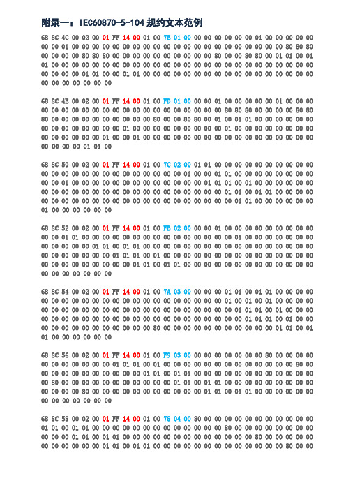
68 04 07 00 00 00 /* U格式启动帧 */68 04 0B 00 00 00 /* 响应帧 */68 0E 00 00 02 00 64 01 06 00 01 00 00 00 0014/* I格式总召帧 */68 0E 44 00 02 00 64 01 07 00 01 00 00 00 0014/* 总召激活帧 *//* 总召遥信帧 */68 8C 46 00 02 00 01 FF 14 00 01 00 01 00 00 00 00 01 01 00 01 01 00 00 00 00 00 00 00 00 00 00 00 00 00 00 00 00 00 00 00 00 00 00 00 00 00 00 00 00 00 00 00 00 00 00 00 00 00 00 00 00 00 00 00 00 00 00 00 00 00 00 00 00 00 00 00 00 00 00 00 00 00 00 00 00 00 00 00 00 00 00 00 00 00 00 00 80 00 01 01 00 01 01 00 00 00 00 00 00 00 00 00 00 00 00 00 00 00 00 00 00 00 00 00 00 00 00 00 00 00 00 00 01 00 00 01 00 00 00 00 0068 8C 48 00 02 00 01 FF 14 00 01 00 80 00 00 00 00 00 00 00 00 00 00 00 00 00 00 00 00 00 00 00 00 00 00 00 00 00 00 00 00 00 00 00 00 00 00 00 80 00 01 00 00 0000 00 00 00 00 00 00 00 00 00 00 00 00 00 00 00 00 00 00 00 00 00 00 00 00 00 0001 00 00 00 00 01 00 00 00 00 01 01 01 01 00 00 00 00 00 00 00 00 00 00 00 00 00 00 00 00 00 01 01 00 01 00 00 00 00 00 00 00 00 01 00 01 00 00 00 00 00 00 00 00 00 00 00 00 00 00 0068 8C 4A 00 02 00 01 FF 14 00 01 00 FF 00 00 00 00 00 00 00 00 00 00 00 00 00 00 01 01 00 00 00 00 01 00 00 00 00 00 00 00 01 00 01 00 00 01 01 00 00 01 00 00 00 00 00 00 00 00 00 00 00 00 00 00 00 00 00 00 00 01 00 00 00 00 00 00 00 00 00 00 00 00 01 01 00 01 01 00 00 00 00 00 00 00 00 00 00 00 00 00 00 00 00 00 00 00 00 00 00 00 00 00 00 00 00 00 00 01 01 00 00 01 01 00 00 00 00 00 00 00 00 00 00 00 00 00 00 00 00 00 0068 8C 4C 00 02 00 01 FF 14 00 01 00 7E 01 00 00 00 00 00 00 00 01 00 00 00 00 00 00 00 01 00 00 00 00 00 00 00 00 00 00 00 00 00 00 00 00 00 00 00 00 00 80 80 8000 00 00 00 80 80 80 00 00 00 00 00 00 00 00 00 00 80 00 00 80 80 00 01 01 00 0101 00 00 00 00 00 00 00 00 00 00 00 00 00 00 00 00 00 00 00 00 00 00 00 00 00 00 00 00 00 00 01 01 00 00 01 01 00 00 00 00 00 00 00 00 00 00 00 00 00 00 00 00 00 00 00 00 00 00 00 0068 8C 4E 00 02 00 01 FF 14 00 01 00 FD 01 00 00 00 01 00 00 00 00 00 01 00 00 00 00 00 00 00 00 00 00 00 00 00 00 00 00 00 00 00 00 00 80 80 80 00 00 00 00 80 80 80 00 00 00 00 00 00 00 00 00 00 80 00 00 80 80 00 01 00 01 01 00 00 00 00 00 00 00 00 00 00 00 00 00 00 01 00 00 00 00 00 00 00 00 00 01 00 00 00 00 00 00 00 00 00 00 00 00 00 00 01 00 00 01 00 00 00 00 00 00 00 00 00 00 00 00 00 00 00 00 00 00 00 00 00 01 01 0068 8C 50 00 02 00 01 FF 1400 01 00 7C 02 00 01 01 00 00 00 00 00 00 00 00 00 00 00 00 00 00 00 00 00 00 00 00 00 00 00 00 01 00 00 01 01 00 00 00 00 00 00 00 00 00 00 01 00 00 00 00 00 00 00 00 00 00 00 00 00 01 01 01 00 01 00 00 00 00 00 00 00 00 00 00 00 00 00 00 00 00 00 00 00 00 00 00 00 00 01 01 00 01 01 00 00 00 0000 00 00 00 00 00 00 00 00 00 00 00 00 00 00 00 00 00 00 01 01 00 00 00 00 00 0001 00 00 00 00 00 0068 8C 52 00 02 00 01 FF 1400 01 00 FB 02 00 00 00 01 00 00 00 00 00 00 00 00 00 00 00 01 01 00 00 00 00 00 00 00 00 00 00 00 00 00 00 00 01 00 00 00 00 00 00 00 00 00 00 00 00 01 01 00 01 01 00 00 00 00 00 00 00 00 00 00 00 00 00 00 00 00 00 00 00 00 00 00 00 00 01 01 01 00 01 00 00 00 00 00 00 00 00 00 00 00 00 00 00 00 00 00 00 00 00 00 00 00 00 01 01 00 01 01 00 00 00 00 00 00 00 00 00 00 00 00 00 00 00 00 00 00 00 0068 8C 54 00 02 00 01 FF 14 00 01 00 7A 03 00 00 00 00 01 01 00 01 01 00 00 00 00 00 00 00 00 00 00 00 00 00 00 00 00 00 00 00 00 00 00 01 00 01 00 01 00 00 00 00 00 00 00 00 00 00 00 00 00 00 00 00 00 00 00 00 00 00 00 01 01 01 00 01 00 00 00 00 00 00 00 00 00 00 00 00 00 00 00 00 00 00 00 00 00 00 00 01 01 01 00 01 00 0000 00 00 00 00 00 00 00 00 00 00 80 00 00 00 00 00 00 00 00 00 00 00 01 01 00 0101 00 00 00 00 00 0068 8C 56 00 02 00 01 FF 1400 01 00 F9 03 00 00 00 00 00 00 00 00 80 00 00 00 00 00 00 00 00 00 00 00 01 01 01 00 01 00 00 00 00 00 00 00 00 00 00 00 00 00 80 00 00 00 00 00 00 00 00 00 00 00 01 01 00 01 01 00 00 00 00 00 00 00 00 00 00 00 00 00 80 00 00 00 00 00 00 00 00 00 00 00 01 01 00 01 01 00 00 00 00 00 00 00 00 00 00 00 00 00 80 00 00 00 00 00 00 00 00 00 00 00 01 01 00 01 01 00 00 00 00 00 00 00 00 00 00 00 00 0068 8C 58 00 02 00 01 FF 1400 01 00 78 04 00 80 00 00 00 00 00 00 00 00 00 00 00 01 01 00 01 01 00 00 00 00 00 00 00 00 00 00 00 00 00 80 00 00 00 00 00 00 00 00 00 00 00 01 01 00 01 01 00 00 00 00 00 00 00 00 00 00 00 00 00 80 00 00 00 00 00 00 00 00 00 00 00 01 01 00 01 01 00 00 00 00 00 00 00 00 00 00 00 00 00 80 00 0000 00 00 00 00 00 00 00 00 01 01 01 00 01 00 00 00 00 00 00 00 00 00 00 00 00 00 80 00 00 00 00 00 0068 2C 5A 00 02 00 01 9F 14 00 01 00 F7 04 00 00 00 00 00 01 00 00 00 00 00 00 00 00 00 00 00 00 00 00 00 00 00 00 00 00 00 00 00 00 00 00/* 总召遥测帧 */68 8D 5C 00 02 00 15 C0 14 00 01 00 01 40 00 0B 04 0D 04 09 04 69 00 79 00 67 00 40 FD EC FF CE FF AA 06 0C 04 09 04 09 04 27 02 21 02 3D 02 4B F8 F0 FE B6 FF AA 06 0B 04 0B 04 09 04 00 00 00 00 00 00 00 00 00 00 00 00 0B 04 0C 04 09 04 00 00 02 07 01 07 00 07 1F 06 1A 06 77 04 4B 04 EA 04 12 05 00 00 00 00 00 00 00 00 00 00 73 05 75 05 58 05 5A 05 37 01 12 01 1B 01 00 00 00 00 00 00 E5 03 DF 03 F0 03 10 00 C4 06 C3 06 BC 0668 8D 5E 00 02 00 15 C0 14 00 01 00 41 40 00 E9 03 D0 03 F2 03 22 00 BD 06 BE 06 BD 06 0A 04 0C 04 0A 04 54 02 4B 02 52 02 3E 07 0E 01 7C 00 E6 03 DF 03 EF 03 D6 03 D6 03 DB 03 84 07 C3 01 A2 00 0B 04 0B 04 09 04 9A 02 96 02 99 02 67 07 37 01 7E 00 E8 03 D0 03 F3 03 4D 04 4B 04 46 04 A6 07 01 02 9A 00 00 00 00 00 00 00 00 00 00 00 00 00 00 00 00 00 00 00 00 00 00 00 00 00 00 00 00 00 00 00 00 00 8D 01 94 01 98 01 96 07 BC 0068 8D 60 00 02 00 15 C0 14 00 01 00 81 40 00 3B 00 00 00 00 00 00 00 00 00 00 00 00 00 00 00 00 00 00 00 00 00 00 00 00 00 00 00 00 00 00 00 00 00 00 00 00 00 57 03 54 03 57 03 4C 07 79 01 A7 00 D2 01 CF 01 CE 01 A0 07 DB 00 43 00 E5 01 EE 01 ED 01 BB 07 E7 00 3F 00 32 02 2A 02 26 02 EA 07 09 01 22 00 38 02 2E 02 29 02 E8 07 0C 01 27 00 F5 02 F1 02 FB 02 BD 07 6A 01 5F 00 3B 00 44 00 39 00 74 FC F4 FF 19 00 0A 00 08 00 0B 0068 8B 62 00 02 00 15 BF 14 00 01 00 C1 40 00 FF 07 04 00 FE FF 00 00 00 00 00 00 00 00 00 00 00 00 39 02 38 02 3B 02 40 07 FA 00 75 00 00 00 00 00 00 00 00 00 00 00 00 00 8A 06 8B 06 98 06 92 07 04 03 FF 00 00 00 00 00 00 00 00 00 00 00 00 00 00 00 00 00 00 00 00 00 00 00 00 00 17 00 16 00 17 00 FF 07 0A 00 00 00 2A 00 2A 00 2E 00 FF 07 17 00 01 00 21 04 1E 04 23 04 6F 07 DD 01 BB 00 16 00 16 00 16 00 75 06 08 00 05 0068 0E 64 00 02 00 64 01 0A 00 01 00 00 00 0014/* 总召激活终止帧 *//* 对时报文 */68 14 08 00 04 00 67 01 0600 01 00 00 00 0020 00 1E 08 18 0A 0668 14 0A 00 04 00 67 0107 00 01 00 00 00 0020 00 1E 08 18 0A 06|> |-------------| | | |-----| |-----| |---------| |--------------------------| 长度帧计数 | 个数原因主站地址信息地址 CP56Time2a时标类型毫秒L-毫秒H-分-时-日-月-年68 04 43 00 00 00 /* 链路测试报文 */68 04 83 00 00 00 /* 响应帧 *//* 变化遥测帧 */68 AA 64 00 02 00 15 20 03 00 01 00 01 40 00 05 04 02 40 00 05 04 03 40 00 18 04 07 40 00 24 FD 0F 40 00 26 02 3E 40 00 C4 06 3F 40 00 BD 06 4C 40 00 51 02 50 40 00 81 00 55 40 00 DC 03 66 40 00 59 04 81 40 00 42 00 95 40 00 56 03 97 40 00 53 07 9A 40 00 C9 01 9B 40 00 C8 01 9C 40 00 C6 01 9E 40 00 D3 00 A2 40 00 ED 01 A7 40 00 2E 02 A8 40 00 2C 02 AA 40 00 11 01 AC 40 00 37 02 AD 40 00 2C 02 B8 40 00 35 00 B9 40 00 47 00 BB 40 00 71 FE C7 40 00 B9 FD CA 40 00 3E 02 CB 40 00 3E 02 CC 40 00 41 02 D6 40 00 86 06/* 变位遥信帧 */68 16 0E 00 0A 00 01 03 0300 01 00 01 00 00 01 02 00 00 01 03 00 00 01|> |-------------| | | |-----| |-----| |---------| | |---------| | |--------| | 长度帧计数 | 个数原因主站地址遥信地址值遥信地址值遥信地址值类型/* SOE事件帧 */68 15 10 00 0C 00 1E 01 0300 01 00 01 00 00 01 01 62 3A 08 18 0A 06|> |-------------| | | |-----| |-----| |---------| | |-------------------------| 长度帧计数 | 个数原因主站地址遥信地址值 CP56Time2a时标类型毫秒L-毫秒H-分-时-日-月-年68 0E 12 00 0E 00 2E 01 0600 01 00 01 60 0081/* 双点遥控分选择 */68 0E 12 00 0E 00 2E 01 07 00 01 00 01 60 0081 /* 遥控返校 */|> |-------------| | | |-----| |-----| |---------| |长度帧计数 | 个数原因主站地址信息地址双命令类型68 0E 12 00 0E 00 2E 01 0600 01 00 01 60 0001/* 双点遥控分执行 */68 0E 12 00 0E 00 2E 01 07 00 01 00 01 60 0001 /* 遥控返校 */68 0E 12 00 0E 00 2D 01 0600 01 00 01 60 0080/* 单点遥控分选择 */68 0E 12 00 0E 00 2D 01 07 00 01 00 01 60 0080 /* 遥控返校 */68 0E 14 00 10 00 2D 01 06 00 01 00 01 60 0000/* 单点遥控分执行 */68 0E 14 00 10 00 2D 01 07 00 01 00 01 60 0000 /* 遥控返校 */|> |-------------| | | |-----| |-----| |---------| |长度帧计数 | 个数原因主站地址信息地址单命令类型68 0E 14 00 10 00 2D 01 08 00 01 00 01 60 0080/* 单点遥控分撤销 */68 0E 14 00 10 00 2D 01 09 00 01 00 01 60 0080 /* 遥控返校 */68 04 01 00 12 00 /* S格式计数帧 */|> |-----| |------|长度 S格式帧接收序号电力104规约典型报文附带一份报文解析文件,1.U格式的STARTDT生效报文(主站→子站)68 04 07 00 00 002.U格式的STARTDT确认报文(子站→主站)68 04 0B 00 00 003.总召唤启动报文(主站→子站)68 0E 00 00 00 00 64 01 06 00 00 00 00 00 00 144.总召唤确认报文(子站→主站)68 0E 0E 00 02 00 64 01 07 00 00 00 00 00 00 145.总召唤结束报文(子站→主站)68 0E 18 00 02 00 64 01 0A 00 00 00 00 00 00 146.全遥信报文68 2D 14 00 02 00 01 A0 14 00 00 00 81 00 00 00 00 00 00 00 00 00 00 00 00 00 00 00 00 00 00 00 00 00 00 00 00 00 00 00 00 00 00 00 00 00 007.全遥测报文68 2D 16 00 02 00 15 90 14 00 00 00 01 07 00 00 00 00 00 00 00 00 00 00 00 00 00 00 00 00 00 00 00 00 00 00 00 00 00 00 00 00 00 00 00 00 008.遥控选择报文68 0E 00 00 00 00 2E 01 06 00 00 00 21 0B 00 859.遥控返校报文68 0E 00 00 00 00 2E 01 07 00 00 00 21 0B 00 8510.遥控执行报文68 0E 00 00 00 00 2E 01 06 00 00 00 21 0B 00 0511.遥控执行确认报文68 0E 00 00 00 00 2E 01 07 00 00 00 21 0B 00 0512.遥控撤销报文68 0E 00 00 00 00 2E 01 08 00 00 00 21 0B 00 0513.遥控撤销确认报文68 0E 00 00 00 00 2E 01 09 00 00 00 21 0B 00 0514.COS报文68 0E 00 00 00 00 01 01 03 00 00 00 01 00 00 0115.SOE报文68 11 00 00 00 00 02 01 03 00 00 00 01 00 00 01 21 01 20。

1。
微型计算机由那些基本功能部件组成?1).微处理器,2)主存储器,3)系统总线,4)辅助存储器,5)输入/输出(I/O)接口和输入/输出设备2.什么是总线?在计算机中,连接CPU与各个功能部件之间的一组公共线路,称为总线,在计算机中一般有三组功能不同的总线,传输地址信息的称为地址总线,传输数据信息的称为数据总线,传输控制信息的称为控制总线。
(只要答出总线定义,即可)3.简述微型计算机主要特点。
电子计算机是一种能自动,高速,精确地完成各式各样的数据存储,数值计算,逻辑推理,过程控制和数据处理功能的电子机器.计算机的主要特点有四个方面,即:高速性,准确性,逻辑性,通用性。
(只要意思相近即可得分)4.BCD码运算修正规则是什么?BCD码运算修正规则:(1)凡是对应位运算结果为冗余码时,加(减)6修正。
(2)如该位和数有向高位进(借)位时,也在该位加(减)6修正。
(3)如低位修正结果使高位大于9时,高位进行加(减)6修正。
(只要意思相近即可)5.简述微处理器的基本功能。
CPU是组成微机系统的核心部件,其功能如下:(1)算术和逻辑运算,执行数据处理.(2)暂存数据。
(3)实现程序控制,即可取指令,对指令寄存,译码分析并执行指令所规定的操作,还能提供整个系统所需的定时和控制信号。
6.什么是机器数?什么是机器数的真值?数在机器内的表示形式为机器数。
而机器数对应的数值称为机器数的真值8个总线周期8. 8086CPU内部由哪两部分组成?各完成什么工作?在8086内部由BIU和EU两大部分组成,BIU主要负责和总线打交道,用于CPU与存储器和I/O接口之间进行数据交换;EU主要是将从指令队列中取得的指令加以执行。
9. 简述8086内部EU和BIU两大功能单元各自的功能和这样组织的意义。
在8086内部,按功能划分可以分为BIU和EU两大部分,BIU主要负责总线接口,与存储器和I/O接口进行数据传递;而EU则是执行部件,主要是执行指令;这两部分分开可以在执行指令的同时,从存储器中将将要执行的指令取到指令队列,使两部分并行工作,提高CPU的速度.(只要意思为提高CPU的效率即可)10。
中国移动通信企业标准QB-╳╳-╳╳╳-╳╳╳╳中国移动V o L T E试点测试规范(网络功能及基本业务分册)C h i n a M o b i l e V o L T E T r i a l T e s tS p e c i f i c a t i o n--N e t w o r k f u n c t i o na n d B a s i c S e r v i c e版本号:1.3.1╳╳╳╳-╳╳-╳╳发布╳╳╳╳-╳╳-╳╳实施目录前言 ............................................................................................................................................ I II1.范围 (1)2.规范性引用文件 (1)3.术语、定义和缩略语 (1)4.测试环境和方法 (3)4.1 测试设备 (3)4.2 测试工具 (4)4.3 测试方法 (4)4.4 测试组网图 (4)4.5 测试配置 (4)5.测试用例 (5)5.1 VoLTE基础功能测试 (5)5.1.1 VoLTE基础功能测试 (5)5.2 端到端业务流程 (134)5.2.1 VoLTE基本呼叫及切换流程 (134)5.2.2 补充业务 (300)5.3 其它业务 (414)5.3.1 IP短消息 (414)5.3.2 紧急呼叫 (447)5.4 业务质量及性能指标 (450)5.4.1 业务指标测试 (450)5.4.2 终端测试 (454)6 编制历史 (468)前言本测试规范对中国移动通信集团公司VoLTE业务涉及的测试相关内容进行规定,是VoLTE测试实施的依据。
本测试规范共分四册,分别为网络功能及基本业务分册、增值业务分册、开通及计费分册和无线性能分册。
中国移动VoLTE外场测试系列规范用于VoLTE外场试验城市端到端环境的测试,指导测试无线网络、核心网络及终端等方面的功能与性能。

光缆巡检编码规则2013年4月
为了简化编码规则,对于各种设施可采用统一编码规则的方式进行,编码规则如下:
说明:
1.名称符号: 采用该线路大写首字母进行拼接,两地名之间用“-”
相连;
2.连接符:固定为“/-”;
3.标识符:为各种设施的标识符,如下表所示:
4.序号:根据实际情况,在标识所描述的范围内按一定规则从001
开始编号;
5.扩充后缀:对于扩充新增的电杆和小区内道路电杆的分支杆等情
况,需要加入扩充字符,从小写字母‘a’开始;
示例:广州到上海光缆中依次如下,其中第4个电杆是后期新建的:
1 光缆配线架2光缆终端盒3 电杆4 电杆5 电杆6管道闸7人手井8管道里程标桩…
则编码如下:
XA-YA/GB002 XA-YA/P003 XA-YA/P003a XA-YA/P004 XA-YA/GDZ005 XA-YA/#006 XA-YA/BZ007。

AWAF知识点学习AWAF知识点Data GuardData Guard是在HTTP响应中防⽌铭感数据泄露的,⽐如在HTTP响应中包含了信⽤卡信息、U.S.Social Security number等,或者是⾃定义的信息。
有两种防护⽅式当Policy是Blocking的时候,如果响应中包含了敏感信息,AWAF会拦截这个响应AWAF也可以对敏感信息进⾏加密,只有在Policy是Transparent或者是Bolcking但是Data Guard是Alarm/Learn的时候才会加密,加密的形式是*,并且需要勾选Mask Data可以使⽤⾃定义的Patterns来本地化定义⾝份证信息或电话号4[0-9]{3}-[0-9]{4}-[0-9]{4}-#表⽰以4开头的前⼗⼆位数为敏感数据,AWAF将对其进⾏隐藏#[]表⽰0-9的数字;{}表⽰数的位数Exception Patterns该选项表⽰指定系统认为那些不是铭感数据File Content Detection指定系统是否检查⽂件内容的响应,如果是,哪些类型的⽂件内容被视为敏感数据。
这可以防⽌服务器将您不希望返回给⽤户的⽂件内容传递给⽤户。
Enforcement Mode⽤于指定Data Guard对那些URL进⾏防护Ignore URLs---Data Guard会防护所有的URL,除了列表中的Enforce URLs---Data Guard会防护列表中的URL,即使该URL并不在Security Policy中AWAF将Cookie分为两种,分别是Allowed和EnforcedAllowed类型的Cookie⼀般是Persistent Cookie、Single Sign On Cookie、或者是其他的合法的Cookie。
当这类Cookie背设置为Allow,AWAF会忽略并不会触发告警;Allowed Cookie可以设置Explicit和Wildcard两种Enforced类型的Cookie是在客户端侧不应该被修改的。
教程5 三菱的指令系统(V1.0)5.1三菱的指令系统三菱的指令系统在国内是被研究的比较深入的指令系统,因而国内仿三菱的PLC也是最多的。
原因是三菱的PLC比较简单,主要体现在以下几个方面:1、通讯协议简单,大约只有4~5个命令(读/写,force on/force off等);2、通讯命令采用绝对地址方式,很容易被推测出内部结构;5.1.1三菱的指令字节码三菱的指令字节码的安排很不合理,但从另一侧面也反映早期PLC的功能和控制能力是比较弱,随着PLC的发展,PLC的功能也在不断加强,但为了保持兼容,通常采用打补丁的方法扩展,用现在的眼光看就显得极不合理,本教程以FX1S系列PLC为例说明。
指令字节码是指令中的指令码、变量地址、常数以一定的顺序,按字节(或字)排列而成的一串二进制代码。
三菱指令字节码中的变量地址采用绝对地址,其划分如下:寄存器名称 = 位地址 + 偏移量 = 实际地址ppp 空间(最大)S = (S0~127 = 0~2F) + 0 = 0000~007F 128 * 8 = 1024 bits X (八进制) = (X000~017 = 0~01) + 80 = 0080~09F 32 * 8 = 256Y (八进制) = (Y000~015 = 0~01) + A0 = 00A0~00BF 32 * 8 = 256T = (T0~63 :0~3F) + C0 = 00C0~00FF 64 * 4 = 256M = (M0~511 = 0~40) + 100 = 0100~01BF192 * 8 = 1536C = (C0~31 :0~1F) + 1C0 = 01C0~029F 224PY = ()+ 2A0 = 02A0~02BF 32 * 8 = 256OT = ()+ 2C0 = 02C0~02FF 64 * 4 = 256PM = ()+ 300 = 0300~03BF 192 * 8 = 1536M1536~M3071 OC = ()+ 3C0 = 03C0~04BF 256RT = ()+ 4C0 = 04C0~05BF 256RC = ()+ 5C0 = 05C0~07FF 256TV = ()+ 800 = 0800~09FF 256CV16 = ()+ A00 = 0A00~0BFF 256CV32 = ()+ C00 = 0C00~0DFFD8000~8255 = () + E00 = 0E00~0FFF 256D0~D255 = (0~1FF) + 1000 = 0~11FF5.1.2三菱指令格式三菱的指令字节码的指令类型由第一个字决定,其中第一个字的最高4位定义如下:应用指令 = 0P应用指令 = 1LD = 2LDI = 3AND = 4ANI = 5OR = 6ORI = 7数据/地址 = 8 (多字指令,第二字及以后有效)地址 = A (仅对M1536-M3071有效,需加偏移量200)OUT = C (仅对Y,M有效)SET = D (仅对Y,M有效)RST = E (仅对Y,M有效)纯单字指令 = F5.1.2.1单字格式单字格式,即一个字(16位二进制数)表示一条指令,如:纯单字指令END 000FANB FFF8ORB FFF9MPS FFFAMRD FFFBMPP FFFCINV FFFDNOP FFFF单字指令LD 2000+ppp ;(扩展 Mp除外)LDI 3000+ppp ;(扩展 Mp除外)AND 4000+ppp ;(扩展 Mp除外)ANI 5000+ppp ;(扩展 Mp除外)OR 6000+ppp ;(扩展 Mp除外)ORI 7000+ppp ;(扩展 Mp除外)OUTYM C000+ppp ;(仅对Y,M有效)SETYM D000+ppp ;(仅对Y,M有效)RSTYM E000+ppp ;(仅对Y,M有效)5.1.2.2双字格式是从0类应用指令中扩展出来的。
AD9361 Filter GuidePage 1 of 10AD9361 Filter GuideADI ConfidentialPage 2 of 10TABLE OF CONTENTSRevision History ............................................................................... 2 General Description ......................................................................... 3 TX Signal Path .................................................................................. 3 TX Digital Filter Blocks ............................................................... 3 TX Analog Filter Blocks .............................................................. 4 RX Signal Path .................................................................................. 5 RX Analog Filter Blocks .............................................................. 5 RX Digital Filter Blocks ................................................................5 Programming the TX and RX FIR Filters ......................................8 FIR Coefficient Programming Example.....................................8 FIR Coefficients Programming Summary .................................9 FIR Coefficient Read Example ....................................................9 FIR Coefficients Reading Summary . (10)REVISION HISTORY5/10 — v0.1 Initial release. 9/11— v2.0 Production release.11/11— v2.1 Corrected wording and updated format.3/12 — v2.2Corrected analog filter bandwidth, added digital filter delay description, updated FIR coefficient programmingexample to include examples for both RX and TX filters, delays between coefficients, and end commands that match instructions in the register map document.5/12 — v2.3Corrected the gain settings for the RX FIR filter to match information in the latest register map, modified comments in sample coefficient writing code, and added an example script detailing how to read back TX and RX FIR coefficients after they have been written to the device.5/12 — v2.4 Corrected the explanations in the TX FIR and RX FIR sections that describe the limitations on the number of coefficients that can be used.7/12 — v2.5 Modified descriptions of the TX and RX HB3 filters to explicitly list which coefficients are used for each scenario. 5/13 — v2.6 Corrected description of TX FIR and RX FIR and their master clock sources. Gave more detail about setting up master clocks.ADI ConfidentialAD9361 Filter GuidePage 3 of 10GENERAL DESCRIPTIONThe AD9361 Filter Guide contains a description of the analog and digital filtering available in both the TX and RX signal paths of the AD9361. The descriptions also contain programming options for each filter and example scripts that describe the commands used to read and write coefficients. The AD9361 Register Map document contains more information concerning filter programmability via the SPI (serial peripheral interface).TX SIGNAL PATHThe AD9361 TX signal path receives 12-bit 2s complement data in I-Q format from the AD9361 digital interface, and each channel (I and Q) passes this data through four digital interpolating filters to a 12-bit DAC. Each of the four interpolating filters can be bypassed. The DAC’s analog output is passed through two low pass filters prior to the RF mixer. The corner frequency for each low-pass filter isprogrammable via SPI registers. Figure 1 shows a block diagram for the AD9361 TX signal path. Note that both the I and the Q paths are schematically identical to each other.Over-ranging is detected in the TX digital signal path at each stage and limited to the maximum code value (preventing data wrapping). An over-range occurrence is indicated in registers 0x05E and 0x05F or at the CTRL_OUT pins when the control output pointer in register 0x035 is set to 0x0A. All adjustable TX filter settings are programmable via SPI registers.Figure 1. AD9361 TX Signal PathTX DIGITAL FILTER BLOCKSThe four blocks leading up to the DAC in Figure 1 comprise the digital filtering for the transmit path. These programmable filtersprovide the bandwidth limiting required prior to conversion from digital to analog. They also provide interpolation to translate from the input data rate to the rate needed for proper digital to analog conversion. In each filter, interpolation is performed first, followed by the filter transfer function. ADC_CLK (the ADC sample clock) is the fastest signal path clock available in the device’s digital processing section, so it is used as the master clock reference for the digital filters in the TX signal path. The sample clock of each fixed-coefficient filter is always equal to the output data clock. The following sections describe the details of these blocks.Programmable TX FIRThe first digital filter in the TX signal path is a programmable poly-phase FIR filter. The TX FIR filter can also interpolate by a factor of 1, 2, or 4, or it can be bypassed if not needed. This function is controlled in register 0x002[D1:D0]. The filter taps are stored in 16-bit 2s complement format, and the number of taps is configurable between a minimum of 16 taps and a maximum of 128 taps in groups of 16. The TX FIR also has a programmable gain setting of 0dB or -6dB. TX FIR settings are programmed in registers 0x060 through 0x065. Each coefficient is stored in two registers as a 16-bit number. An example illustrating how the coefficients are stored is given in the Programming the TX and RX FIR Filters section.The TX FIR uses DAC_CLK (TX DAC sample clock) as its sample clock. DAC_CLK is set equal to ADC_CLK if 0x002[D5:D4] are set to 2’b00, and it is set to ADC_CLK/2 if 0x002[D5:D4] are any other combination. The TX FIR calculates 16 taps per clock cycle. This limits the number of available taps to the ratio of DAC_CLK to the input data rate multiplied by 16. For example, if the input data rate is 25 MHz and DAC_CLK is 100 MHz, then the ratio of DAC_CLK to the input data rate is 100/25 or 4. In this scenario, the total number of taps available is 64.Another limitation is the memory inside the filter. The total number of operations that can be performed is limited to 64 per clock cycle. This means that the number of taps available is limited to 64 if the interpolation factor is set to 1. If an interpolation rate greater than 1 is used, then the memory space can be utilized to include more taps. Table 1 lists the allowable number of taps for each interpolation rate.AD9361 Filter GuideADI ConfidentialPage 4 of 10Table 1. Filter Taps Based on Interpolation RateInterpolationMaximum Number of Taps1 642 128 4128TX HB1TX HB1 is a fixed-coefficient half-band interpolating filter. TX HB1 can interpolate by a factor of 2, or it may be bypassed. This function is controlled in register 0x002[D2]. TX HB1 has the following coefficients: [-53, 0, 313, 0, -1155, 0, 4989, 8192, 4989, 0, -1155, 0, 313, 0, -53]. Note that the full-scale range for this filter is 8192 (213).TX HB2TX HB2 is a fixed-coefficient half-band interpolating filter. TX HB2 can interpolate by a factor of 2, or it may be bypassed. This function is controlled in register 0x002[D3]. TX HB2 has the following coefficients: [-9, 0, 73, 128, 73, 0, -9]. Note that the full-scale range for this filter is 128 (27).TX HB3/INT3TX HB3/INT3 provides the choice between two different fixed-coefficient interpolating filters. TX HB3/INT3 can interpolate by a factor of 2 or 3, or it may be bypassed. This function is controlled in register 0x002[D5:D4]. This filter is bypassed if 0x002[D5:D4] are set to 2’b00. When the 0x002[D5:D4] are set to 2’b01, the TX HB3 filter is used and the interpolation factor is set to 2. TX HB3 has thefollowing coefficients: [1, 2, 1]. When 0x002[D5:D4] are set to 2’b10, the TX INT3 filter is used and the interpolation factor is set to 3. TX INT3 has the following coefficients: [36, -19, 0, -156, -12, 0, 479, 223, 0, -1215, -993, 0, 3569, 6277, 8192, 6277, 3569, 0, -993, -1215, 0, 223, 479, 0, -12, -156, 0, -19, 36]. Note that the full-scale range for the TX INT3 filter is 8192 (213). The full-scale range for the TX HB3 filter is 2. The combination 2’b11 is not a valid setting for 0x002[D5:D4]. It is important to note that if the interpolation factor for this filter is set to 3, then the decimation factor for the RX HB3/DEC3 filter must also be set to 3 so the clocks are properly aligned.Digital TX Block DelayThe digital TX filter blocks are designed to minimize delay caused by mathematical operations so that the total delay is dominated by the inherent filter delays. Each block’s contribution to the total data latency is approximated using the following relationship:sdata f N t 12×=∆ (1)where N is the filter order (number of taps)f s is the output sampling clock frequency (after any interpolation).TX ANALOG FILTER BLOCKSAnalog filtering after the DAC reduces spurious outputs by removing sampling artifacts and providing general low pass filtering prior to upconversion. These blocks are described in the following sections.TX BB LPFThe TX BB LPF is a third-order Butterworth low-pass filter with a programmable 3dB corner frequency. The TX BB LPF corner frequency is programmable over the range of 625 kHz to 32 MHz. The TX BB LPF is typically calibrated to 1.6 times the baseband channel bandwidth. This filter’s settings are programmed in registers 0x0C0 through 0x0CC.TX Secondary LPFThe TX Secondary LPF is a single-pole low-pass filter with a programmable 3dB corner frequency. The TX Secondary LPF cornerfrequency is programmable over the range of 2.7 MHz to 100 MHz. The TX Secondary LPF is typically calibrated to 5 times the baseband channel bandwidth. This filter’s settings are programmed in registers 0x0D0 through 0x0D3.ADI Confidential AD9361 Filter Guide RX SIGNAL PATHThe AD9361 RX signal path passes downconverted signals (I and Q) to the baseband receiver section. The baseband RX signal path is composed of two programmable analog low-pass filters, a 12-bit ADC, and four stages of digital decimating filters. Each of the four decimating filters can be bypassed. The corner frequency for each low-pass filter is programmable via SPI registers. Figure 2 shows a block diagram for the AD9361 RX signal path. Note that both the I and Q paths are schematically identical to each other.The digital RX HB filters are sized to eliminate over-ranging. The RX FIR filter can over-range based on the filter coefficients. The RX FIR output is limited to the maximum code value when over-ranging occurs (preventing data wrapping). An over-range occurrence in the RX FIR filter is indicated in registers 0x05E and 0x05F or at the CTRL_OUT pins when the control output pointer in register 0x035 is set to 0x0A. All adjustable RX filter settings are programmable via SPI registers.Figure 2. AD9361 RX Signal PathRX ANALOG FILTER BLOCKSAnalog filtering before the ADC reduces spurious signal levels by removing mixer products and providing general low pass filtering prior to upconversion. These blocks are described in the following sections.RX TIA LPFThe RX TIA LPF is a single-pole low-pass filter with a programmable 3dB corner frequency. The corner frequency is programmable over the range of 1 MHz to 70 MHz. The RX TIA LPF is typically calibrated to 2.5 times the baseband channel bandwidth. This filter’s settings are programmed in registers 0x1DB through 0x1DF.RX BB LPFThe RX BB LPF is a third-order Butterworth low-pass filter with a programmable 3dB corner frequency. The corner frequency is programmable over the range of 200 kHz to 39.2 MHz. The RX BB LPF is typically calibrated to 1.4 times the baseband channel bandwidth. This filter’s settings are programmed in registers 0x1E0 through 0x1F5.RX DIGITAL FILTER BLOCKSThe four blocks following the ADC in Figure 2 comprise the digital filtering for the receive path. These programmable filters provide the bandwidth limiting and out of band noise and spurious signal reduction after digitization. They also provide decimation needed to generate the correct data rates. In each filter, decimation is performed after the filtering has taken place. ADC_CLK serves as the master clock reference for all digital filters in the RX signal path. The sample clock of each fixed-coefficient filter is always equal to the input data clock. The following sections describe the details of these blocks.RX HB3/DEC3RX HB3/DEC3 provides the choice between two different fixed-coefficient decimating filters. RX HB3/DEC3 can decimate by a factor of 2 or 3, or it may be bypassed. This function is controlled in register 0x003[D5:D4]. This filter is bypassed if 0x003[D5:D4] are set to 2’b00. When 0x003[D5:D4] are set to 2’b01, the RX HB3 filter is used and the decimation factor is set to 2. RX HB3 has the following coefficients: [1, 4, 6, 4, 1]. When 0x003[D5:D4] are set to 2’b10, the RX DEC3 filter is used and the decimation factor is set to 3. RX DEC3 has the following coefficients: [55, 83, 0, -393, -580, 0, 1914, 4041, 5120, 4041, 1914, 0, -580, -393, 0, 83, 55]. Note that the full-scale range for the RX HB3 filter is 16 (24). The full-scale range for the RX DEC3 filter is 16384 (214). The combination 2’b11 is not a valid setting for 0x003[D5:D4]. It is important to note that the if the decimation factor for this filter is set to 3, then the interpolation factor for the TX HB3/INT3 filter must also be set to 3 so the clocks are properly aligned.RX HB2RX HB2 is a fixed-coefficient half-band decimating filter. RX HB2 can decimate by a factor of 2, or it may be bypassed. This function is controlled in register 0x003[D3]. RX HB2 has the following coefficients: [-9, 0, 73, 128, 73, 0, -9]. Note that the full-scale range for this filter is 256 (28).Page 5 of 10AD9361 Filter GuideADI ConfidentialPage 6 of 10RX HB1RX HB1 is a fixed-coefficient half-band decimating filter. RX HB1 can decimate by a factor of 2, or it may be bypassed. This function is controlled in register 0x003[D2]. RX HB1 has the following coefficients: [-8, 0, 42, 0, -147, 0, 619, 1013, 619, 0, -147, 0, 42, 0, -8]. Note that the full-scale range for this filter is 2048 (211).Programmable RX FIRThe last digital filter in the RX signal path is a programmable poly-phase FIR filter. The RX FIR filter can also decimate by a factor of 1, 2, or 4, or it can be bypassed if not needed. This function is controlled in register 0x003[D1:D0]. The filter taps are configurable ingroups of 16 between a minimum of 16 and a maximum of 128 taps. The taps are in 16-bit 2s complement format. The RX FIR also has a programmable gain of -12dB, -6dB, 0dB, or +6dB. The filter provides a fixed +6dB gain to maximize dynamic range, so theprogrammable gain is typically set to -6dB to produce a net gain of 0dB. RX FIR settings are programmed in registers 0x0F0 through 0x0F6. Each coefficient is stored in two registers as a 16-bit number. An example illustrating how the coefficients are stored is given in the Programming the TX and RX FIR Filters section.The RX FIR has two options for its sample clock. If 0x003[D5:D4] are set to 2’b00, ADC_CLK is selected as the sample clock. If0x003[D5:D4] are any other combination, ADC_CLK/2 is selected as the sample clock. The RX FIR calculates 16 taps per clock cycle. This limits the number of available taps to the ratio of the sample clock to the filter’s output data rate multiplied by 16. For example, if the output data rate is 50 MHz and sample clock is 200 MHz, then the ratio of the sample clock to the output data rate is 200/50 or 4. In this scenario, the total number of taps available is 64.Unlike the TX FIR, the RX FIR has enough internal memory to allow the maximum number of taps to be used for any decimation setting. This means that all 128 taps can be used if the previously described clock ratio is satisfied.Digital RX Block DelayThe digital RX filter blocks are designed to minimize delay caused by mathematical operations so that the total delay is dominated by the inherent filter delays. Each block’s contribution to the total data latency is approximated using the following relationship:sdata f N t 12×=∆ (2)where N is the filter order (number of taps)f s is the input sampling clock frequency (before any decimation).ADI ConfidentialAD9361 Filter GuidePage 7 of 10Example – LTE 10 MHzIn this example, the receiver is set to operate in an LTE 10 MHz system with a 40 MHz reference clock used. All 128 FIR filter taps are used, and the data rate is set to 15.36 Msps. To achieve this data rate with the given reference clock, each digital filter – HB3, HB2, HB1, and the FIR filter – have their decimation factors set to 2. The resulting sample clocks are:• HB3 (4th order filter) – 245.76 MHz • HB2 (6th order filter) – 122.88 MHz • HB1 (14th order filter) – 61.44 MHz •FIR(128th order filter) – 30.72 MHzThe resulting data delay due to digital filtering isMM M M t 72.3016444.611788.1221376.24512×+×+×+×=∆ ors t µ23.2=∆.Note that the FIR filter is the largest component of this value due to its large number of taps and lower sampling frequency. For roughestimate calculations, the half band filters can be ignored provided the order of the FIR filter is much larger than the orders of the half band filters.AD9361 Filter Guide ADI Confidential PROGRAMMING THE TX AND RX FIR FILTERSFIR COEFFICIENT PROGRAMMING EXAMPLEThe TX and RX FIR filter coefficients are written via the SPI using a multi-register write process. This minimizes the number of SPI addresses required. The following code is an example script showing how both TX FIR and RX FIR coefficients are stored. This example writes the same coefficients to both TX channels first and then writes another set of coefficients to both RX channels.//************************************************************// Program TX FIR://************************************************************SPIWrite 065,FA // # of taps, TX channels, start TX clock, set filter gainSPIWrite 060,00 // Write FIR coefficient addressSPIWrite 061,01 // Write FIR coefficient data[7:0]SPIWrite 062,00 // Write FIR coefficient data[15:8]SPIWrite 065,FE // Set Write TX to push data into FIR filterSPIWrite 064,00 // Write to read-only register to delay ~1µsSPIWrite 064,00 // Write to read-only register to delay ~1µsSPIWrite 060,01 // Next addressSPIWrite 061,AF // Write FIR coefficient data[7:0]SPIWrite 062,FF // Write FIR coefficient data[15:8]SPIWrite 065,FE // Set Write TX to push data into FIR filterSPIWrite 064,00 // Write to read-only register to delay ~1µsSPIWrite 064,00 // Write to read-only register to delay ~1µs…..…..SPIWrite 060,7F // Last addressSPIWrite 061,01 // Write FIR coefficient data[7:0]SPIWrite 062,00 // Write FIR coefficient data[15:8]SPIWrite 065,FE // Set Write TX to push data into FIR filterSPIWrite 064,00 // Write to read-only register to delay ~1µsSPIWrite 064,00 // Write to read-only register to delay ~1µsSPIWrite 065,FA // Force Write TX bit to disabled stateSPIWrite 065,F8 // Disable clock to TX filter//************************************************************// Program RX FIR://************************************************************SPIWrite 0F5,FA // # of taps, RX channels, start RX clockSPIWrite 0F6,02 // Write RX filter gainSPIWrite 0F0,00 // Writer FIR coefficient addressSPIWrite 0F1,01 // Write FIR coefficient data[7:0]SPIWrite 0F2,00 // Write FIR coefficient data[15:8]SPIWrite 0F5,FE // Set Write RX to push data into FIR filterSPIWrite 0F4,00 // Write to read-only register to delay ~1µsPage 8 of 10ADI Confidential AD9361 Filter GuideSPIWrite 0F4,00 // Write to read-only register to delay ~1µsSPIWrite 0F0,01 // Next addressSPIWrite 0F1,F1 // Write FIR coefficient data[7:0]SPIWrite 0F2,FF // Write FIR coefficient data[15:8]SPIWrite 0F5,FE // Set Write RX to push data into FIR filterSPIWrite 0F4,00 // Write to read-only register to delay ~1µsSPIWrite 0F4,00 // Write to read-only register to delay ~1µs…..…..SPIWrite 0F0,7F // Last addressSPIWrite 0F1,01 // Write FIR coefficient data[7:0]SPIWrite 0F2,00 // Write FIR coefficient data[15:8]SPIWrite 0F5,FE // Set Write RX to push data into FIR filterSPIWrite 0F4,00 // Write to read-only register to delay ~1µsSPIWrite 0F4,00 // Write to read-only register to delay ~1µsSPIWrite 0F5,FA // Force Write RX bit to disabled stateSPIWrite 0F5,F8 // Disable clock to RX filterFIR COEFFICIENTS PROGRAMMING SUMMARYThe following is a list of important points to remember when programming the FIR filters.1.The FIR length (number of taps) must be greater than 16 and a multiple of 16 (up to 128 taps). See the Programmable TX FIRand Programmable RX FIR sections for other limitations in the number of taps supported.2.Filter coefficients are 16-bit 2s complement with the LSB at bit 0.3.Filter coefficients are typically loaded starting at address 0x00, but both FIR filters are asymmetrical and can start at anylocation. If the filter coefficients do not start at address 0x00, the unused addresses must be loaded with 0s.4.There is a limitation on how fast the FIR coefficients can be written into the AD9361. The coefficients are latched into theregisters using the FIR output clock. To ensure each coefficient is written correctly into the desired register, the user must allow two FIR output clock cycles to elapse before updating the coefficient address or data. If the SPI clock is too fast relative to this delay, the user could write a new address or data value prior to the coefficients being properly latched by the FIR output clock.The user may have to include W AIT or NOP statements to allow two FIR output clocks to transpire while address and data are stable. This is illustrated in the example using two consecutive writes to read-only registers. Additionally, the user may want to read back the coefficients to ensure they have been written correctly.FIR COEFFICIENT READ EXAMPLEThe TX and RX FIR filter coefficients are read via the SPI using a similar multi-register write and read process. The following is an example script showing how both TX FIR and RX FIR coefficients are read. This example assumes all 128 coefficients are used, and it reads coefficients from TX channel 1 and RX channel 1 only.//************************************************************// Read TX FIR coefficients://************************************************************SPIWrite 065,EA // # of taps =128, Select TX channel 1, start TX filter clock, keep filter gain at 0dBSPIWrite 060,00 // Write FIR coefficient addressSPIRead 063 // Read coefficient [7:0]SPIRead 064 // Read coefficient [15:8]SPIWrite 060,01 // Next addressPage 9 of 10AD9361 Filter GuideADI ConfidentialPage 10 of 10SPIRead 063 // Read coefficient [7:0] SPIRead 064 // Read coefficient [15:8]….. …..SPIWrite 060,7F // Last address SPIRead 063 // Read coefficient [7:0] SPIRead 064// Read coefficient [15:8]//************************************************************ // Read RX FIR coefficients://************************************************************SPIWrite 0F5,EA // # of taps =128, Select RX channel 1, start RX filter clock, keep filter gain at 0dB SPIWrite 0F0,00 // Write FIR coefficient address SPIRead 0F3 // Read coefficient [7:0] SPIRead 0F4 // Read coefficient [15:8]SPIWrite 0F0,01 // Next addressSPIRead 0F3 // Read coefficient [7:0] SPIRead 0F4 // Read coefficient [15:8]….. …..SPIWrite 0F0,7F // Last address SPIRead 0F3 // Read coefficient [7:0]//LSBs SPIRead 0F4// Read coefficient [15:8]FIR COEFFICIENTS READING SUMMARYThe following is a list of important items to remember when reading coefficients from the FIR filters.1. The coefficient address register determines which filter coefficient will be returned.2. To ensure that all coefficients can be read, the Number of Taps bits (0x065[D7:D5] for TX and 0x0F5[D7:D5] for RX) must begreater than or equal to the number of coefficients originally programmed into the device. When unsure of the total number, it is always safe to select the maximum number (128). 3. No pauses are needed between reads – the read commands can be sent as fast as the baseband processor can read coefficientvalues via the SPI bus.©2013 Analog Devices, Inc. All rights reserved . Trad emarks and registered trad emarks are the property of their respective owners.。
破解无线路由密码的方法现在很多地方都有无线热点免费的如酒店,宾馆,咖啡厅等地方都有,这种都是我们在消费时让我们享用的,但是在家里或者外面时有加密的无线热点又怎么办呢,第一个应该想到的就是如何破解它。
最近学习了一些无线方面的知识,并且经过努力后成功的破解了一些无线加密网络。
在此和大家分享一点经验。
1、确定你所要破解的无线加密方式是WEP还是WPA?WEP很容易。
WPA嘛,就难了。
所以WEP的你完全可以看些资料轻松的破解了,让自己免费上起网来。
2、需确定你的无线网卡是否有支持破解的软件,现在用得比较多的是BT3软件(本站附有BT3软件下载哦,这个在网上很难找到能下载的呢)。
你可以查一下BT3所支持的无线网卡列表。
建议不要在windows下破解,太浪劲了。
3、确定可以破解后,(以BT3为例)制作BT3光盘,或BT3 U盘启动或从硬盘启动BT3。
下面就来具体说说吧:首先是我自己写的一个教程,全命令行形式的,大家可能看了有点迷糊,不急,下面会再给大家一个转载的图文并茂的bt3教程的(BT3下破解无线网络)。
首先下载BT3(BackTrack3)操作系统(自己到本站最好的软件类找去)ISO光盘版的,刻录完就好了,(或者你在虚拟机内试验,用虚拟光驱就行了,PS本站有虚拟机程序下载和虚拟光驱下载)不提了。
我们谈下USB版的吧,因为USB操作起来比光盘版的稍微复杂一点,我们会了难的,还不会简单的么?USB版的,随便解压缩到某个U盘的根目录,这样,根目录下有BT3和Boot两个文件夹。
打开一个DOS窗口,指向你的U盘目录,比如是H盘,那么———运行———H: +回车cd bootbootinst.bat按提示,确认你的确是在你的U盘的目录下操作。
然后OK了。
重启时插入U盘即可启动,如果有任何问题,请确认你的电脑打开了U盘启动,并且被放在第一启动项(ThinkPad可以指定排除某个启动项的,请检查)或者在启动时按住F12,选择U盘启动。
4.1、判断下列标识符的合法性。
1)、code 合法2)、Data 合法3)、ABCDH 合法4)、1abcH 不5)、eax 不6)、01 合法7)、A?@ 合法8)、www@zsu 合法9)、***********.cn不10)、AX$DX 合法11)、_BX 合法12)、CX 不4.2、按下面要求写出相应的数据定义语句(未指定变量名的,可任意指定或省缺)。
1)、定义一个字节区域,第一个字节的值为20,其后跟20个初值为0的连续字节;DB 20,20 DUP(0)2)、定义一个以0为结束符的字符串,其初值为:The course is easy;DB “The course is easy”,03)、定义一个以'$'为结束符的字符串,该串中含有换行符和回车符;DB 0D,0A,”$”4)、定义100个字,其初值为0;DW 100 DUP(0)5)、从一个偶地址开始定义一个字变量word;EVENWORD DW ?6)、先定义一个字符串String,其偏移量指定为10,其初值为"ABCDEF",然后再定义3个字类型的数组Data,要求String和Data的偏移量相同;ORG 10STRING DB "ABCDEF"ORG 10DATA DW 3 DUP(?)7)、定义一个字符串String,其初值为"12345678",再定义4个字类型的数组Data,要求String和Data共享同一片内存单元;STRING DB "12345678"ORG $-8DATA DW 4 DUP (?)4.3、把下列C语言的变量定义语句改写成与之等价的汇编语言语句。
1)、char ch1, ch2[3], ch3[]="Are you ready?", ch4='Q';CH1 DB ?CH2 DB 3 DUP (?)CH3 DB "Are you ready?",0CH4 DB “Q”2)、int w1, w2[5], w3=0x1234, w4[]={90, 89, 432, 344};W1 DW ?W2 DW 5 DUP (?)W3 DW 1234HW4 DW 90,89,432,3443)、long int d1=1234, d2, d3[10], d4[]={1, 2, 3, 4, 5, 6};D1 DD 1234D2 DD ?D3 DD 10 DUP(?)D3 DD 1,2,3,4,5,64.4、假设4.3题中三组变量在内存中是连续存放的,且变量ch1的偏移量是20H,试求出其它每个变量的偏移量。
Data SheetOctober 2, 2009Austin Minilynx TM 12V SIP Non-isolated Power Modules:8.3 – 14Vdc Input; 0.75Vdc to 5.5 Vdc Output; 3A Output Current* UL is a registered trademark of Underwriters Laboratories, Inc. †CSA is a registered trademark of Canadian Standards Association. ‡ApplicationsDistributed power architectures Intermediate bus voltage applications Telecommunications equipment Servers and storage applications Networking equipment Enterprise NetworksLatest generation IC’s (DSP, FPGA, ASIC) and Microprocessor powered applicationsFeaturesCompliant to RoHS EU Directive 2002/95/EC (-Z versions)Compliant to ROHS EU Directive 2002/95/EC with lead solder exemption (non-Z versions) Delivers up to 3A output currentHigh efficiency – 91% at 3.3V full load (V IN = 12.0V)Small size and low profile: 22.9 mm x 10.2 mm x 6.63 mm (0.90 in x 0.4in x 0.261 in)Low output ripple and noise High Reliability:Calculated MTBF = 10.8M hours at 25o C Full-load Constant switching frequency (300 kHz)Output voltage programmable from 0.75 Vdc to 5.5 Vdc via external resistor Line Regulation: 0.3% (typical) Load Regulation: 0.4% (typical) Temperature Regulation: 0.4 % (typical) Remote On/OffOutput overcurrent protection (non-latching) Wide operating temperature range (-40°C to 85°C)UL * 60950-1Recognized, CSA †C22.2 No.60950-1-03 Certified, and VDE ‡0805:2001-12 (EN60950-1) LicensedISO** 9001 and ISO 14001 certified manufacturing facilitiesDescriptionAustin MiniLynx TM 12V SIP (single-inline) power modules are non-isolated DC-DC converters that can deliver up to 3A of output current with full load efficiency of 91% at 3.3V output. These modules provide precisely regulated output voltage programmable via external resistor from 0.75Vdc to 5.5Vdc over a wide range of input voltage (V IN = 8.3 - 14V). Their open-frame construction and small footprint enable designers to develop cost- and space-efficient solutions. In addition to sequencing, standard features include remote On/Off, programmable output voltage and over current protection.RoHS CompliantAbsolute Maximum RatingsStresses in excess of the absolute maximum ratings can cause permanent damage to the device. These areabsolute stress ratings only, functional operation of the device is not implied at these or any other conditions inexcess of those given in the operations sections of the data sheet. Exposure to absolute maximum ratings forextended periods can adversely affect the device reliability.Parameter Device Symbol Min Max UnitInput Voltage All V IN -0.3 15 Vdc ContinuousOperating Ambient Temperature All T A -40 85 °C (see Thermal Considerations section)Storage Temperature All T stg -55 125 °CElectrical SpecificationsUnless otherwise indicated, specifications apply over all operating input voltage, resistive load, and temperature conditions.Parameter Device Symbol Min Typ Max UnitOperating Input Voltage V o,set≤ 3.63 V IN 8.3 12 14 VdcV o,set > 3.63 V IN 8.3 12 13.2 VdcAdc Maximum Input Current All I IN,max 2.2(V IN= V IN, min to V IN, max, I O=I O, max V O,set = 3.3Vdc)Input No Load Current V O,set = 0.75Vdc I IN,No load 45 mA (V IN = V IN, nom Vdc, I O = 0, module enabled) V O,set = 5.5Vdc I IN,No load150 mAInput Stand-by Current All I IN,stand-by 1.2 mA(V IN = V IN, nom, module disabled)Inrush Transient All I2t 0.4 A2sInput Reflected Ripple Current, peak-to-peakAll 30 mAp-p (5Hz to 20MHz, 1μH source impedance; V IN, min toV IN, max, I O= I Omax ; See Test configuration section)Input Ripple Rejection (120Hz) All 30 dB CAUTION: This power module is not internally fused. An input line fuse must always be used.This power module can be used in a wide variety of applications, ranging from simple standalone operation to beingpart of a complex power architecture. To preserve maximum flexibility, internal fusing is not included, however, toachieve maximum safety and system protection, always use an input line fuse. The safety agencies require a fast-acting fuse with a maximum rating of 6 A (see Safety Considerations section). Based on the information provided inthis data sheet on inrush energy and maximum dc input current, the same type of fuse with a lower rating can beused. Refer to the fuse manufacturer’s data sheet for further information.Electrical Specifications(continued)Parameter Device Symbol Min Typ Max UnitV O, set Output Voltage Set-point All V O, set -2.5 V O, set +2.5 %=25°C)(V IN=V IN, min, I O=I O, max, T AV O, set Output Voltage All V O, set -3%⎯+4% %(Over all operating input voltage, resistive load,and temperature conditions until end of life)Adjustment Range All V O 0.7525 5.5 VdcSelected by an external resistorOutput RegulationLine (V IN=V IN, min to V IN, max) All⎯0.3 ⎯% V O, set Load (I O=I O, min to I O, max) All⎯0.4 ⎯% V O, set Temperature (T ref=T A, min to T A, max) All ⎯0.4 ⎯% V O, setOutput Ripple and Noise on nominal output(V IN=V IN, nom and I O=I O, min to I O, maxCout = 1μF ceramic//10μFtantalum capacitors)RMS (5Hz to 20MHz bandwidth) All ⎯10 15 mV rmsPeak-to-Peak (5Hz to 20MHz bandwidth) All ⎯30 50 mV pk-pk External CapacitanceC O, max ⎯⎯1000 μFESR ≥ 1 mΩ AllC O, max ⎯⎯3000 μFESR ≥ 10 mΩ AllOutput Current All I o 0 3 Adc Output Current Limit Inception (Hiccup Mode ) All I O, lim ⎯200 ⎯% I o(V O= 90% of V O, set)Output Short-Circuit Current All I O, s/c ⎯ 2 ⎯Adc(V O≤250mV) ( Hiccup Mode )Efficiency V O,set = 1.2Vdc η81.5 % V IN= V IN, nom, T A=25°C V O, set = 1.5Vdc η84.0 %I O=I O, max , V O= V O,set V O,set = 1.8Vdc η86.0 %V O,set = 2.5Vdc η89.0 %V O,set = 3.3Vdc η91.0 %V O,set = 5.0Vdc η93.0 % Switching Frequency All f sw ⎯300 ⎯kHzDynamic Load Response(dIo/dt=2.5A/μs; V IN = V IN, nom; T A=25°C) All V pk ⎯200 ⎯mVLoad Change from Io= 50% to 100% ofIo,max; 1μF ceramic// 10 μF tantalumPeak DeviationSettling Time (Vo<10% peak deviation) All t⎯25 ⎯μss(dIo/dt=2.5A/μs; V IN = V IN, nom; T A=25°C) All V pk ⎯200 ⎯mVLoad Change from Io= 100% to 50%of Io,max:1μF ceramic// 10 μF tantalumPeak DeviationSettling Time (Vo<10% peak deviation) All t⎯25 ⎯μssElectrical Specifications(continued)Parameter Device Symbol Min Typ Max UnitResponseDynamicLoad(dIo/dt=2.5A/μs; V V IN = V IN, nom; T A=25°C) All V pk ⎯75 ⎯mVLoad Change from Io= 50% to 100% of Io,max;Co = 2x150 μF polymer capacitorsPeak DeviationSettling Time (Vo<10% peak deviation) All t⎯100 ⎯μss(dIo/dt=2.5A/μs; V IN = V IN, nom; T A=25°C) All V pk ⎯75 ⎯mVLoad Change from Io= 100% to 50%of Io,max:Co = 2x150 μF polymer capacitorsPeak DeviationSettling Time (Vo<10% peak deviation) All t⎯100 ⎯μssGeneral SpecificationsParameter Min Typ Max UnitCalculated MTBF (I O=I O, max, T A=25°C)10,865,819 Hours per Telecordia SR-332 Issue 1: Method 1 Case 3Weight ⎯ 2.8 (0.1) ⎯g (oz.)Feature SpecificationsUnless otherwise indicated, specifications apply over all operating input voltage, resistive load, and temperature conditions. See Feature Descriptions for additional information.Parameter Device Symbol Min Typ Max UnitOn/Off Signal interfaceDevice code with Suffix “4” – Positive logic(On/Off is open collector/drain logic input;Signal referenced to GND - See feature descriptionsection)Input High Voltage (Module ON) All V IH――V IN, max VInput High Current All I IH―― 10 μAInput Low Voltage (Module OFF) All V IL -0.2 ― 0.3 V Input Low Current All I IL― 0.2 1 mA Device Code with no suffix – Negative Logic(On/OFF pin is open collector/drain logic input withexternal pull-up resistor; signal referenced to GND)Input High Voltage (Module OFF) All V IH 2.5 ―V IN,max VdcInput High Current All I IH 0.2 1 mA Input Low Voltage (Module ON) All V IL -0.2 ― 0.3 Vdc Input low Current All I IL― 10 μATurn-On Delay and Rise Times(I O=I O, max , V IN = V IN, nom, T A = 25 o C, )All Tdelay ― 3 ― msec Case 1: On/Off input is set to Logic Low (ModuleON) and then input power is applied (delay frominstant at which V IN =V IN, min until Vo=10% of Vo,set)All Tdelay ― 3 ― msec Case 2: Input power is applied for at least one secondand then the On/Off input is set to logic Low (delay frominstant at which Von/Off=0.3V until Vo=10% of Vo, set)All Trise― 4 ― msec Output voltage Rise time (time for Vo to rise from 10%of V o,set to 90% of Vo, set)Output voltage overshoot – Startup ― 1 % V O, setI O= I O, max; V IN = V IN, min to V IN, max , T A = 25 o COvertemperature Protection All T⎯140 ⎯°Cref(See Thermal Consideration section)Input Undervoltage LockoutTurn-on Threshold All 7.9 V Turn-off Threshold All 7.8 VCharacteristic CurvesThe following figures provide typical characteristics for the Austin MiniLynx TM 12 V SIP modules at 25ºC.E F F I C I E N C Y , η (%)E F F I C I E N C Y , η (%)(Vout = 2.5Vdc).E F F I C I E N C Y , η (%)E F F I C I E N C Y , η (%)(Vout = 1.5Vdc).Figure 5. Converter Efficiency versus Output Current (Vout = 3.3Vdc).E F F I C I E N C Y , η (%)E F F I C I E N C Y , η (%)Figure 6. Converter Efficiency versus Output Current (Vout = 5.0Vdc).Characteristic Curves (continued)The following figures provide typical characteristics for the Austin MiniLynxTM 12V SIP modules at 25ºC.I N P U T C U R R E N T,I I N (A )INPUT VOLTAGE, V IN (V)O U T P U T C U R R E N T , O U T P U T V O L T A G EI O (A ) (1A /d i v ) V O (V ) (200m V /d i v )TIME, t (5 μs/div)Figure 7. Input voltage vs. Input Current (Vout =3.3Vdc).Figure 10. Transient Response to Dynamic Load Change from 50% to 100% of full load (Vo = 3.3Vdc).O U T P U T V O L T A G EV O (V ) (10m V/d i v )TIME, t (1μs/div) O U T P U T C U R R E N T , O U T P U T V O L T A G E I O (A ) (1A /d i v ) V O (V ) (200m V /d i v )TIME, t (5 μs/div)Figure 8. Typical Output Ripple and Noise (V IN = 12.0V dc, Vo = 0.75Vdc, Io=3A).Figure 11. Transient Response to Dynamic Load Change from 100% to 50% of full load (Vo = 3.3 Vdc).O U T P U T V O L T A G EV O (V ) (10m V /d i v )TIME, t (1μs/div) O U T P U T C U R R E N T , O U T P U T V O L T A G EI O (A ) (1A /d i v ) V O (V ) (50m V /d i v ) TIME, t (50μs/div)Figure 9. Typical Output Ripple and Noise (V IN = 12.0V dc, Vo = 3.3Vdc, Io=3A). Figure 12. Transient Response to Dynamic Load Change from 50% to 100% of full load (Vo = 3.3 Vdc, Cext = 2x150 μF Polymer Capacitors).Characteristic Curves (continued)The following figures provide typical characteristics for the Austin MiniLynx TM 12 V SIP modules at 25ºC.O U T P U T C U R R E N T , O U T P U T V O L T A G E I O (A ) (1A /d i v ) V O (V ) (50m V /d i v )TIME, t (50μs/div)I N P U T V O L T A G E O U T P U T V O L T A G EV I N (V ) (10V /d i v ) V O (V ) (1V /d i v )TIME, t (1ms/div)Figure 13. Transient Response to Dynamic LoadChange from 100% of 50% full load (Vo = 3.3Vdc, Cext = 2x150 μF Polymer Capacitors).Figure 16. Typical Start-Up with application of Vin (V IN = 12.0Vdc, Vo = 3.3Vdc, Io = 3A).O N /O F F V O L T A G E O U T P U T V O L T A G EV O n /o f f (V ) (10V /d i v ) V O (V ) (1V /d i v )TIME, t (1ms/div)O N /O F F V O L T A G E O U T P U T V O L T A G EV O n /o f f (V ) (10V /d i v ) V O (V ) (0.5V /d i v )TIME, t (1ms/div)Figure 14. Typical Start-Up Using Remote On/Off (VIN = 12.0Vdc, Vo = 3.3Vdc, Io = 3A).Figure 17 Typical Start-Up Using Remote On/Off with Prebias (V IN = 12.0Vdc, Vo = 1.8Vdc, Io = 1.0A, Vbias =1.0Vdc).O N /O F F V O L T A G E O U T P U T V O L T A G E V O n /o f f (V ) (10V /d i v ) V O (V ) (1V /d i v )TIME, t (1ms/div)O U T P U T C U R R E N T ,I O (A ) (5A /d i v )TIME, t (20ms/div)F igure 15. Typical Start-Up Using Remote On/Off with Low-ESR external capacitors (7x150uF Polymer)(V IN = 12.0Vdc, Vo = 3.3Vdc, Io = 3A, Co = 1050μF).Figure 18. Output short circuit Current (V IN = 12.0Vdc, Vo = 0.75Vdc).Characteristic Curves (continued)The following figures provide thermal derating curves for the Austin MiniLynx TM 12 V SIP modules.O U T P U T C U R R E N T , I o (A )AMBIENT TEMPERATURE, T A C O U T P U T C U R R E N T , I o (A )AMBIENT TEMPERATURE, T A CFigure 19. Derating Output Current versus Local Ambient Temperature and Airflow (V IN = 12.0 Vdc, Vo=0.75Vdc).Figure 22. Derating Output Current versus Local Ambient Temperature and Airflow (V IN = 12 Vdc, Vo=5.0 Vdc).O U T P U T C U R R E N T , I o (A )AMBIENT TEMPERATURE, T A CFigure 20. Derating Output Current versus Local Ambient Temperature and Airflow (V IN = 12.0Vdc, Vo=1.8 Vdc).O U T P U T C U R R E N T , I o (A )AMBIENT TEMPERATURE, T A CFigure 21. Derating Output Current versus Local Ambient Temperature and Airflow (V IN = 12.0Vdc, Vo=3.3 Vdc).Test ConfigurationsNOTE: Measure input reflected ripple current with a simulatedsource inductance (L TEST) of 1μH. Capacitor C S offsetspossible battery impedance. Measure current as shownabove.Figure 23. Input Reflected Ripple Current Test Setup.NOTE: All voltage measurements to be taken at the moduleterminals, as shown above. If sockets are used thenKelvin connections are required at the module terminalsto avoid measurement errors due to socket contactresistance.Figure 24. Output Ripple and Noise Test Setup.NOTE: All voltage measurements to be taken at the moduleterminals, as shown above. If sockets are used thenKelvin connections are required at the module terminalsto avoid measurement errors due to socket contactresistance.Figure 25. Output Voltage and Efficiency Test Setup.η= V O. I OV IN. I INx100%Efficiency Design ConsiderationsInput FilteringAustin MiniLynx TM 12V SIP module should be connected to a low -impedance source. A highly inductive source can affect the stability of the module. An input capacitance must be placed directly adjacent to the input pin of the module, to minimize input ripple voltage and ensure module stability in the presence of inductive traces that supply input voltage to the module.In a typical application, a 22 µF low-ESR ceramic capacitors will be sufficient to provide adequate ripple voltage at the input of the module. To further minimize ripple voltage at the input, additional ceramic capacitors are recommended at the input of the module. Figure 26 shows input ripple voltage (mVp-p) for various outputs with a 10 µF or a 22µF input ceramic capacitor at full load.Figure 26. Input ripple voltage for various outputs with 10 µF or a 22 µF ceramic capacitor at the input (full-load).分销商库存信息:GEAXA003A0XZ AXA003A0X4Z AXA003A0X AXA003A0X4。