04-1 FET-introduction
- 格式:pdf
- 大小:937.92 KB
- 文档页数:26

Sample Interview GuideCompany X Focus InterviewClient Name _______________ Date ______________Department _______________ Title ______________Consultant _______________ Mgmt Level _____________1. Introduction:- Consultant - Interview Method - Time Frame- AA & Co. - Note Taking - Small Talk- Purpose of Project - Card Sort - Confidentiality - Purpose of Interview - Non Attributable 2. How many years have you been with Company X?∙ Years in current position _____∙ Years with Company _____Comments:3. a. Can you sketch out (or draw) how your dept. is organized and describe eachgroup's objectives and functions?b. What are your goals and objectives?4. What are the three (3) most important things you do (critical tasks)?5. How is your department’s performance measured? How are you measured?6. Is there anything in the information that you receive that is particularlybeneficial or deficient in assisting you in managing your area?7. What do you see as the three (3) biggest strengths that will help make yourorganization successful in the future? Your department?Card SortI have a series of cards to show you. Each card has a management issue printed on it. As you look at each card I would like to think about how to significantly improve performance. After viewing the cards, I would like you sort them into two (2) piles. One pile will be those cards that you do not consider to be areas to work on to significantly improve performance. The other pile, the "agree pile", we will sort by priority of areas that you think we should work on an focus on improving. Any questions?Priority Priority____ Environment ____ Supervisory / Mgmt Training____ Organizational Structure ____ Better Trained People____ Communication ____ Turnover____ Cooperation ____ Roles & Responsibilities____ Systems and Procedures ____ Authority / Decision Making____ Recognition of Contribution ____ Other8. If these barriers to improving performance, that you have identified, were goneand did not exist - what % increase in performance do you estimate wouldresult?10% 20% 30% 40% 50%+Why that percentage and not more or less?What does "performance" mean to you?How would these improvements show up?9. If we entered into a joint project to remove these barriers to achievingperformance improvements, what would be the probability of success?NONE POOR FAIR GOOD EXCELLENT10. If you as a management team, alone and unassisted were to address these issuesutilizing your existing management process, what would be the probability ofyour unaided success?NONE POOR FAIR GOOD EXCELLENTPlease tell me more about your responses to these two last questions.11. Are the climate and timing right to enter into an improvement program at thistime?YES NOWhy? or Why not?12. If you were riding up in an elevator with your company’s President and couldoffer him/her one thing, what would it be? (Rule: They can say anythingwithout fear of repercussion)13. Say that one year from now you are telling someone about a very successfulproject, what would we have accomplished to make you so satisfied?。

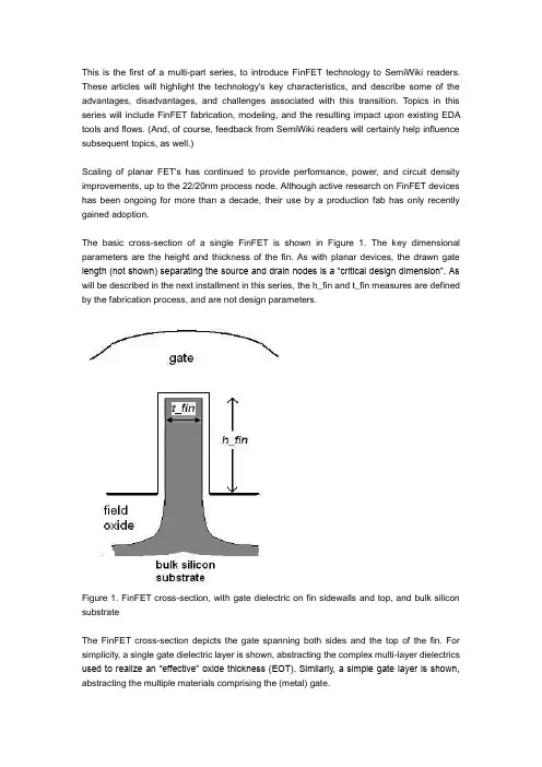
This is the first of a multi-part series, to introduce FinFET technology to SemiWiki readers. These articles will highlight the technology's key characteristics, and describe some of the advantages, disadvantages, and challenges associated with this transition. Topics in this series will include FinFET fabrication, modeling, and the resulting impact upon existing EDA tools and flows. (And, of course, feedback from SemiWiki readers will certainly help influence subsequent topics, as well.)Scaling of planar FET's has continued to provide performance, power, and circuit density improvements, up to the 22/20nm process node. Although active research on FinFET devices has been ongoing for more than a decade, their use by a production fab has only recently gained adoption.The basic cross-section of a single FinFET is shown in Figure 1. The key dimensional parameters are the height and thickness of the fin. As with planar devices, the drawn gate length (not shown) separating the source and drain nodes is a “critical design dimension”. As will be described in the next installment in this series, the h_fin and t_fin measures are defined by the fabrication process, and are not design parameters.Figure 1. FinFET cross-section, with gate dielectric on fin sidewalls and top, and bulk silicon substrateThe FinFET cross-section depicts the gate spanning both sides and the top of the fin. For simplicity, a single gate dielectric layer is shown, abstracting the complex multi-layer dielectrics used to realize an “effective” oxide thickness (EOT). Similarly, a simple gate layer is shown, abstracting the multiple materials comprising the (metal) gate.In the research literature, FinFET's have also been fabricated with a thick dielectric layer on top, limiting the gate's electrostatic control on the fin silicon to just the sidewalls. Some researchers have even fabricated independent gate signals, one for each fin sidewall – in this case, one gate is the device input and the other provides the equivalent of FET “back bias” control.For the remainder of this series, the discussion will focus on the gate configuration shown, with a thin gate dielectric on three sides. (Intel denotes this as “Tri-Gate” in their recent IvyBridge product announcements.) Due to the more complex fabrication steps (and costs) of “dual-gate” and “independent-gate” devices, the e xpectation is that these alternatives will not reach high volume production, despite some of their unique electrical characteristics.Another fabrication alternative is to provide an SOI substrate for the fin, rather than the bulk silicon substrate shown in the figure. In this series, the focus will be on bulk FinFET's, although differences between bulk and SOI substrate fabrication will be highlighted in several examples.Figure 2. Multiple fins in parallel spaced s_fin apart, common gate inputFigure 2 illustrates a cross-section of multiple fins connected in parallel, with a continuous gate material spanning the fins. The Source and Drain nodes of the parallel fins are not visible in this cross-section – subsequent figures will show the layout and cross-section view of parallel S/D connections. The use of parallel fins to provide higher drive current introduces a third parameter, the local fin spacing (s_fin).Simplistically, the effective device width of a single fin is: (2*h_fin + t_fin), the total measure of the gate's electrostatic control over the silicon channel. The goal of the fabrication process would be to enable a small fin spacing, so that the FinFET exceeds the device width that a planar FET process would otherwise provide:s_fin < (2*h_fin + t_fin)Subsequent discussions in this series will review some of the unique characteristics of FinFET's, which result in behavior that differs from the simple (2*h + t) channel surface current width multiplier.The ideal topology of a “tall, narrow” fin for optimum circuit density is mitigated by the difficulties and variations associated with fabricating a high aspect ratio fin. In practice, an aspect ratio of (h_fin/t_fin ~2:1) is more realistic.One immediate consequence of FinFET circuit design is that the increments of device width are limited to (2h + t), by adding another fin in parallel. Actually, due to the unique means by which fins are patterned, a common device width increment will be (2*(2h+t)), as will be discussed in the next installment in this series.The quantization of device width in FinFET circuit design is definitely different than the continuous values available with planar technology. However, most logic cells already use limited device widths anyway, and custom circuit optimization algorithms typically support “snapping” to a fixed set of available width values. SRAM arrays and analog circuits are the most impacted by the quantized widths of FinFET's – especially SRAM bit cells, where high layout density and robust readability/writeability criteria both need to be satisfied.The underlying bulk silicon substrate from which the fin is fabricated is typically undoped (i.e., a very low impurity concentration per cm**3). The switching input threshold voltage of the FinFET device (Vt) is set by the workfunction potential differences between the gate, dielectric, and (undoped) silicon materials.Although the silicon fin impurity concentration is effectively undoped, the process needs to introduce impurities under the fin as a channel stop, to block “punchthrough” current between source and drain nodes from carriers not controlled electrostatically by the gate input. The optimum means of introducing the punchthrough-stop impurity region below the fin, without substantially perturbing the (undoped) concentration in the fin volume itself, is an active area of process development.Modern chip designs expect to have multiple Vt device offerings available –e.g., a “standard” Vt, a “high” Vt, and a “low” Vt – to enable cell-swap optimizations that trade-off performance versus (leakage) power. For example, the delay of an SVT-based logic circuit path could be improved by selectively introducing LVT-based cells, at the expense of higher power. In planar fabrication technologies, multiple Vt device offerings are readily available, using a set ofthreshold-adjusting impurity implants into masked channel regions. In FinFET technologies, different device thresholds would be provided by an alternative gate metallurgy, with different workfunction potentials.The availability of multiple (nFET and pFET) device thresholds is a good example of the tradeoffs between FinFET's and planar devices. In a planar technology, the cost of additional threshold offerings is relatively low, as the cost of an additional masking step and implant is straightforward. However, the manufacturing variation in planar device Vt's due to “channel random dopant fluctuation” (RDF) from the implants is high. For FinFET's, the cost of additional gate metallurgy processing for multiple Vt's is higher – yet, no impurity introduction into the channel is required, and thus, little RDF-based variation is measured. (Cost, performance, and statistical variation comparisons will come up on several occasions in this series of articles.)The low impurity concentration in the fin also results in less channel scattering when the device is active, improving the carrier mobility and device current.Conversely, FinFET's introduce other sources of variation, not present with planar devices. The fin edge “roughness” will result in variation in device Vt and drive current. (Chemical etch steps that are selective to the specific silicon crystal surface orientation of the fin sidewall are used to help reduce roughness.)The characteristics of both planar and FinFET devices depend upon Gate Edge Roughness, as well. The fabrication of the gate traversing the topology over and between fins will increase the GER variation for FinFET devices, as shown in Figure 3.Figure 3. SEM cross-section of multiple fins. Gate edge roughness over the fin is highlighted in the expanded inset picture. From Baravelli, et al, “Impact of Line Edge Roughness and Random Dopant Fluctuation on FinFET Matching Performance”, IEEE Transactions on Nanotechnology, v.7(3), May 2008.The next entry in this series will discuss some of the unique fabrication steps for FinFET's, andhow these steps influence design, layout, and Design for Manufacturability:Introduction to FinFET technology Part IIThe major process steps in fabricating silicon fins are shown in Figures 1 through 3. The step that defines the fin thickness uses Sidewall Image Transfer (SIT). Low-pressure chemical vapor (isotropic) deposition provides a unique dielectric profile on the sidewalls of the sacrificial patterned line. A subsequent (anisotropic) etch of the dielectric retains the sidewall material (Figure 1). Reactive ion etching of the sacrificial line and the exposed substrate results in silicon pedestals (Figure 2). Deposition of a dielectric to completely fill the volume between pedestals is followed by a controlled etch-back to expose the fins (Figure 3).Figure 1. Cross-section of sidewalls on sacrificial lines after CVD etch.Figure 2. Cross-section of silicon pedestals after RIE etch, using Sidewall Image Transfer.Figure 3. Cross-section of silicon fins after oxide deposition and etch-back, and gate deposition.Low-pressure dielectric deposition to create sidewalls on a polysilicon line is a well-known technique – it is commonly used to separate (deep) source/drain implant areas from the planar FET transistor channel. FinFET fabrication extends this technique to pattern definition for silicon fin etching.There is no photolithography step associated with SIT, just the patterning of the sacrificial lines. As a result, the fin thickness can be smaller than the photolithographic minimum dimensions. The fin thickness is defined by well-controlled dielectric deposition and etching steps rather than photoresist patterning, reducing the manufacturing variation. However, there is variation in fin height, resulting from (local) variations in the etch-back rate of dielectric removal. (For FinFET's on an SOI substrate, the fin height is defined by the silicon layer thickness, with a 'natural' silicon etch-stop at the insulator interface in contrast to the timed-etch fin height for bulk substrate pedestals.)There are several characteristics to note about SIT technology. Nominally, fins come in pairs from the two sidewalls of the sacrificial line. Adding fins in parallel to increase drive current typically involves adding a pair of fins: delta_w = (2*(2*h_fin + t_fin)).To “cut” fins, a masked silicon etching step is required. There are two considerations for cutting fins. The first involves breaking long fins into individual pairs. The other is to create an isolated fin, by removing its SIT-generated neighbor. Critical circuits that require high density and/or different device sizing ratios may justify the need for isolated fin patterning – e.g., SRAM bit cells. Compared to cutting, isolated fin patterning may involve different design rules and separate (critical) lithography steps, and thus additional costs.Additional process steps are required to introduce impurities of the appropriate type below the fin to provide a punchthrough stop (PTS), ensuring there is no direct current path between drain and source that is not electrostatically controlled by the gate input.The dielectric between pedestals that remains after etch-back serves as the field oxide, asdenoted in Figure 3. The gate material traversing between parallel fins is well-separated from the substrate, minimizing the Cgx parasitic capacitance.The uniformity and control of the final fin dimensions are important process characteristics, for both the fin thickness and fin corner profiles. (The profile of the pedestal below the fin is less critical, and may be quite tapered, as shown in Figure 3.) Tolerances in the fin thickness arise from variations in the vertical, anisotropic SIT silicon etch. The fin thickness at the bottom is also dependent upon the uniformity of the etch-back – the goal is to minimize any dielectric “foot” remaining at the bottom of the fin.As will be discussed in the next series installment, variations in t_fin have significant impact upon the transistor model. The top corner profiles also have an impact upon the transistor behavior, as the electric fields from the gate to the silicon fin are concentrated in this region, originating from both the sidewall and top gate materials.Gate patterning follows conventional photolithographic steps, although the recent introduction of metal gate materials has certainly added to the complexity, especially as the gate must now traverse conformally over parallel fins. As with a planar FET technology, the gate length is the 'critical dimension' that is typically quoted as the basis for the process node – e.g., 20nm.In contrast to planar FET technologies, providing multiple FinFET threshold voltage (Vt) offerings requires significant additional process engineering. The threshold of any FET is a function of the workfunction potential differences between the gate, dielectric, and silicon substrate interfaces. In planar FET's, multiple Vt offerings are readily provided by shallow (masked) impurity implants into the substrate prior to gate deposition, adjusting the workfunction potential between dielectric and channel. However, the variation in the (very small) dosage of impurities introduced in the planar channel results in significant Vt variation, due to 'random dopant fluctuation' (RDF).With FinFET's, there is ongoing process development to provide different metal gate compositions (and thus, metal-to-dielectric workfunctions) as the preferred method for Vt adjust. The advantage of using multiple gate metals will be to reduce the RDF source of Vt variation substantially, as compared to implanting a (very, very small) impurity dosage into the fin volume. The disadvantage is the additional process complexity and cost of providing multiple metal gate compositions.Another key FinFET process technology development is the fabrication of the source/drain regions. As was mentioned in the first series installment, the silicon fin is effectively undoped. Although advantageous for the device characteristics, the undoped fin results in high series resistance outside the transistor channel, which would otherwise negate the drive current benefits of the FinFET topology.To reduce the Rs and Rd parasitics, a spacer oxide is deposited on the FinFET gate sidewalls, in the same manner as sidewalls were patterned earlier for SIT fin etching. To increase thevolume of the source/drain, a 'silicon epitaxy growth' (SEG) step is used. The exposed S/D regions of the ori ginal fin serve as the “seed” for epitaxial growth, separated from the FinFET gate by the sidewall spacer. Figure 4 shows the source/drain cross-section after the SEG step.Figure 4. Cross section of source/drain region, after epitaxial growth. Original fin is in blue -- note the faceted growth volume. The current density in the S/D past the device channel to the silicide top is very non-uniform. From Kawasaki, et al, IEDM 2009, p. 289-292.The incorporation of impurities of the appropriate type (for nFET or pFET) during epitaxial growth reduces the S/D resistivity to a more tolerable level. The resistivity is further reduced by silicidation of the top of the S/D region. In the case of pFET's, the incorporation of a small % of Ge during this epitaxy step transfers silicon crystal stress to the channel, increasing hole carrier mobility significantly.Raised S/D epitaxy has been used to reduce Rs/Rd for planar FET's, as well. However, there are a couple of interesting characteristics to FinFET S/D process engineering, due to the nature of the exposed fin S/D nodes, compared to a planar surface.The epitaxial growth from the exposed crystalline surface of the silicon fin results in a “faceted” volume for the S/D regions. Depending upon the fin spacing and the amount of epitaxial growth, the S/D regions of parallel fins could remain isolated, or could potentially “merge” into a continuous volume. The topography of the top surface for subsequent metallization coverage is very uneven. The current distribution in the S/D nodes outside the channel (and thus, the effective Rs and Rd) is quite complex.FinFET's could be fabricated with either a HKMG 'gate-first' or a 'gate-last' process, although gate-last is likely to be the prevalent option. In a gate-last sequence, a dummy polysilicon gate is initially patterned and used for S/D formation, then the gate is removed and the replacement metal gate composition is patterned.FinFET's also require a unique process step after gate patterning and S/D node formation, to suitably fill the three-dimensional “grid” of parallel fins and series gates with a robust (low K) dielectric material.Contacts to the S/D (and gate) will leverage the local interconnect metallization layer that has recently been added for planar 20nm technologies.The next installment of this series will discuss some of the unique FinFET transistor modeling requirements./forum/content/1228-introduction-finfet-technology-part-ii.html。

Is My Child Ready for School?A practical guidefor parents©2014 Lakeshore S82134 Preschool 4 Pre-K4 KindergartenWhen children enter preschool, prekindergarten and kindergarten programs, they are expected to have certain basic skills, which are often referred to as school-readiness skills. These skills cover a wide range of topics within the following subject areas:4 Language and Literacy4 Math4 Critical Thinking and Problem Solving4 Social and Emotional Development4F ine Motor Development, IncludingDressing Skills To help your child develop age-appropriate skills within these categories—and fully prepare for school—we’ve created this easy-reference guide. It includes a handy checklist showing the skills children should have when entering preschool, prekindergarten or kindergarten programs—so you can check off each skill as your child masters it.We’ve also included product suggestions to help children reach their goals—and have a fun and successfulschool year! Find our full selection ofproducts to prepare kids for schoolat .Help children develop skills for success in school!q P ut away toys on his/her own q L isten to simple instructions q R ecognize others’ emotionsq T ake turns and share toys q S it still during a story q E xpress thoughtsand needs verbally, with a growing vocabulary q D ress himself/herself q S tring large beadsq R ecognize some shapes and colors q D raw with crayons or pencils q R ecite his/her full nameqV erbally count from 1 to 5 q R ecite the alphabetand recognize some letters q E ngage in pretend playEntering PreschoolBest-Buy Kitchen Playset P r e s c P r e s c Magnetic Color MazeChicka Chicka Boom Boom Activity Tree and BookPeg-A-Picture BoardsComplete SetJJ453LA645BK647LA427q K ick and throw a ball q C ut with scissors q K now his/her own birthday, address and phone number q V erbally count from 1 to 10q R ecognize and name numerals 1–5q R ecognize and name the following shapes: square, circle, rectangle, triangle and oval q R ecognize and name the following colors: red, orange, yellow, green, blue, purple, brown, black and white q F ollow simple two-step directions q I dentify simple patterns (e.g., red, blue, red, blue, red, blue)q P lace objects in two or more groups based on their differences (e.g., by color, size or shape) q C ompare and order objects in relation to size or length (e.g., place blocks side by side in size order, from smallest to largest)q R ecognize some letters (especially those in their own name)q I dentify the sounds of a few letters q R etell simple stories and nursery rhymes q A sk and answer questions about storiesEntering Pre-KP r e Early Math Activity CenterP r e Button Sorting CenterTabletop Hardwood BlocksFarm Sorting CenterSound Phone CenterLA278EE525JJ779BC301FF186Products to Support Reaching GoalsqA ttempt to tie his/her shoes qB egin to hold a pencil correctly qC atch a large ball with both hands q R ecognize and name most uppercase and lowercase letters q P roduce the correct sound for 10–20 letters q R ecognize his/her name in print q R etell simple stories in proper sequence (e.g., The Three Little Pigs)q I dentify simple rhymes (e.g., cat and hat)q R ecognize and name numerals 1–10q C ount up to 10 objects using one-to-one correspondence(e.g., count one object per number)q U se like objects to measure and compare lengths (e.g., measure objects using cubes or links)q U nderstand the use of ordinal numbers (e.g., first, second and third)q U nderstand general time concepts (e.g., yesterday, today, tomorrow and last week)What Y our Child Should Know/Do When Entering KindergartenK i n d e r g a r t e nK i n d e r g a r t e nMath LinksSorting KitThe Three Little Pigs Storytelling Puppet SetAlphabet Mystery Box JJ157GG167TT625RA683FF315Join us every Saturday... FREE CRAFTS FOR KIDS!Sign up and SAVE! Receive Lakeshore text messages, and be the first to learn about...from 11 a.m. to 3 p.m.4S pecial discounts4M oney-saving coupons4F un in-store eventsLakeshore gift cards...give the perfect gift!Ask a store associate for details.Available at the register.m e!。

ReviewCombustion characteristics and emissions of Fischer e Tropsch diesel fuels in IC enginesS.S.Gill a ,A.Tsolakis a ,*,K.D.Dearn a ,J.Rodríguez-Fernández ba School of Mechanical Engineering,University of Birmingham,Birmingham B152TT,UKbE.T.S.Ingenieros Industriales,Dpto.Mecánica Aplicada e Ingeniería de Proyectos,Universidad de Castilla-La Mancha,13071Ciudad Real,Spaina r t i c l e i n f oArticle history:Received 3August 2010Accepted 8September 2010Available online 25October 2010Keywords:Diesel engines Fischer e Tropsch Combustion EmissionsCetane numbera b s t r a c tThis article gives a condensed overview of Gas-to-Liquid (GTL),Biomass-to-Liquid (BTL)and Coal-to-Liquid (CTL)theory and technology by the use of Fischer e Tropsch (F e T)processes.Variations of the F e T process can be used to tailor the fuel properties to meet end user needs as well as aid vehicle manu-facturers in achieving forthcoming emission regulations.They do this by improving engine-out emissions and exhaust gas after-treatment performance.Regardless of feedstock or process,F e T diesel fuels typically have a number of very desirable properties,including a very high cetane number.This review focuses on how fuel properties impact pollutant emissions and draws together data from various studies that have been carried out over the past few years.Reduced emission levels as demonstrated in several publications have been attributed to several chemical and physical characteristics of the F e T diesel fuels including reduced density,ultra-low sulfur levels,low aromatic content and high cetane rating,but not all of them contribute to the same extent to the emissions reduction.Ó2010Elsevier Ltd.All rights reserved.Contents 1.Introduction ......................................................................................................................5041.1.Fuel crisis ..................................................................................................................5041.2.Diesel engines and emissions .................................................................................................5041.3.Emission standards for vehicles e transport sector ..............................................................................5041.4.Fischer e Tropsch diesel fuels ..................................................................................................5051.5.Well-to-wheels analysis of fuels ...............................................................................................5071.6.Effect of fuel properties on engine emissions ...................................................................................5082.Gas-to-liquid (GTL)...............................................................................................................5082.1.Introduction .................................................................................................................5082.2.GTL fuels combustion and emissions characteristics (509)2.2.1.Mechanically-injected and electronic pump-line-nozzle systems mon-rail systems (512)2.3.Engine optimization-emission strategies with GTL fuels ..........................................................................5153.Biomass-to-liquid (BTL)............................................................................................................5173.1.Introduction .................................................................................................................5173.2.BTL fuels combustion and emissions characteristics ..............................................................................5174.Coal-to-liquid (CTL)...............................................................................................................5204.1.Introduction .................................................................................................................5204.2.CTL fuels characteristics .....................................................................................................5205.Summary of Fischer e Tropsch diesel fuels ............................................................................................5206.Conclusion .......................................................................................................................520Acknowledgments ................................................................................................................521References (521)*Corresponding author.Tel.:þ44(0)1214144170;fax:þ44(0)1214147484.E-mail address:a.tsolakis@ (A.Tsolakis).Contents lists available at ScienceDirectProgress in Energy and Combustion Sciencejournal homepage:w ww.el/locate/pecs0360-1285/$e see front matter Ó2010Elsevier Ltd.All rights reserved.doi:10.1016/j.pecs.2010.09.001Progress in Energy and Combustion Science 37(2011)503e 5231.Introduction1.1.Fuel crisisThe world is presently confronted with the twin crises of fossil-fuel depletion and environmental degradation.Excessive use of fossil fuels has major local,regional and global environmental impacts[1]:1.Local e Air pollution2.Regional e Acid rain and airborne pathogens(i.e.infections,particles and chemicals)3.Global e Greenhouse effectProjections for the30-year period from1990to2020indicate that vehicle travel,and consequently fossil-fuel demand,will almost triple and the resulting emissions will pose a serious problem.The main reason for increased pollution levels,in spite of the stringent emission standards that have been enforced,is the increased demand for energy in all sectors and most significantly the increased use of automobiles[1].1.2.Diesel engines and emissionsAlthough,the diesel engine is an attractive solution for carbon dioxide(CO2)reduction,there remains a challenge to control simultaneously nitrogen oxides(NO x)and particulate matter(PM) emissions to a level required by prevailing regulations[2,3]. Unfortunately,if the diesel combustion system is not well controlled,it can produce higher levels of PM and/or NO x.PM, which is composed of soot and sulfate bound with water and unburned oil and fuel,can have associated health issues.Whereas NO x,which is formed by oxidation of atmospheric and/or fuel contained nitrogen at high temperatures in the power cylinder,is capable of producing smog and acid rain,polluting waterways and crops[4].Since NO x and PM emissions from current diesel technologies are close to the limits permitted by regulations and both limits will become more stringent in the near future;these two emissions will be critical factors in the development of new diesel engines.An improved knowledge of the potential to reduce these types of emissions could help engine manufacturers adapt their engines to the use of biofuels and to optimize them.This can be done by readjusting the compromise between efficiency,costs(mainly due to after-treatment systems)and emissions within the regulation limits[5].However as engines are currently calibrated to be as efficient as possible while complying with the emission standards, there still stands a trade-off between the emissions performance and efficiency.Among other solutions to reduce both NO x and PM such as reformed exhaust gas recirculation(REGR),selective cata-lytic reduction(SCR)catalysts,and diesel particulatefilters(DPF), alternative fuels like biofuels and designed fuels such as Fischer e Tropsch(F e T)diesel fuels appear to be the feasible short term solution[3].There are two strands to the European Legislation which promote the use of biofuels,namely article7a of the Fuels Quality Directive and the Renewable Energy Directive.The European directive2009/ 30/EC was adopted to revise the Fuel Quality Directive98/70/EC. Apart from establishing the target aiming to satisfy10%of its transport fuel needs from renewable sources,it introduces a requirement of fuel suppliers to reduce the greenhouse gas(GHG) intensity of energy supplied for road transport in article7a[6].The European Union(EU)Renewable Energy Directive sets out a path targeting15%of energy from renewable sources by2020[7].With ongoing improvements aimed at enhancing performance and reducing noise and emissions,the diesel engine has become an increasingly attractive option for passenger car applications[3]. 1.3.Emission standards for vehicles e transport sectorUnder the framework of the European Climate Change Pro-gramme,the European Commission set a goal of reducing CO2 emissions from new passenger cars and light commercial vehicles. Afleet-average CO2emission target of130g/km for new passenger cars must be reached by each vehicle manufacturer by2015,using vehicle technology under the Regulation443/2009/EC.However to meet the EU CO2target of120g/km,a further10g/km is to be provided through additional measures such as biofuels[8].The proposed legislation to reduce the CO2emissions from light commercial vehicles[COM(2009)593]introduces afleet-average CO2emission target of175g/km fully phased-in by2016.This regulation is applicable to vehicles category N1(light commercial vehicles)with a reference mass not exceeding2610kg[9].Euro6stage has been adopted at the same time as Euro5,but will lay down significantly lower limits for NO x emissions from diesel cars[10].The Euro6Stage European emission regulations for light passenger and commercial vehicles were introduced by Regulation(EC)No715/2007later amended by the Commission regulation(EC)No.692/2008of July2008.All vehicles equipped with a diesel engine will be required to substantially reduce their emissions of NO x for the Euro6regulation to be introduced on1st September2014for the approval of vehicles,and from1st January 2015for the registration and sale of new types of cars.As illustrated in Table1,NO x emissions from passenger cars and light commercial vehicles(category N1,class I)intended to be used for transport will be capped at80mg/km(an additional reduction of more than50% compared to the Euro5standard)[12].For the other regulated emissions,such as the control of carbon monoxide(CO)and total hydrocarbon(THC),although not in engines,would probably be required to meet future limits as a result of developments in after-treatment systems.This is especially the case if low-temperature combustion modes are used(for example late injection,high EGR ratios etc).In the case of PM,Euro6will not reduce the emissions compared to the levels imposed by Euro5,but the latter has alreadyTable1Euro6emission regulations for light passenger and commercial vehicles(after[11]).Compression ignition(CI)limit valuesMass of carbon monoxide(CO) (mg/km)Mass of oxidesof nitrogen(NO x)(mg/km)Combined massof hydrocarbonsand oxides of nitrogen(THCþNO x)(mg/km)Mass of particulatematter(PM)(mg/km)Number of particles(P)(#/km)Vehicle Type Category ClassPassenger cars All M e50080170 5.0/4.5 6.0Â10Light commercial vehicles1305kg N1I50080170 5.0/4.5 6.0Â1011 1305e1760kg II630105195 5.0/4.5 6.0Â1011 >1760kg(Max3500kg)III740125215 5.0/4.5 6.0Â1011 S.S.Gill et al./Progress in Energy and Combustion Science37(2011)503e523504forced the manufacturers to introduce DPF in vehicles.Inversely, the NO x after-treatment techniques associated with heavy-duty diesel have already been implemented in order to meet the Euro V limits,while Euro VI will mainly imply an effort to reduce PM emissions.European emission regulations(see Table2)for new heavy-duty engines,which generally include trucks and buses, were introduced by Regulation595/2009,published in July2009.It is worth noting that for passenger and light commercial vehicles,the standards are defined in mg/km,while for heavy-duty vehicles they are defined by engine power,mg/kWh,and are therefore not directly comparable.Fig.1gives an overview of the European emission standards which stage the progressive intro-duction of increasingly stringent standards.In addition to this Fig.2 gives a brief summary of the emission standards implemented in China and the United States.The Chinese standards are based on European regulations with a certain time delay.The US standards for engines and emissions are established by the US Environmental Protection Agency(EPA)[14].1.4.Fischer e Tropsch diesel fuelsDue to the concern about the limited future oil resources and requirement of CO2reduction,interests in renewable and alternative fuels have grown increasingly.New diesel fuels are necessary not only to improve engine performance and emissions,but also to ensure the sustainability of the fuel supplies.The chronogram in Fig.3shows the number of publications related to F e T process fuels, which is then illustrated in terms of individual raw materials.There seems to be an overall exponential increase especially in work related to F e T and its processes for new alternative fuels.However studies related to BTL and CTL fuels have successively been low, whereas GTL type fuels have become more attractive.The following work focuses on current studies carried out with second generation F e T diesel fuels,and is a good reflection of the literature selected from amongst the most representative studies published in journals.Ultra-clean,high cetane number fuels(facilitating lower combustion temperatures and pressures)derived from an F e T process(final liquid fuel to be obtained from renewable sources)is a promising alternative[3,16].They are virtually free of sulfur and aromatic hydrocarbons(HC),can facilitate further reduction of engine-out emissions,and improve the performance of the cata-lytic after-treatments and fuel reformers[3].These fuels show a very high potential for realizing a much more favorable NO x/PM trade-off without the commonly observed associated penalties in fuel efficiency[17].The raw material can either be natural gas(the final liquid fuel being GTL),coal(CTL)or residual biomass(BTL).GTL is already produced commercially and diesel fuels blended with GTL are available in several European countries[18].A number of new large-scale GTL production plants is currently being planned or under construction,resulting in a potential total GTL diesel fuel production of significant volumes(1million barrels/day or more) within the next decade[19].The exhaust emissions performance of GTL diesel fuels has been the subject of a growing number of technical publications in recent years.The basic technology is known as the Fischer e Tropsch process and a number of companies have developed this synthetic process using catalytic technology.The resulting synthesized straight-chain HC has good compression ignitability and are suitable for use with automobiles as diesel engine fuel.For this reason,many reports have been published concerning the influence of F e T diesel fuel properties on diesel emissions characteristics[20].Franz Fischer and Hans Tropsch developed the process that bears their names in the1920’s.The production of diesel fuels using the F e T process is a set of chemical reactions in the presence of a catalyst[21]:Synthesis Gas(Syngas)FormationCH nþO2/12n H2þCO(1) F e T Synthesis Processn COþð2nþ1ÞH2/C n H2nþ2þn H2O Paraffin’s(2) n COþ2n H2/C n H2nþn H2O Olefins(3)Synthesis gas can be formed from any carbonaceous material such as natural gas,coal,or biomass.Several reactions are required to obtain the gaseous reactants required for F e T catalysis.Reactant gases entering an F e T reactor mustfirst be desulfurized to protect the catalysts that are readily poisoned.The following major sets of reactions are employed to adjust the H2/CO ratio:Water-Gas-Shift Reaction e Provides a source of hydrogen(H2): H2OþCO/H2þCO2(4)Steam Reforming is important for those F e T plants that start with methane:H2OþCH4/COþ3H2(5)Several routes are possible for the formation of synthesis gas from natural gas,including autothermal reforming,steam reforming (Reaction(5)),and partial oxidation.The formation of synthesis gas from coal or biomass is called gasification,wherein the feedstock is reacted with steam and oxygen(O2).The next step in the F e T production process is the conversion of synthesis gas into HC.This begins with H2and CO molecules being formed into e CH2e alkyl radicals and water in an exothermic reaction.The e CH2e radicals then immediately combine in an iron or cobalt catalytic reaction to make synthetic olefin and/or paraffin HC(Reactions(2)and(3))of various chain-lengths(high boiling point wax and olefinic naphtha). The selectivity(the amount of desired product obtained per unit consumed reactant)is influenced by parameters such as tempera-ture,H2/CO ratio in the feed gas,pressure and the catalyst type.The F e T product can be upgraded to high quality diesel fuel through post-processing and any oxygenates formed during theTable2Euro VI emission regulations for heavy-duty diesel engines(after[13]).Compression ignition(CI)limit valuesMass of carbon monoxide(CO) (mg/kWh)Mass of totalhydrocarbons(THC)(mg/kWh)Mass of oxidesof nitrogen(NO x)(mg/kWh)Ammonia(NH3)(ppm)Mass of particulatematter(PM)(mg/kWh)European steadystate cycle(ESC)15001304001010European transient cycle(ETC)40001604001010S.S.Gill et al./Progress in Energy and Combustion Science37(2011)503e523505F e T process are often removed during this step.Addition of H 2and a catalyst causes hydrocracking,rupturing long carbon chains into shorter,liquid parts to produce cuts that correspond to a range of conventional re finery products.Regardless of feedstock or process,F e T diesel fuels typically have a number of very desirable proper-ties [22].Fig.4gives a simple overview of the F e T technology.Adaptation of the F e T synthesis to syngas of different origins revolves around purity,cleanliness and the H 2/CO ratio of the gas [23].It is important to note that the distillation range of F e T diesel can be customized by F e T synthesis conditions and by the distil-lation cut after synthesis occurs.Therefore this is not an inherent property of the F e T diesel.A variety of catalysts can be used for the F e T process,but the most common are the transition metals,cobalt and iron.Cobalt catalysts are more active for F e T synthesis when the feedstock is natural gas.Natural gas has high H 2/CO ratio,so the water-gas-shift is not needed for cobalt catalysts.Iron catalysts are preferred for lower quality feed-stocks such as coal or biomass.F e T synthesis is technically classi fied into two categories,the high-temperature Fischer e Tropsch (HTFT)and the low-temperature Fischer e Tropsch (LTFT)processes.The criterion for this classi fication is the operating temperature of the synthesis,which ranges between 310e 340 C for the HTFT process and 210e 260 C for the LTFT process [25,26].The F e T syncrude composition and its distillate yields are mainly determined by the catalyst type (iron or cobalt based)and the reaction conditions.The carbon number distribution of an HTFT and LTFTsynthesis product is different.HTFTsyncrude has a high naphtha yield and low contents of material boiling above 360 C,whereas a synthesis product from the LTFT process consists of a considerable amount of higher-boiling HC.Also the final distillate yield isFig.2.Overview of emission standards for China and United States [14].Fig.1.European emission standards comparison for,a)Diesel passenger cars b)Heavy-duty diesel engines [15].S.S.Gill et al./Progress in Energy and Combustion Science 37(2011)503e 523506substantially larger for the LTFT process.But a key difference of HTFT and LTFT is thefinal composition,being HTFT mainly composed of aromatics and olefins and LTFTof paraffin’s.As a consequence,HTFT is apparently more suitable as a gasoline fuel due to the high octane number of aromatics,whereas LTFT is used for diesel fuels(high cetane number of paraffinic compounds,but with a density usually below the diesel standards)[25].However,good ignitability(i.e.high cetane number)is crucial for a diesel fuel,and constitutes the feature that reinforces the introduction of F e T derived fuels in the market, while density issues do not introduce severe limitations(at least in the typical ranges).F e T diesel fuels can be designed to have a high cetane number, low aromatics,thus low C/H ratio and relatively low specific gravity. These fuels are also extremely low in sulfur(often less than1ppm) when derived from natural gas.These particular fuels are a strong candidate for fuel blending and as a neat fuel in transportation markets.Their impact on after-treatment catalyst development and particulate abatement is attractive due to their low sulfur content, absence of aromatic HC and high H2content[2,27].However,some properties of F e T diesel fuels are still to be improved.Poly-aromatic and sulfur compounds contribute to the lubricity of diesel fuels, although sulfur content in diesel fuels is being virtually eliminated. The very low aromatic content of F e T diesel fuel combined with the near zero sulfur content results in a fuel with poor lubricity prop-erties.Lubricity tests with neat F e T diesel fuels reveal results well below accepted lubricity standards,but not significantly below the US8,EU and MK1diesel fuels(i.e.before additive addition)which consist of sulfur content below10ppm.The lubricity of F e T diesel fuels can be improved to acceptable levels using commercial additives.Fatty acid methyl esters(i.e.biodiesel)can also be used to improve the lubricity of F e T diesel fuel[22].Density is an impor-tant factor for fuel consumption,whereas the other properties mentioned have an effect on emissions.Although density is not a problem for aromatic-containing HTFT diesel,LTFT diesel contains virtually no aromatics and the resulting density of770e780kg/m3 poses a refining challenge.However,synthetic LTFT distillate is increasingly blended into top quality diesel fuels to reduce emis-sions in modern high performance diesel engines[25].Ideally,a compression ignition(CI)fuel would be renewable, produce useable power to current diesel standards,run in both existing and newly manufactured engines and require no engine modifications.In addition,its combustion should produce fewer emissions which would enhance the efficiency of exhaust gas after-treatment systems primarily by increasing the availability of active catalytic sites.In a modern diesel engine synthetic fuels can satisfy many of the above ideal fuel requirements.Recent studies have shown that synthetic fuels have emission benefits in the reduction of HC,CO,NO x and PM.However the density of synthetic fuels such as GTL is lower than that of the standard European specifications for diesel.As a result the volumetric energy density is also lower and the injection system hardware and injection strategy may need to be reconfigured[17,28].1.5.Well-to-wheels analysis of fuelsThe well-to-wheels(WTW)analysis in Fig.5taken from the EU commission WTW report represents the specific life cycle assess-ment of the efficiency of fuels for road transport.The GHG bars represent the combined well-to-tank(WTT)and tank-to-wheels (TTW)stages.As shown in Fig.5,the energy inputs of synthetic fuels are higher than those of conventional diesel.The GHG emis-sions from GTL are slightly higher than those of conventional diesel. CTL diesel produces considerably more GHG emissions,while synthetic diesel from biomass is significantly lower.Though the BTL approach requires a substantial amount of energy,however they have the potential to save more GHG emissions than current biofuel options.The wood pathways produce very little GHG as the conversion process is fuelled by the wood itself although it is notHNatural GasBiomassAirFig.4.F e T technology[24].Fig. 3.Chronogram of published papers related to F e T diesel fuels(ISI web ofknowledge).S.S.Gill et al./Progress in Energy and Combustion Science37(2011)503e523507particularly energy ef ficient.Overall the combined process of primary energy conversion and F e T synthesis is energy-intensive,especially for coal and wood though less so for natural gas.This is primarily due to the overall process with gas being more straight-forward and more energy ef ficient.However the CTL schemes are attracting a lot of interest,particularly in combination with CO 2capture and storage [23].1.6.Effect of fuel properties on engine emissionsSome of the physical and chemical properties of the F e T fuels are behind their potential to reduce engine-out emissions.Among these properties,the higher cetane number is the most cited to justify the trends [3,17,20],but others such as the differences in aromatic content or the adiabatic flame temperature play a role as well.Sulfur content or volatility,which could affect emissions,is a marginal consideration as sulfur content is being eradicated from all types of diesel fuels [5].Differences in volatility are uncertain,since this property is strongly affected by the oil-fraction that is used in the manufacturing process of both conventional and F e T diesel fuels.The cetane number affects engine performance and emissions through the chemical ignition delay.The higher the cetane number,the lower this delay,thus the fraction of injected fuel that is burnt under pre-mixed conditions is reduced.Pre-mixed combustion is associated with higher pressures,pressure gradients and temper-atures in the chamber,all of which increase NO x formation.Aromatic compounds are suspected of directly in fluencing the first steps of soot particle formation (for example,the nano-particles inception).The chemical pathway involves especially polycyclic aromatic compounds,but this is a subject under continuous investigation [29,30].Adiabatic flame temperatures of fuels may be calculated from thermodynamic properties,and are directly related to the thermal formation of NO x .Aromatic compounds are reported to have higher adiabatic flame temperatures than paraf finic ones [31].Finally and regarding the sulfur content in fuels,which when oxidized (to form sulfur oxides)combine with water to produce sulphates,a component of the insoluble organic fraction (ISF)of the particulate matter emitted.However,sulfur reduction in recent years has been related to its effect on catalysts (i.e.deactivation,poisoning)rather than increases in particulate.Kidoguchi et al.[32]were one of many research groups who studied the effect of fuel properties on direct injection diesel combustion.The study revealed that by reducing the cetane number,there was an increase in NO x and decrease in PM emissions at high load.This effect was thought to be due to the low cetane number fuel having a long ignition delay causing a high maximum heat release rate and shortened combustion duration.However for low loads,lower cetane fuels produced higher THC due to local over lean mixtures caused by the ignition delay,hence resulting in an incomplete combustion.McMillian and Gautam [27]supports this and concludes THC brake speci fic emissions were reduced for F e T diesel fuels as a direct result of higher cetane number and hence the expected ignition delay.Szybist et al.[33]found a similar relation-ship between NO x and cetane number,however only when the injection timing was advanced.The reductions were thought to be coupled to the lower C/H ratio in the fuel which in turn reduced the flame temperature and hence the ability to produce NO x .When the cetane number was kept constant,changing the aromatic content had little effect on the combustion characteristics,although increasing the aromatic content resulted in high NO x and PM emissions.This was assumed by Kidoguchi et al.[32]to be asso-ciated with the locally rich and high-temperature region formed due to various factors.These may include the high adiabatic flame temperature,the dif ficulty in pyrolysis of HC containing aromatics as well as the slow physical process such as evaporation and turbulent mixing.However as the injection pressure was raised,the effects of cetane number and aromatic content on particulate emissions become less signi ficant.Nishiumi et al.[34]concluded that the narrow distillation characteristics using paraf finic fuels simulating F e T diesel fuel (which eliminates heavy HC fraction)could reduce the soluble organic fraction (SOF)in PM emissions.However the high cetane number promoted the formation of ISF,especially at light load conditions.It was thought that the higher the cetane number the less PM produced as there is a shorter ignition delay and consequently more time for the complete combustion and for particle oxidization.2.Gas-to-liquid (GTL)2.1.IntroductionThe F e T reaction is considered as the heart of the GTL process-chain to produce high quality synthetic liquid HC.The main process steps are illustrated in Fig.6and these include [35]:Synthesis Gas Generation e Synthesis Gas (composed of H 2,CO and CO 2)is produced from natural gas (NG)through areformingFig.5.WTW energy requirement and GHG emissions for synthetic diesel fuel and DME pathways (2010þvehicles)[23].S.S.Gill et al./Progress in Energy and Combustion Science 37(2011)503e 523508。
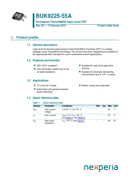
1.Product profile1.1General descriptionLogic level N-channel enhancement mode Field-Effect Transistor (FET) in a plasticpackage using TrenchMOS technology. This product has been designed and qualified to the appropriate AEC standard for use in automotive critical applications.1.2Features and benefits⏹AEC Q101 compliant⏹Low conduction losses due to low on-state resistance⏹Suitable for logic level gate drive sources ⏹Suitable for thermally demanding environments due to 175 °C rating1.3Applications⏹12 V and 24 V loads⏹Automotive and general purpose power switching⏹Motors, lamps and solenoids1.4Quick reference dataBUK9225-55AN-channel TrenchMOS logic level FETRev. 02 — 7 February 2011Product data sheetTable 1.Quick reference data Symbol Parameter ConditionsMin Typ Max UnitV DS drain-source voltage T j ≥25°C; T j ≤175°C --55V I D drain current V GS =5V;T mb =25°C;see Figure 1; see Figure 3--43A P tottotal power dissipationT mb =25°C; see Figure 2--94W2.Pinning information3.Ordering informationStatic characteristicsR DSondrain-source on-state resistanceV GS =4.5V;I D =25A; T j =25°C--27m ΩV GS =10V; I D =25A; T j =25°C-1922m ΩV GS =5V;I D =25A; T j =25°C; see Figure 12;see Figure 13-2125m ΩAvalanche ruggedness E DS(AL)Snon-repetitive drain-source avalanche energyI D =43A; V sup ≤55V; R GS =50Ω; V GS =5V; T j(init)=25°C; unclamped--123mJTable 1.Quick reference data …continued Symbol Parameter ConditionsMin Typ Max Unit Table 2.Pinning information Pin Symbol Description Simplified outline Graphic symbol1G gate SOT428 (DPAK)2D drain 3S sourcembDmounting base; connected to drain32mb1Table 3.Ordering informationType numberPackage NameDescriptionVersion BUK9225-55ADPAKplastic single-ended surface-mounted package (DPAK); 3 leads (one lead cropped)SOT4284.Limiting values[1]peak drain current is limited by chip, not package.Table 4.Limiting valuesIn accordance with the Absolute Maximum Rating System (IEC 60134).Symbol ParameterConditionsMin Max Unit V DS drain-source voltage T j ≥25°C; T j ≤175°C -55V V DGR drain-gate voltage R GS =20k Ω-55V V GS gate-source voltage -1515V I Ddrain currentT mb =25°C; V GS =5V;see Figure 1; see Figure 3-43A T mb =100°C; V GS =5V; see Figure 1-30A I DM peak drain current T mb =25°C; pulsed; t p ≤10µs;see Figure 3[1]-173A P tot total power dissipation T mb =25°C; see Figure 2-94W T stg storage temperature -55175°C T j junction temperature -55175°C Source-drain diodeI S source current T mb =25°C-43A I SM peak source current pulsed; t p ≤10µs; T mb =25°C -173A Avalanche ruggednessE DS(AL)Snon-repetitive drain-source avalanche energyI D =43A; V sup ≤55V; R GS =50Ω; V GS =5V;T j(init)=25°C; unclamped-123mJ5.Thermal characteristicsTable 5.Thermal characteristicsSymbol ParameterConditions Min Typ Max Unit R th(j-mb)thermal resistance from junction to mounting base see Figure 4-- 1.6K/W R th(j-a)thermal resistance from junction to ambient-71.4-K/W6.CharacteristicsTable 6.CharacteristicsSymbol Parameter Conditions Min Typ Max Unit Static characteristicsV(BR)DSS drain-sourcebreakdown voltage I D=0.25mA;V GS=0V; T j=25°C55--V I D=0.25mA;V GS=0V; T j=-55°C50--VV GS(th)gate-source thresholdvoltage I D=1mA; V DS=V GS; T j=25°C;see Figure 111 1.52VI D=1mA; V DS=V GS; T j=-55°C;see Figure 11-- 2.3VI D=1mA; V DS=V GS; T j=175°C;see Figure 110.5--VI DSS drain leakage current V DS=55V;V GS=0V; T j=25°C-0.0510µAV DS=55V;V GS=0V; T j=175°C--500µA I GSS gate leakage current V GS=10V; V DS=0V; T j=25°C-2100nAV GS=-10V;V DS=0V; T j=25°C-2100nAR DSon drain-source on-stateresistance V GS=4.5V;I D=25A;T j=25°C--27mΩV GS=5V;I D=25A;T j=175°C;see Figure 12; see Figure 13--50mΩV GS=10V; I D=25A; T j=25°C-1922mΩV GS=5V;I D=25A;T j=25°C;see Figure 12; see Figure 13-2125mΩDynamic characteristicsC iss input capacitance V GS=0V;V DS=25V; f=1MHz;T j=25°C;see Figure 14-13601724pFC oss output capacitance-240287pF C rss reverse transfercapacitance-160222pFt d(on)turn-on delay time V DS=30V;R L=1.2Ω; V GS=5V;R G(ext)=10Ω; T j=25°C -17-nst r rise time-104-ns t d(off)turn-off delay time-82-ns t f fall time-80-nsL D internal draininductance measured from drain to centre of die;T j=25°C- 2.5-nHL S internal sourceinductance measured from source lead to sourcebond pad; T j=25°C-7.5-nHSource-drain diodeV SD source-drain voltage I S=15A;V GS=0V; T j=25°C;see Figure 15-0.85 1.2Vt rr reverse recovery time I S=20A;dI S/dt=-100A/µs;V GS=-10V;V DS=30V; T j=25°C -50-nsQ r recovered charge-85-nC7.Package outlineFig 16.Package outline SOT428 (DPAK)8.Revision historyTable 7.Revision historyDocument ID Release date Data sheet status Change notice SupersedesBUK9225-55A v.220110207Product data sheet-BUK9225-55A v.1 Modifications:•The format of this data sheet has been redesigned to comply with the new identity guidelinesof NXP Semiconductors.•Legal texts have been adapted to the new company name where appropriate.•Various changes to content.BUK9225-55A v.120010417Product specification--9.Legal information9.1Data sheet status[1]Please consult the most recently issued document before initiating or completing a design.[2]The term 'short data sheet' is explained in section "Definitions".[3]The product status of device(s) described in this document may have changed since this document was published and may differ in case of multiple devices. The latest productstatus information is available on the Internet at URL .9.2DefinitionsDraft — The document is a draft version only. The content is still under internal review and subject to formal approval, which may result in modifications or additions. Nexperia does not give anyrepresentations or warranties as to the accuracy or completeness of information included herein and shall have no liability for the consequences of use of such information.Short data sheet — A short data sheet is an extract from a full data sheet with the same product type number(s) and title. A short data sheet is intended for quick reference only and should not be relied upon to contain detailed and full information. For detailed and full information see the relevant full data sheet, which is available on request via the local Nexperia salesoffice. In case of any inconsistency or conflict with the short data sheet, the full data sheet shall prevail.Product specification — The information and data provided in a Product data sheet shall define the specification of the product as agreed between Nexperia and its customer, unless Nexperia andcustomer have explicitly agreed otherwise in writing. In no event however, shall an agreement be valid in which the Nexperia product isdeemed to offer functions and qualities beyond those described in the Product data sheet.9.3DisclaimersLimited warranty and liability — Information in this document is believed to be accurate and reliable. However, Nexperia does not give any representations or warranties, expressed or implied, as to the accuracy or completeness of such information and shall have no liability for the consequences of use of such information.In no event shall Nexperia be liable for any indirect, incidental,punitive, special or consequential damages (including - without limitation - lost profits, lost savings, business interruption, costs related to the removal or replacement of any products or rework charges) whether or not such damages are based on tort (including negligence), warranty, breach of contract or any other legal theory.Notwithstanding any damages that customer might incur for any reason whatsoever, Nexperia’s aggregate and cumulative liability towards customer for the products described herein shall be limited in accordance with the Terms and conditions of commercial sale of Nexperia.Right to make changes — Nexperia reserves the right to makechanges to information published in this document, including without limitation specifications and product descriptions, at any time and without notice. This document supersedes and replaces all information supplied prior to the publication hereof.Suitability for use in automotive applications — This Nexperiaproduct has been qualified for use in automotiveapplications. The product is not designed, authorized or warranted to be suitable for use in medical, military, aircraft, space or life support equipment, nor in applications where failure or malfunction of a Nexperiaproduct can reasonably be expected to result in personal injury, death or severe property or environmental damage. Nexperia accepts noliability for inclusion and/or use of Nexperia products in suchequipment or applications and therefore such inclusion and/or use is at the customer’s own risk.Quick reference data — The Quick reference data is an extract of the product data given in the Limiting values and Characteristics sections of this document, and as such is not complete, exhaustive or legally binding.Applications — Applications that are described herein for any of these products are for illustrative purposes only. Nexperia makes no representation or warranty that such applications will be suitable for the specified use without further testing or modification.Customers are responsible for the design and operation of their applications and products using Nexperia products, and Nexperiaaccepts no liability for any assistance with applications or customer product design. It is customer’s sole responsibility to determine whether the Nexperia product is suitable and fit for the customer’s applications andproducts planned, as well as for the planned application and use of customer’s third party customer(s). Customers should provide appropriate design and operating safeguards to minimize the risks associated with their applications and products.Nexperia does not accept any liability related to any default,damage, costs or problem which is based on any weakness or default in the customer’s applications or products, or the application or use by customer’s third party customer(s). Customer is responsible for doing all necessary testing for the customer’s applications and products using Nexperia products in order to avoid a default of the applications andthe products or of the application or use by customer’s third partycustomer(s). Nexperia does not accept any liability in this respect.Limiting values — Stress above one or more limiting values (as defined in the Absolute Maximum Ratings System of IEC 60134) will cause permanent damage to the device. Limiting values are stress ratings only and (proper) operation of the device at these or any other conditions above those given in the Recommended operating conditions section (if present) or the Characteristics sections of this document is not warranted. Constant or repeated exposure to limiting values will permanently and irreversibly affect the quality and reliability of the device.Terms and conditions of commercial sale — Nexperiaproducts are sold subject to the general terms and conditions of commercial sale, as published at /profile/terms, unless otherwise agreed in a valid written individual agreement. In case an individualDocument status[1][2]Product status[3]DefinitionObjective [short] data sheet Development This document contains data from the objective specification for product development. Preliminary [short] data sheet Qualification This document contains data from the preliminary specification.Product [short] data sheet Production This document contains the product specification.agreement is concluded only the terms and conditions of the respective agreement shall apply. Nexperia hereby expressly objects toapplying the customer’s general terms and conditions with regard to the purchase of Nexperia products by customer.No offer to sell or license — Nothing in this document may be interpreted or construed as an offer to sell products that is open for acceptance or the grant, conveyance or implication of any license under any copyrights, patents or other industrial or intellectual property rights.Export control — This document as well as the item(s) described herein may be subject to export control regulations. Export might require a prior authorization from national authorities.9.4TrademarksNotice: All referenced brands, product names, service names and trademarks are the property of their respective owners.10.Contact informationFor more information, please visit: For sales office addresses, please send an email to: salesaddresses@11.Contents1Product profile. . . . . . . . . . . . . . . . . . . . . . . . . . .1 1.1General description . . . . . . . . . . . . . . . . . . . . . .1 1.2Features and benefits. . . . . . . . . . . . . . . . . . . . .1 1.3Applications . . . . . . . . . . . . . . . . . . . . . . . . . . . .1 1.4Quick reference data . . . . . . . . . . . . . . . . . . . . .1 2Pinning information. . . . . . . . . . . . . . . . . . . . . . .2 3Ordering information. . . . . . . . . . . . . . . . . . . . . .2 4Limiting values. . . . . . . . . . . . . . . . . . . . . . . . . . .3 5Thermal characteristics . . . . . . . . . . . . . . . . . . .4 6Characteristics. . . . . . . . . . . . . . . . . . . . . . . . . . .5 7Package outline. . . . . . . . . . . . . . . . . . . . . . . . . .9 8Revision history. . . . . . . . . . . . . . . . . . . . . . . . .10 9Legal information. . . . . . . . . . . . . . . . . . . . . . . .11 9.1Data sheet status . . . . . . . . . . . . . . . . . . . . . . .11 9.2Definitions. . . . . . . . . . . . . . . . . . . . . . . . . . . . .11 9.3Disclaimers. . . . . . . . . . . . . . . . . . . . . . . . . . . .11 9.4Trademarks. . . . . . . . . . . . . . . . . . . . . . . . . . . .12 10Contact information. . . . . . . . . . . . . . . . . . . . . .12© Nexperia B.V. 2017. All rights reservedFor more information, please visit: Forsalesofficeaddresses,pleasesendanemailto:*************************** Date of release:。

RF Power Amplifiers for Wireless CommunicationsSecond EditionSteve C. CrippsARTECHH O U S EBOSTON|LONDONContentsPreface to the Second EditionIntroduction1.1 Introduction1.2 Linear RF Amplifier Theory1.3 Weakly Nonlinear Effects: Power and Volterra Series1.4 Strongly Nonlinear Effects1.5 Nonlinear Device Models for CAD1.6 Conjugate Match1.7 RF Power Device TechnologyReferencesLinear Power Amplifier Design2.1 Class A Amplifiers and Linear Amplifiers2.2 Gain Match and Power Match2.3 Introduction to Load-Pull Measurements2.4 Loadline Theory2.5 Package Effects and Refinements to Load-Pull Theory2.6 Drawing the Load-Pull Contours on CAD Programs2.7 Class A Design Example2.8 ConclusionsReferences:Conventional High Efficiency Amplifier Modes3.1 Introduction3.2 Reduced Conduction Angle—Waveform Analysis3.3 Output Termination3.4 Reduced Conduction Angle Mode Analysis—FET ModelCase 1: Class ACase 2: Class ABCase 3: Class BCase 4: Class C3.5 Reduced Conduction Angle Mode Analysis—BJT Model3.6 Effect of I-V "Knee"3.7 Input Drive Requirementsxi1 12 5 6 9 11 14 15 17 17 19 20 21 27 31 31 36 37 39 39 40 43 47 48 49 51 53 55 59 61VVI Contents3.8ConclusionsReferencesClass AB PAs at GHz Frequencies4.1 Introduction4.2 Class AB Using a Capacitive Harmonic Termination—The Class J PA4.2.1 Theory4.2.2 Practicalities4.3 Nonlinear Device Characteristics4.4 Nonlinear Capacitance Effects in RF Power Devices4.4.1 Introduction4.4.2 Nonlinear Capacitors—Characterization and Analysis4.4.3 Input Varactor Effects on Class AB PAs4.5 ConclusionsReferencesPractical Design of Linear RF Power Amplifiers5.1 Low-Pass Matching Networks5.2 Transmission Line Matching5.3 Shorting the Harmonics5.4 A Generic MESFET5.5 A 2W Class B Design for 850 MHz5.6 The Pi Section Power Matching Network5.7 Pi Section Analysis for PA Design5.8 Class J Design Example5.9 HBT Design Example5.10 ConclusionsReferencesOverdriven PAs and the Class F Mode6.1 Introduction6.2 Overdriven Class A Amplifier6.3 Overdriven Class AB Amplifier6.4 Class F: Introduction and Theory6.5 Class F in Practice6.6 The Clipping Model for the Class F Mode—Class FD6.7 PA_Waves6.8 Class F Simulations6.9 ConclusionsReferencesSwitching Mode Amplifiers for RF Applications7.1 Introduction65 6567 67 68 68 73 77 81 81 81 84 89 89 91 92 100 102 105 107 112 115 122 124 129 131133 133 134 139 143 149 155 163 164 171 172 173 173Contents VII7.2 A Simple Switching Amplifier7.3 A Tuned Switching Amplifier7.4 The Class D Switching Amplifier7.4 Class E—Introduction7.5 Class E—Simplified Analysis7.6 Class E—Design Example7.7 ConclusionsReferencesSwitching PA Modes at GHz Frequencies8.1 Introduction8.2 Ignoring the Obvious: Breaking the 100% Barrier 8.3 Waveform Engineering8.4 PA_Waves8.5 Implementation and Simulation8.6 ConclusionsReferencesNonlinear Effects in RF Power Amplifiers9.1 Introduction9.2 Two-Carrier Power Series Analysis9.3 Two-Carrier Envelope Analysis9.4 Envelope Analysis with Variable PAR9.5 AM to PM Effects9.6 PA Memory Effects9.7 Digital Modulation Systems9.7.1 Introduction to Digital Modulation9.7.2 QPSK Modulation Systems9.7.3 CDMA and WCDMA9.7.4 OFDM Modulation, 802.11/16 Standards 9.8 30 Watt LDMOS Test Amplifier Measurements 9.9 ConclusionsReferencesEfficiency Enhancement TechniquesIntroduction10.1 Efficiency Enhancement10.2 The Doherty Amplifier10.3 Realization of the Doherty Amplifier10.4 Outphasing Techniques10.5 Envelope Elimination and Restoration (EER) 10.6 Envelope Tracking10.7 Power Converters for EER and ET10.8 Pulse Width Modulation (PWM)174 178 180 182 183 192 198 199201 201 202 205 216 225 227 229231 231 233 240 246 250 256 261 261 262 268 275 278 282 283 285 285 286 290 298 303 309 311 314 318VIII Contents10.9 Other Efficiency Enhancement Techniques10.9.1 The Sequential Power Amplifier10.9.2 Pulse Position Modulation10.9.3 RF to DC Conversion10.9.4 RF Switching Techniques10.9.5 Smart Antennas10.10 Case Studies in Efficiency Enhancement 10.11 ConclusionsReferencesPower Amplifier Bias Circuit Design11.1 Introduction11.2 Stability of RF Power Transistors11.3 Bias Supply Modulation Effects11.4 Bias Network Design11.5 Bias Insertion Networks11.6 Prime Power Supply Issues11.7 Bias Control Circuits11.8 ConclusionsReferencesLoad-Pull Techniques12.1 Tuner Design for Fundamental Load-Pull 12.2 Harmonic Load-Pull12.3 Active Harmonic Load-Pull12.4 Variations, Results, ConclusionsReferencesPower Amplifier ArchitectureIntroduction13.1 Push-Pull Amplifiers13.2 Balanced Amplifiers13.3 Power Combining13.4 Multistage PA Design13.5 ConclusionsReferencesPower Amplifier Linearization Techniques Introduction14.1 Introduction to PA Linearization14.2 Predistortion14.2.1 Introduction to Predistortion Theory14.2.2 Digital Predistortion (DPD)323 323 325 326 328 329 330 333 334337 337 338 343 350 353 354 355 356 357359 359 362 365 367 369 371 371 372 380 387 391 394 395397 397 399 401 401 404Contents ix14.314.2.3 Analog Predistortion14.2.4 Predistortion—ConclusionsFeedforward Techniques14.3.1 Feedforward, Introduction14.3.2 Feedforward—Gain Compression14.3.3 Feedforward—Effect of the Output Coupler 14.3.4 Feedforward—Adaptive Controls14.3.5 Feedforward—Practical Issues, Conclusions14.4 Feedback Techniques14.4.1 Introduction, Direct Feedback Techniques14.4.2 Indirect Feedback Techniques—Introduction14.4.3 The Cartesian Loop14.4.4 The Polar Loop14.5 Other Linearization Methods14.6 ConclusionsReferencesPA WavesSpectral Analysis Using Excel IQ SpreadsheetsBibliographyIntroductory Texts on RF and Microwave Techniques Wireless CommunicationsDigital ModulationNonlinear Techniques and ModelingPower Amplifier TechniquesRecommended ReadingGlossaryAbout the AuthorI n d e x 407 410 410 410 411 414 417 418 419 419 420 421 423 424 425 426429433435 435 435 435 435 435 436 437 441 443Below is given annual work summary, do not need friends can download after editor deleted Welcome to visit againXXXX annual work summaryDear every leader, colleagues:Look back end of XXXX, XXXX years of work, have the joy of success in your work, have a collaboration with colleagues, working hard, also have disappointed when encountered difficulties and setbacks. Imperceptible in tense and orderly to be over a year, a year, under the loving care and guidance of the leadership of the company, under the support and help of colleagues, through their own efforts, various aspects have made certain progress, better to complete the job. For better work, sum up experience and lessons, will now work a brief summary.To continuously strengthen learning, improve their comprehensive quality. With good comprehensive quality is the precondition of completes the labor of duty and conditions. A year always put learning in the important position, trying to improve their comprehensive quality. Continuous learning professional skills, learn from surrounding colleagues with rich work experience, equip themselves with knowledge, the expanded aspect of knowledge, efforts to improve their comprehensive quality.The second Do best, strictly perform their responsibilities. Set up the company, to maximize the customer to the satisfaction of the company's products, do a good job in technical services and product promotion to the company. And collected on the properties of the products of the company, in order to make improvement in time, make the products better meet the using demand of the scene.Three to learn to be good at communication, coordinating assistance. On‐site technical service personnel should not only have strong professional technology, should also have good communication ability, a lot of a product due to improper operation to appear problem, but often not customers reflect the quality of no, so this time we need to find out the crux, and customer communication, standardized operation, to avoid customer's mistrust of the products and even the damage of the company's image. Some experiences in the past work, mentality is very important in the work, work to have passion, keep the smile of sunshine, can close the distance between people, easy to communicate with the customer. Do better in the daily work to communicate with customers and achieve customer satisfaction, excellent technical service every time, on behalf of the customer on our products much a understanding and trust.Fourth, we need to continue to learn professional knowledge, do practical grasp skilled operation. Over the past year, through continuous learning and fumble, studied the gas generation, collection and methods, gradually familiar with and master the company introduced the working principle, operation method of gas machine. With the help of the department leaders and colleagues, familiar with and master the launch of the division principle, debugging method of the control system, and to wuhan Chen Guchong garbage power plant of gas machine control system transformation, learn to debug, accumulated some experience. All in all, over the past year, did some work, have also made some achievements, but the results can only represent the past, there are some problems to work, can't meet the higher requirements. In the future work, I must develop the oneself advantage, lack of correct, foster strengths and circumvent weaknesses, for greater achievements. Looking forward to XXXX years of work, I'll be more efforts, constant progress in their jobs, make greater achievements. Every year I have progress, the growth of believe will get greater returns, I will my biggest contribution to the development of the company, believe inyourself do better next year!I wish you all work study progress in the year to come.。

Introduction to FinFet Haiying ZhaoWhat does FinFet look LikeBulk nmos Silicon on insulator FinFetWhat does FinFet look like3D view of FinFET3D view of multi-finFinFETWhat does FinFet look likeMoore’s law and scaling theoryIdeal scaling:Reduce W,L by a factor of aReduce the threshold voltage and supply voltage by a factor of a Increasing all of the doping levels by a(W,L,tox,VDD,VTH, etc, are scaled down by a factor a)For a ideal square-law device, Id is reduced by a, but gm and intrinsic gain Gm* ro remain the same.As scaling into submicron region, Short Channel effects prevent further scaling.Short Channel Effects:DIBLDIBL: drain induced barrier lowering. DIBL = d(Vth)/d(Vds)Barrier lowering increases as channel length is reduced, even at zero applied drain bias, because the source and drain form pn junction with the body, and so have associated built-in depletion layers associated with them that become significant partners in charge balance at short channel lengths, even with no reverse bias applied to increase depletion widthShort Channel Effects: Subthreshold swingBiasing a nmos in subthreshold resgion, Vgs < Vth, Vds is large enough. Id = u Cd W/L (KT/q)^2 (exp(Vgs – Vth)/M))Cd is capacitance of the depletion layer under gate.M = (1 + Cd/Cox)*KT/qId = f(Vgs-Vth)To turn off the transistor, How much reduction of (Vgs-Vth) could lead to a small enough Id.Subthreshold Swing S = d(Vgs)/d(log(Id)) = 2.3 KT/q( 1+ Cd/Cox)The smaller S is , the better it is.Bad Subthreshold Swing will result in higher off-state current if the Vgs applied to turn off the transistor is the same.Short Channel Effects: Velocity SaturationV = u E ( E is small enough)V = Vsat ( E is strong enough)As Vgs increases , the drain current saturates well before pinch-off occurs.Short Channel Effects:DIBLDIBL: drain induced barrier lowering. DIBL = d(Vth)/d(Vds)Barrier lowering increases as channel length is reduced, even at zero applied drain bias, because the source and drain form pn junction with the body, and so have associated built-in depletion layers associated with them that become significant partners in charge balance at short channel lengths, even with no reverse bias applied to increase depletion widthConclusionTo reduce short channel effects, we need to reduce Xd(channel depletion layer thickness), Xj( Junction depletion width),Xox (oxide layerthickness under gate).The scale length of bulk MOSFET is an indication of Lg. Lg>Dealing with Short Channel Effects in bulk MOSFET1.Increasing body doping concentrationing halo implantHigh doping density results in:Lower carrier mobility;high tunneling effect which increases off-state currents;Larger depletion capacitors leading to high subthreshold swing which increases off-state currents;Larger parasitic capacitance, Cgd, Cds.Dealing with Short Channel Effects in Fully depletedSilicon on Insulator (SOI)Use ultra-thin film (tsi is small) as the conducting body, depletion layer is confined in the film.( Xd<= tsi).Eliminate the junction parasitic capacitors.Cuff off the leakage current path from drain to substrate.From FD/SOI to FinFETBend up the gate and narrow the gate. Fin width = 2* film thicknessThe effect body thickness is reduced by 2. Xd can be regarded asFin width /2. To obtain good control of SCE, Leff > 1.5*Wfin ( Fin width). Finfet can operate at two mode, single gate and double gate.FinFet characteristicsLg = 15nmLg = 30nm Threshold Voltage = 0.196 V Subthreshold Slope = 72 mV/decade Off Current = 70 ηA/μmDIBL = 64.67 mV/VSome values:Approximate dc I-V equations?Square law?One way is using nth power law to computer the FinFet current.FinFet: Challenges or OpportunitiesCarrier mobility:Lightly doped or undoped fin body increases carrier mobility.Short channel length enables velocity overshoot, which increases mobility.Low Vth decreases the vertical electric field ,which increases carrier mobility.Tunneling effects:Gate to channel tunneling, Band to band tunneling at PN junctionFinFet: Challenges or OpportunitiesParasitic resistance: a raised source/drain structure can be used to reducethe parasitic resistance.However, the overlap capacitance is increased.Prasitic resistance is the main adverse factor which prevents finfets’ application, which leads to lower speed and high noise.FinFet: Challenges or OpportunitiesFinFet: big advantages1.Having excellent control of short channel effects in submicronregime and making transistors still scalable. Due to this reason, the small- length transistor can have a larger intrinsic gain compared to the bulk counterpart.2.Much Lower off-state current compared to bulk counterpart.3.Promising matching behavior.Applications1.Low power design in digital circuit, such asRAM, because of its low off-state current. 2.Power amplifier or other application in analogarea which requires good linearity.。

THE SMDCODEBOOKSMD Codes.SMD devices are, by their very nature, too small to carry conventional semiconductor type numbers. Instead, a somewhat arbitrary coding system has grown up, wherethe device package carries a simple two- or three-character ID code.Identifying the manufacturers' type number of an SMD device fromthe package code can be a difficult task, involving combing throughmany different databooks.This HTML book is designed to provide an easy means of deviceidentification. It lists well over 3,400 device codes in alphabeticalorder, together with type numbers, device characteristics orequivalents and pinout information.How to use the SMD CodebookTo identify a particular SMD device, first identify the package style and note the ID code printed on the device. Now look up the code in the alphanumeric listing which forms the main part of this book by clicking on the first character shown in the left-menu.Unfortunately, each device code is not necessarily unique. For example a device coded 1A might be either a BC846A or a FMMT3904. Even the same manufacturer may use the same code for different devices!If there is more than one entry, use the package style to differentiate between devices with the same ID code. This compilation has been collected from R P Blackwell G4PMK, manufacturers' data and other sources of SMD device ID codes, pinout and leaded device equivalent information.The entries under the Manufacturer column are not intended to be comprehensive; rather they are intended to provide help on locating sources of more detailed information if you require it.ID Code VariationsMany manufacturers use an extra letter as their own identification code. If the device is from Philips it will sometimes have a lower case 'p' (or sometimes 't') added to the code; Siemens devices usually have a lower case 's'.For example, if the code is 1A, according to the table there are a number of possibilities:• 1A BC846A Phi ITT N BC546A• 1A FMMT3904 Zet N 2N3904• 1A MMBT3904 Mot N 2N3904• 1A IRLML2402 IR F n-ch mosfet 20V 0.9AThis has been a problem in the past, however recently manufacturers have been adding lower case letters which clarify the code.Many recent Motorola devices have a small superscript letter after the device code, such as SA C . (This smaller letter is merely a month of manufacture code.)Many devices from Rohm Semiconductors which start with G have direct equivalents found in the rest of the number. For example GD1 is the same as D1 which is a BCW31.Some devices have a single coloured letter (usually on extremely small diode packages). Colour, if significant, is shown in small type after the code letter.An 'L' suffix usually indicates a low-profile package, such as an SOT323 orSC70.SOT323.SC70.Reverse joggle devices do present a few problems. They oftern have an 'R' in the type number. A reverse package is one where the lead have been bent up instead of down. So it's a mirror image of a conventional device. Identification is usually possible from the code number, but some manufacturers use the same code. In these cases, it's a case of looking at the device with a magnifying glass. The leads of most normal packages come out closer to the circuit board side of the device; conversely a reverse joggle package will have them coming out closer to the 'top' of the device.Sometimes a series of devices, derived from the same die, have related type (not code) numbers. Often an 'R' will indicate a reverse joggle package, and/or a 'W' indicate a smaller package variant, such as SOT343. Sometimes similarities are also found in the code numbers. For example:Recently some manufacturers have used a symbol or lower case letter to indicate the country of manufacture. These have been ignored in the alphabetical ordering. For example:• '67' is the code for a BFP67 (SOT143 package) ,• '67R' is the code for the reverse joggle variant BFP67R (SOT143R),• 'W67' is the code for a SOT343 package version.SOT143.'Z-S' and 'ZtS ' are both 2PC4081Q devices made by Philips; the first made in Hong Kong and the second in Malaysia; this appears in the codebook classified under ZS.Leaded equivalent device and informationWhere possible, the listing gives the part number of a conventional wire-leaded device with equivalent characteristics. If the leaded device is well-known then no more information is given. If the device is less common, some additional information will sometimes be given. Where no exact leaded equivalent exists, a brief device description is given, which may be sufficient to allow substitution with another device.When describing device characteristics, some terms are implied from the type of device. For example, a voltage specified for a rectifier diode is usually the maximum PIV (peak inverse voltage) of the diode, but for a zener diode the operating (zener voltage) will be given.Normally, where a voltage, current or power is specified, these will be limiting values. For example, a device specified as NPN 20V 0.1A 1W is a NPN transistor with a Vce (max) of 20V, maximum collector current of 100mA and a maximum total power dissipation of 1W. Some of the transistors are types with integrated resistors; in the list, a base resistor means a resistor connected in series with the base. When two resistor values are given, the first is the series base resistor, and the second the resistor between base and emitter.Digital Transistors (dtr)These are transistors with built-in resistors.Some have one resistor between base and emitter, others in series with the base. Many others have both.To keep things simple, the series resistor is called R1 and the base emitter resistor is called R2. If both are present, then two values are given, R1 first. So 4k7 + 10k means that R1 (the base resistor) is 4k7 and R2 (the resistor between base and emitter) is 10k.ConclusionIdentifying the manufacturers' type number of an SMD device from the package code can be a difficult task, involving combing through many different databooks. This HTML book is designed to provide an easy means of device identification.Abbreviationsamp amplifieratten attenuatora anodeb basec cathodeca common anodecc common cathodecomp complementd draindg dual gatedtr digital transistor (see codebook introduction) enh enhancement (mode - FETs)fet field effect transistorfT transition frequencyGaAsfet Gallium Arsenide field effect transistorg gategnd groundgp general purposehfe small signal current gaini/p inputId drain currentIg gate currentIr reverse leakage current (diodes)jfet junction field effect transistorMAG maximum available gainmax maximummin minimummmic microwave minature integrated circuit modamp modular amplifier - an mmic amplifier mosfet metal oxide insulated gate fetn-ch n-channel fet (any type)npn npn bipolar transistoro/p outputp-ch p-channel fet (any type)pin pin diodepkg packagepnp pnp bipolar transistorprot protection, protected (as in mosfet gate) res resistors sourceser seriesSi siliconsubstr substratesw switch or switchingVce collector - emitter voltage (maximum) Vcc collector supply voltageManufacturer abbreviationsAgi Agilent (was HP)Fch FairchildHP Hewlett-Packard (Now Agilent)Inf Infineon (was Siemens)ITT ITT SemiconductorsMC Mini-CircuitsMot Motorola (now ON Semiconductors) Nat National SemiconductorNec NECNJRC New Japan Radio CoON ON Semiconductors (was Motorola) Phi PhilipsRoh RohmSGS SGS-ThompsonSie Siemens (now Infineon)Sil Siliconix (Vishay-Silliconix)Tem Temic SemiconductorsTfk Telefunken (Vishay-Telefunken)Tok Toko Inc.Zet ZetexCodes beginning with '0'Code Device Manufacturer Base Package Leaded Equivalent/Data0 2SC3603 Nec CX SOT173 Npn RF fT 7GHz005 SSTPAD5 Sil J - PAD-5 5pA leakage diodep01 PDTA143ET Phi N SOT23 pnp dtr 4k7+4k7t01 PDTA143ET Phi N SOT23 pnp dtr 4k7+4k701 Gali-1 MC AZ SOT89 DC-8GHz MMIC amp 12dB gain 010 SSTPAD10 Sil J - PAD-10 10pA leakage diode 011 SO2369R SGS R SOT23R 2N236902 BST82 Phi M - n-ch mosfet 80V 175mA02 MRF5711L Mot X SOT143 npn RF MRF57102 DTCC114T Roh N - 50V 100mA npn sw + 10k base res 02 Gali-2 MC AZ SOT89 DC-8GHz MMIC amp 16dB gain p02 PDTC143ET Phi N SOT23 npn 4k7+4k7 bias rest02 PDTC143ET Phi N SOT23 npn 4k7+4k7 bias res03 Gali-3 MC AZ SOT89 DC-3GHz MMIC amp 22dB gain 03 DTC143TE Roh N EMT3 npn dtr R1 4k7 50V 100mA03 DTC143TUA Roh N SC70 npn dtr R1 4k7 50V 100mA03 DTC143TKA Roh N SC59 npn dtr R1 4k7 50V 100mA04 DTC114TCA Roh N SOT23 npn dtr R1 10k 50V 100mA 04 DTC114TE Roh N EMT3 npn dtr R1 10k 50V 100mA 04 DTC114TUA Roh N SC70 npn dtr R1 10k 50V 100mA 04 DTC114TKA Roh N SC59 npn dtr R1 10k 50V 100mA 04 MRF5211L Mot X SOT143 pnp RF MRF52104 Gali-4 MC AZ SOT89 DC-4GHz MMIC amp 17.5 dBm -04 PMSS3904 Phi N SOT323 2N3904t04 PMBS3904 Phi N SOT23 2N390405 Gali-4 MC AZ SOT89 DC-4GHz MMIC amp 18 dBm o/p 05 DTC124TE Roh N EMT3 npn dtr R1 22k 50V 100mA 05 DTC124TUA Roh N SC70 npn dtr R1 22k 50V 100mA 05 DTC124TKA Roh N SC59 npn dtr R1 22k 50V 100mA 05F TSDF1205R Tfk WQ - fT12GHz npn 4V 5mA06 Gali-6 MC AZ SOT89 DC-4GHz MMIC amp 115 dBm o/p 06 DTC144TE Roh N EMT3 npn dtr R1 47k 50V 100mA 06 DTC144TUA Roh N SC70 npn dtr R1 47k 50V 100mA 06 DTC144TKA Roh N SC59 npn dtr R1 47k 50V 100mA-06 PMSS3906 Phi N SOT323 2N3906t06 PMBS3906 Phi N SOT23 2N3906020 SSTPAD20 Sil J - PAD-20 20pA leakage diode 050 SSTPAD50 Sil J - PAD-50 50pA leakage diode 081 SO2369AR SGS R SOT23R 2N2369A09 DTC115TUA Roh N SC70 npn dtr R2 100k 50V 100mA 09 DTC115TKA Roh N SC59 npn dtr R2 100k 50V 100mA0A MUN5111DW1 Mot DO SOT363 dual pnp dtr 10k+10k0A DTC125TUA Roh N SC70 npn dtr R2 100k 50V 100mA0A DTC125TKA Roh N SC59 npn dtr R2 100k 50V 100mA0B MUN5112DW1 Mot DO SOT363 dual pnp dtr 22k+22k0C MUN5113DW1 Mot DO SOT363 dual pnp dtr 47k+47k0D MUN5114DW1 Mot DO SOT363 dual pnp dtr 10k+47k0E MUN5115DW1 Mot DO SOT363 dual pnp dtr R1 10k0F MUN5116DW1 Mot DO SOT363 dual pnp dtr R1 4k70G MUN5130DW1 Mot DO SOT363 dual pnp dtr 1k0+1k00H MUN5131DW1 Mot DO SOT363 dual pnp dtr 2k2+2k20J MUN5132DW1 Mot DO SOT363 dual pnp dtr 4k7+4k70K MUN5133DW1 Mot DO SOT363 dual pnp dtr 4k7+47k0L MUN5134DW1 Mot DO SOT363 dual pnp dtr 22k+47k0M MUN5135DW1 Mot DO SOT363 dual pnp dtr 2k2+47kCodes beginning with '1'Code Device Manufacturer Base Package Leaded Equivalent/Data1 2SC3587 Nec CX - npn RF fT10GHz1 BA277 Phi I SOD523 VHF Tuner band switch diode1 (red) BB669 Sie I SOD323 56-2.7 pF varicap10 MRF9411L Mot X SOT143 npn Rf 8GHz MRF94110A PZM10NB2A Phi A SOT346 dual ca 10V 0.3W zener10V PZM10NB Phi C SOT346 10V 0.3W zener10Y BZV49-C10 Phi O SOT89 10V 1W zener11 MRF9511L Mot X SOT143 npn RF 8GHz MRF95111 MUN5311DW1 Mot DP SOT363 npn/pnp dtr 10k+10k11 PDTA114EU Phi N SOT416 pnp dtrp11 PDTA114TT Phi N SOT23 pnp dtrt11 PDTA114TT Phi N SOT23 pnp dtr11A PZM11NB2A Phi A SOT346 dual ca 11V 0.3W zener11A MMBD1501A Nat C SOT23 Si diode 200V 100mA11V PZM11NB Phi C SOT346 11V 0.3W zener11Y BZV49-C11 Phi O SOT89 11V 1W zener12 MUN5312DW1 Mot DP SOT363 npn/pnp dtr 22k+22k12 DTA123EUA Rho N SC70 pnp dtr 2k2+2k2 50V 100ma12 DTA123EKA Rho N SC59 pnp dtr 2k2+2k2 res 50V 100ma p12 PDTC114TT Phi N SOT23 npn dtrt12 PDTC114TT Phi N SOT23 npn dtr12A MMBD1502A Nat K SOT23 Si diode 200V 100mA12A PZM12NB2A Phi A SOT346 dual ca 12V 0.3W zener12E ZC2812E Zet D SOT23 dual series RF schottky15V 20mA 12V PZM12NB Phi C SOT346 12V 0.3W zener12Y BZV49-C12 Phi O SOT89 12V 1W zener13 DTA143EUA Rho N SC70 pnp dtr 4k7+4k7 50V 100ma13 DTA143EKA Rho N SC59 pnp dtr 4k7+4k7 50V 100ma13 DTA143ECA Rho N SOT23 pnp dtr 4k7+4k7 50V 100ma13t BC846BPN Phi N SOT363 BC546B13s BAS125 Sie C SOT23 Schottky sw 24V 100mA13s BAS125W Sie C SOT323 Schottky sw 24V 100mA13 MA4CS103A M/A C SOT23 Schottky RF 20V 100mA13 MUN5313DW1 Mot DP SOT363 npn/pnp dtr 47k+47k13A MMBD1503A Nat D SOT23 dual Si diode 200V 100mA 13A PZM13NB2A Phi A SOT346 dual ca 13V 0.3W zener13E ZC2813E Zet A SOT23 dual ca RF schottky15V 20mA 13V PZM13NB Phi C SOT346 13V 0.3W zener13Y BZV49-C13 Phi O SOT89 13V 1W zener14s BAS125-04 Sie D SOT23 Dual series Schottky 25V 100mA 14s BAS125-04W Sie D SOT323 Dual series Schottky 25V 100mA 14 BAT114-099R Sie DQ - Quad Schottky crossover ring 14 DTA114EUA Roh N SC70 pnp dtr 10k + 10k14 DTA114EKA Roh N SC59 pnp dtr 10k + 10k14 MUN5314DW1 Mot DP SOT363 npn/pnp dtr 10k R114 DTA114ECA Roh N SOT23 pnp dtr 10k + 10k14A MMBD1504A Nat B - dual cc Si diode 200V 100mA 15s BAS125-05 Sie B SOT23 dual cc Schottky 25V 100mA 15s BAS125-05W Sie B SOT323 dual cc Schottky 25V 100mA 15 DTA124EUA Roh N SC70 pnp dtr 30V 50mA 22k+22k 15 DTA124EKA Roh N SC59 pnp dtr 30V 50mA 22k+22k 15 DTA124ECA Roh N SOT23 pnp dtr 30V 50mA 22k+22k 15 MUN5315DW1 Mot DP SOT363 npn/pnp dtr 10k R115 MMBT3960 Mot N - 2N396015A MMBD1505A Nat A - dual ca Si diode 200V 100mA 15A PZM15NB2A Phi A SOT346 dual ca 15V 0.3W zener15V PZM15NB Phi C SOT346 15V 0.3W zener15Y BZV49-C15 Phi O SOT89 15V 1W zenerp16 PDTC114ET Phi N SOT23 npn dtrt16 PDTC114EU Phi N SOT323 npn dtr16s BAS125-06 Sie A SOT23 dual ca Schottky 25V 100mA 16s BAS125-06W Sie A SOT323 dual ca Schottky 25V 100mA 16 MUN5316DW1 Mot DP SOT363 npn/pnp dtr 4k7 R116 DTA144EUA Roh N SC70 pnp dtr 30V 50mA 47k+47k 16 DTA144EKA Roh N SC59 pnp dtr 30V 50mA 47k+47k 16V PZM16NB Phi C SOT346 16V 0.3W zener16Y BZV49-C16 Phi O SOT89 16V 1W zener17s BAS125-07 Sie S SOT143 dual Schottky 25V 100mA 17s BAS125-07W Sie S SOT343 dual Schottky 25V 100mAp17 PDTC124ET Phi N SOT23 npn dtrt17 PDTC124EU Phi N SOT323 npn dtr18 BFP181T Tfk X - npn Rf fT 7.8GHz 10V 20mA 18 PDTC143ZK Phi N SOT346 npn dtr 4k7+47kp18 PDTC143ZT Phi N SOT23 npn dtr 4k7+47kt18 PDTC143ZT Phi N SOT23 npn dtr 4k7+47k18V PZM18NB Phi C SOT346 18V 0.3W zener18Y BZV49-C18 Phi O SOT89 18V 1W zener19 PDTA143ZK Phi N SOT346 pnp dtr 4k7+47k19 DTA115EUA Rho N SC70 pnp dtr 100k+100k 50V 100ma 19 DTA115EKA Rho N SC59 pnp dtr 100k+100k 50V 100ma p19 PDTA143ZT Phi N SOT23 pnp dtr 4k7+47kt19 PDTA143ZT Phi N SOT23 pnp dtr 4k7+47k100 SSTPAD100 Sil J SOT23 PAD-100 100pA leakage diode 101 PZM10NB1 Phi C SOT346 10V 0.3W zener102 PZM10NB2 Phi C SOT346 10V 0.3W zener103 PZM10NB3 Phi C SOT346 10V 0.3W zener111 PZM11NB1 Phi C SOT346 11V 0.3W zener111 DTA113ZUA Roh N SC70 pnp dtr 1k+10k 50V 100mA 112 PZM11NB2 Phi C SOT346 11V 0.3W zener113 PZM11NB3 Phi C SOT346 11V 0.3W zener113 DTA143ZUA Roh N SC70 pnp dtr 4k7+47k 50V 100mA 121 PZM12NB1 Phi C SOT346 12V 0.3W zener121 DTC113ZUA Roh N SC70 npn dtr 1k+10k 50V 100mA 122 PZM12NB2 Phi C SOT346 12V 0.3W zener123 PZM12NB3 Phi C SOT346 12V 0.3W zener123 DTC143ZUA Roh N SC70 npn dtr 4k7+47k 50V 100mA 131 PZM13NB1 Phi C SOT346 13V 0.3W zener132 PZM13NB2 Phi C SOT346 13V 0.3W zener132 DTA123JUA Roh N SC70 pnp dtr 2k2+47k 50V 100mA 133 PZM13NB3 Phi C SOT346 13V 0.3W zener142 DTA123JUA Roh N SC70 npn dtr 2k2+47k 50V 100mA 151 PZM15NB1 Phi C SOT346 15V 0.3W zener152 PZM15NB2 Phi C SOT346 15V 0.3W zener153 PZM15NB3 Phi C SOT346 15V 0.3W zener156 DTA144VUA Roh N SC70 pnp dtr 47k+10k 50V 100mA 161 PZM16NB1 Phi C SOT346 16V 0.3W zener162 PZM16NB2 Phi C SOT346 16V 0.3W zener163 PZM16NB3 Phi C SOT346 16V 0.3W zener166 DTC144VUA Roh N SC70 npn dtr 47k+10k 50V 100mA 179 FMMT5179 Zet N - 2N5179181 PZM18NB1 Phi C SOT346 18V 0.3W zener182 PZM18NB2 Phi C SOT346 18V 0.3W zener183 PZM18NB3 Phi C SOT346 18V 0.3W zener1A BC846A Phi N SOT23 BC546A1A BC846AT Phi N SOT416 BC546A1Ap BC846A Phi N SOT23 BC546A1At BC846A Phi N SOT23 BC546A1At BC846AW Phi N SOT323 BC546A1A- BC846AW Phi N SOT323 BC546A1A FMMT3904 Zet N SOT23 2N39041A MMBT3904 Mot N SOT23 2N39041A IRLML2402 IR F SOT23 n-ch mosfet 20V 0.9Ap1A PMMT3904 Phi N SOT23 2N3904p1A PXT3904 Phi N SOT89 2N3904t1A PMMT3904 Phi N SOT23 2N3904t1A PMST3904 Phi N SOT323 2N3904-1A PMST3904 Phi N SOT323 2N39041AM MMBT3904L Mot N SOT23 2N39041B BC846B Phi N SOT23 BC546B1B BC846BT Phi N SOT416 BC546B1Bp BC846B Phi N SOT23 BC546B1Bt BC846B Phi N SOT23 BC546B1Bt BC846BW Phi N SOT323 BC546B1B- BC846BW Phi N SOT323 BC546B1B FMMT2222 Zet N SOT23 2N22221B MMBT2222 Mot N SOT23 2N22221B IRLML2803 IR F SOT23 n-ch mosfet 30V 0.9Ap1B PMBT2222 Phi N SOT23 2N2222t1B PMBT2222 Phi N SOT23 2N2222t1B PMST2222 Phi N SOT233 2N2222-1B PMST2222 Phi N SOT323 2N22221Bs BC817UPN Sie N SC74 -1Cp BAP50-05 Phi B SOT23 dual cc GP RF pin diode 1C FMMT-A20 Zet N SOT23 MPSA201C MMBTA20L Mot N SOT23 MPS39041C IRLML6302 IR F SOT23 p-ch mosfet 20V 0.6A1Cs BC847S Sie - SOT363 BC4571Dp BC846 Phi N SOT23 BC4561Dt BC846 Phi N SOT23 BC4561Dt BC846W Phi N SOT323 BC4561D- BC846W Phi N SOT323 BC4561D MMBTA42 Mot N SOT23 MPSA42 300V npn1D IRLML5103 IR F SOT23 p-ch mosfet 30V 0.6Ap1D PMBTA42 Phi N SOT23 MPSA42 300V npnp1D PXTA42 Phi N SOT89 MPSA42 300V npnt1D PMBTA42 Phi N SOT23 MPSA42 300V npnt1D PMSTA42 Phi N SOT323 MPSA42 300V npn1Ds BC846U Sie N SC74 BC4561Ds BC846U Sie - SOT363 BC4561DN 2SC4083 Roh N - npn 11V 3.2GHz TV tuners 1DR MSD1328R Mot N SOT346 npn gp 25V 500mA1E BC847A Phi N SOT23 BC547A1E BC847AT Phi N SOT416 BC547A1Ep BC847A Phi N SOT23 BC547A1Et BC847A Phi N SOT23 BC547A1Et BC847A Phi N SOT323 BC547A1E- BC847A Phi N SOT323 BC547A1ER BC847AR Phi R SOT23R BC547A1E FMMT-A43 Zet N - MPSA431E MMBTA43 Mot N SOT23 MPSA43 200V npnt1E PMBTA43 Mot N SOT23 MPSA43 200V npnt1E PMSTA43 Mot N SOT323 MPSA43 200V npn1Es BC847A Sie N SOT23 BC4571Es BC847AW Sie N SOT323 BC4571EN 2SC4084 Roh N - npn 20V 2.0GHz TV tuners 1F BC847B Phi N SOT23 BC547B1F BC847BT Phi N SOT416 BC547B1Fs BC847B Sie N SOT23 BC547B1Fs BC847BT Sie N SC75 BC547B1Fs BC847BW Sie N SOT323 BC547B1Fp BC847B Phi N SOT23 BC547B1Ft BC847B Phi N SOT23 BC547B1Ft BC847BW Phi N SOT323 BC547B1F- BC847BW Phi N SOT323 BC547B1FR BC847BR Phi R SOT23R BC547B1F MMBT5550 Mot N SOT23 2N5550 140V npnp1F PMBT5550 Phi N SOT23 2N5550 140V npnt1F PMBT5550 Phi N SOT23 2N5550 140V npnt1F PMST5550 Phi N SOT323 2N5550 140V npn1FZ FMBT5550 Zet N SOT23 2N5550 140V npn1G BC847C Phi N SOT23 BC547C1G BC847CT Phi N SOT416 BC547C1Gp BC847C Phi N SOT23 BC547C1Gt BC847CW Phi N SOT323 BC547C1G- BC847CW Phi N SOT323 BC547C1Gs BC847C Sie N SOT23 BC547C1Gs BC847CW Sie N SOT323 BC547C1GR BC847CR Phi R SOT23R BC547C1GT SOA06 SGS N SOT23 MPSA061G FMMT-A06 Zet N SOT23 MPSA061G MMBTA06 Mot N SOT23 MPSA06p1G PMMTA06 Phi N SOT23 MPSA06t1G PMMTA06 Phi N SOT23 MPSA06t1G PMMTA06 Phi N SOT323 MPSA061GM MMBTA06 Mot N SOT23 MPSA061Hp BC847 Phi N SOT23 BC5471Ht BC847 Phi N SOT23 BC5471Ht BC847W Phi N SOT323 BC5471H- BC847W Phi N SOT323 BC5471H FMMT-A05 Zet N - MPSA051H MMBTA05 Mot N SOT23 MPSA05t1H MMBTA05 Phi N SOT323 MPSA051HT SOA05 SGS N SOT23 MPSA051J BC848A Phi N SOT23 BC548A1Js BC848A Sie N SOT23 BC548A1Js BC848AW Sie N SOT323 BC548A1J FMMT2369 Zet N SOT23 2N23691J MMBT2369 Mot N SOT23 MPS23691Js BCV61A Sie VQ SOT143 npn current mirror hFe 180 1Jp BCV61A Phi VQ SOT143 npn current mirror hFe 180 p1J PMBT2369 Phi N SOT23 2N2369t1J PMBT2369 Phi N SOT23 2N2369t1J PMBT2369 Phi N SOT323 2N23691JA MMBT2369A Mot N SOT23 MPS2369A1JR BC848AR Phi R SOT23R BC548A1JZ BC848A Zet N SOT23 BC548A1K BC848B ITT N SOT23 BC548B1Kp BC848B Phi N SOT23 BC548B1Ks BC848B Sie N SOT23 BC548B1Ks BC848BW Sie N SOT323 BC548B1K MMBT6428 Mot N SOT23 MPSA18 50Vp1K PMBT6428 Phi N SOT23 MPSA18 50Vt1K PMBT6428 Phi N SOT23 MPSA18 50Vt1K PMBT6428 Phi N SOT323 MPSA18 50V1K FMMT4400 Zet N SOT23 2N44001Ks BCV61B Sie VQ SOT143B npn current mirror hFe 290 1Kp BCV61B Phi VQ SOT143B npn current mirror hFe 290 1KR BC848BR Phi R SOT23R BC548B1KM MMBT6428L Mot N SOT23 MPSA18 50V1KZ FMMT4400 Zet N SOT23 2N44001L BC848C ITT N SOT23 BC548C1Lp BC848C Phi N SOT23 BC548C1Ls BC848C Sie N SOT23 BC548C1Ls BC848CW Sie N SOT323 BC548C1L MMBT6429 Mot N - MPSA18 45V1L FMMT4401 Zet N - 2N44011L BCV61C Sie VQ SOT143B npn current mirror hFe 520 1Lp BCV61C Phi VQ SOT143B npn current mirror hFe 520 p1L PMBT6429 Phi N SOT23 MPSA18 45Vt1L PMBT6429 Phi N SOT23 MPSA18 45Vt1L PMBT6429 Phi N SOT323 MPSA18 45V1LR BC848CR Phi R SOT23R BC548C1Mp BC848 Phi N SOT23 BC5481M MMBTA13 Mot N SOT23 MPSA13 darlington1Mp BCV61 Phi VQ SOT143B npn current mirror1M FMMT-A13 Zet N SOT23 MPSA13p1M PXTA13 Phi N SOT89 MPSA13 darlingtonp1M PMBTA13 Phi N SOT23 MPSA13 darlingtont1M PMBTA13 Phi N SOT23 MPSA13 darlington1N FMMT-A14 Zet N SOT23 MPSA141N MMBTA14 Mot N SOT23 MPSA14 darlington1N5 ZTX11N15DF Zet N SOT23 npn 15V 3A low saturation V p1N PMBTA14 Mot N SOT23 MPSA14 darlingtonp1N PXTA14 Mot N SOT89 MPSA14 darlingtont1N PMBTA14 Mot N SOT23 MPSA14 darlington1P FMMT2222A Zet N - 2N2222A1P MMBT2222A Mot N SOT23 2N2222A1P BC847PN Sie DI - pnp/npn separate pair gp AF p1P PMBT2222A Phi N SOT23 2N2222Ap1P PXT2222A Phi N SOT89 2N2222At1P PMBT2222A Phi N SOT23 2N2222At1P PMST2222A Phi N SOT323 2N2222A1Q MMBT5088 Mot N SOT23 MPSA18 Vce 30Vp1Q PMBT5088 Phi N SOT23 MPSA18 Vce 30Vt1Q PMBT5088 Phi N SOT23 MPSA18 Vce 30Vt1Q PMST5088 Phi N SOT323 MPSA18 Vce 30V1R MMBT5089 Mot N SOT23 MPSA18 Vce 25Vt1R PMST5089 Phi N SOT323 MPSA18 Vce 25V1S MMBT2369A Nat N SOT23 2N2369A 500MHz sw npn 1S MSC3130 Mot H SOT346 npn RF fT 1.4GHz 10V1T MMBT3960A Mot N - 2N3960A1U MMBT2484L Mot N SOT23 MPSA181V MMBT6427 Mot H SOT23 2N6426/7 darlington npn 1Vp BF820 Phi N SOT23 npn 300V 50mA BF4201Vt BF820 Phi N SOT23 npn 300V 50mA BF4201Vt BF820W Phi N SOT323 npn 300V 50mA BF4201V- BF820W Phi N SOT323 npn 300V 50mA BF4201W FMMT3903 Zet N SOT23 2N39031Wp BF821 Phi N SOT23 pnp 300V 50mA BF421 1Wt BF821 Phi N SOT23 pnp 300V 50mA BF4211W t BF822W Phi N SOT323 pnp 300V 50mA BF4211W - BF822W Phi N SOT323 pnp 300V 50mA BF421 1X MMBT930L Mot N SOT23 MPS39041Xp BF822 Phi N SOT23 npn 250V 50mA BF422 1Xt BF822 Phi N SOT23 npn 250V 50mA BF422 1Y MMBT3903 Mot N SOT23 2N39031Yp BF823 Phi N SOT23 pnp 250V 50mA BF423 1Yt BF823 Phi N SOT23 pnp 250V 50mA BF423 1Z BAS70-06 Zet A SOT23 dual RF CA schottky diode 1Z MMBT6517 Mot N SOT23 2N6517 npn Vce 350VCodes beginning with '2'Code Device Manufacturer Base Package Leaded Equivalent/Data2 BAT62-02W Sie I SCD80 BAT16 schottky diode2 (blue) BAR64-03W Sie I SOD323 pin diode2 2SC3604 Nec CX - npn RF fT8GHz 12dB@2GHz 2 (white) BB439 Sie I SOD323 29-5 pF varicap20 MRF5811 Mot X SOT143 npn Rf fT 5GHz 0.2A-20 PDTC114WU Phi N SOT323 npn dtr20F TSDF1220 Tfk X SOT143 fT 12GHz npn 6V 20mA 20V PZM20NB Phi C SOT346 20V 300mW zener 20Y BZV49-C20 Phi O SOT89 20V 1W zener21 Gali-21 MC AZ SOT89 DC-8GHz MMIC amp 14 dB gain22 MMBT4209 Nat N SOT23 pnp sw 850MHz 2N420922 DTC123EUA Rho N SC70 npn dtr 2k2+2k2 50V 100ma22 DTC123EKA Rho N SC59 npn dtr 2k2+2k2 50V 100ma22V PZM22NB Phi C SOT346 22V 300mW zener 22Y BZV49-C22 Phi O SOT89 22V 1W zener23 MMBT3646 Nat N SOT23 npn sw 350MHz 2N364623 DTC143EUA Roh N SC70 pnp dtr 50V 100mA 4k7+ 4k723 DTC143EKA Roh N SC59 pnp dtr 50V 100mA 4k7+ 4k7-23 PDTA114TU Phi N SOT323 pnp dtr R1 10k t23 PDTA114TU Phi N SOT323 pnp dtr R1 10k24 MMBD2101 Nat C SOT23 Si diode 100V 200mA24 DTC114ECA Roh N SOT23 npn dtr 50V 100mA 10k + 10k24 DTC114EUA Roh N SC70 npn dtr 50V 100mA 10k + 10k24 DTC114EKA Roh N SC59 npn dtr 50V 100mA 10k + 10k24 2SC5006 Nec N - npn RF fT 4.5GHz @3V 7mA-24 PDTC114TU Phi N SOT323 npn dtr R1 10k t24 PDTC114TU Phi N SOT323 npn dtr R1 10k 24V PZM24NB Phi C SOT346 24V 300mW Zener 24Y BZV49-C24 Phi O SOT89 24V 1W zener25 MMBD2102 Nat K SOT23 Si diode 100V 200mA25 DTC124ECA Roh N SOT23 npn dtr 50V 100mA 22k + 22k25 DTC124EKA Roh N SC59 npn dtr 50V 100mA 22k + 22k25 DTC124EUA Roh N SC70 npn dtr 50V 100mA 22k + 22k26 MMBD2103 Nat D SOT23 dual MMBD120126 DTC144EKA Roh N SC59 npn dtr 50V 30mA 47k + 47k26 DTC144EUA Roh N SC70 npn dtr 50V 30mA 47k + 47k27 MMBD2104 Nat B SOT23 dual cc MMBD120127V PZM27NB Phi C SOT346 27V 300mW Zener 27Y BZV49-C27 Phi O SOT89 27V 1W zener28 BFP280T Tfk W - npn RF fT 7GHz 8V 10mA28 MMBD2105 Nat A SOT23 dual ca MMBD1201-28 PDTA114WU Phi N SOT323 pnp dtr29 MMBD1401 Nat C SOT23 Si diode 200V 100mA29 DTC115EE Roh N EMT3 npn dtr 100k +100k 50V 20mA29 DTC115EUA Roh N SC70 npn dtr 100k +100k 50V 20mA29 DTC115EKA Roh N SC59 npn dtr 100k +100k 50V 20mA200 SSTPAD200 Sil J - PAD-200 200pA leakage diode 201 PZM20NB1 Phi C SOT346 20V 300mW Zener202 PZM20NB2 Phi C SOT346 20V 300mW Zener 203 PZM20NB3 Phi C SOT346 20V 300mW Zener 221 PZM22NB1 Phi C SOT346 22V 300mW Zener 222 PZM22NB2 Phi C SOT346 22V 300mW Zener 223 PZM22NB3 Phi C SOT346 22V 300mW Zener 241 PZM24NB Phi C SOT346 24V 300mW Zener 242 PZM24NB Phi C SOT346 24V 300mW Zener 243 PZM20NB Phi C SOT346 24V 300mW Zener 271 PZM2.7NB1 Phi C SOT346 2.7V 300mW Zener 272 PZM2.7NB2 Phi C SOT346 2.7V 300mW Zener 2A MMBT3906L Mot N SOT23 2N39062A MMBT3906W Mot N SOT323 2N39062A FMMT3906 Zet N SOT23 2N3906t2A PMBT3906 Phi N SOT23 2N3906t2A PMST3906 Phi N SOT323 2N3906p2A PMBT3906 Phi N SOT23 2N3906p2A PXT3906 Phi O SOT89 2N39062A4 PZM2.4NB2A Phi A SOT346 dual 2.4V cc Zener2A7 PZM2.7NB2A Phi A SOT346 dual 2.7V cc Zener2B BC849B ITT N SOT23 BC549B2Bs BC849B Sie N SOT23 BC549B2Bs BC849BW Sie N SOT323 BC549B2Bp BC849B Phi N SOT23 BC549B2Bt BC849BW Phi N SOT323 BC549B2B- BC849BW Phi N SOT323 BC549B2B FMMT2907 Zet N SOT23 2N29072B MMBT2907 Mot N SOT23 MPS2907p2B PMBT2907 Phi N SOT23 2N2907t2B PMBT2907 Phi N SOT23 2N29072BR BC849BR Phi R SOT23R BC549B2BZ FMMT2907 Zet N SOT23 2N29072C BC849C ITT N SOT23 BC549C2Cs BC849C Sie N SOT23 BC549C2Cs BC849CW Sie N SOT323 BC549C2Cp BC849C Phi N SOT23 BC549C2Ct BC849C Phi N SOT23 BC549C2Ct BC849CW Phi N SOT323 BC549C2C- BC849CW Phi N SOT323 BC549C2C MMBTA70 Mot N SOT23 MPSA702CR BC849CR Phi R SOT23R BC549C2CZ FMMTA70 Zet N SOT23 MPSA702D MMBTA92 Mot N SOT23 MPSA92 pnp Vce 300V p2D PMBTA92 Phi N SOT23 MPSA92 pnp Vce 300V p2D PXTA92 Phi O SOT89 MPSA92 pnp Vce 300V t2D PMBTA92 Phi N SOT23 MPSA92 pnp Vce 300V t2D PMSTA92 Phi N SOT323 MPSA92 pnp Vce 300V 2E MMBTA93 Mot N SOT23 MPSA93 pnp Vce 200V 2E FMMT-A93 Zet N SOT23 MPSA93t2E PMBTA93 Phi N SOT23 MPSA93 pnp Vce 200V t2E PMSTA93 Phi N SOT323 MPSA93 pnp Vce 200V 2F BC850B ITT N SOT23 BC550B2Fs BC850B Sie N SOT23 BC550B2Fs BC850BW Sie N SOT323 BC550B2Fp BC850B Phi N SOT23 BC550B2Ft BC850B Phi N SOT23 BC550B2Ft BC850BW Phi N SOT323 BC550B2F- BC850BW Phi N SOT323 BC550B2F FMMT2907A Zet N SOT23 2N2907A2F MMBT2907A Mot N SOT23 MPS2907A2F MMBT2907AW Mot N SOT323 MPS2907Ap2F PMBT2907A Phi N SOT23 2N2907Ap2F PXT2907A Phi O SOT89 2N2907At2F PMBT2907A Phi N SOT23 2N2907At2F PMBT2907A Phi N SOT323 2N2907A2FR BC850BR Phi R SOT23R BC550B。
MCS -51系列单片机的功能和结构MCS - 51系列单片机具有一个单芯片电脑的结构和功能,它是英特尔公司生产的系列产品的名称。
这家公司在1976年推出后,引进8位单芯片的MCS - 48系列计算机后于1980年推出的8位的MCS - 51系列单芯片计算机。
诸如此类的单芯片电脑有很多种,如8051,8031,8751,80C51BH,80C31BH等,其基本组成,基本性能和指令系统都是相同的。
8051是51系列单芯片电脑的代表。
一个单芯片的计算机系统由以下几个部分组成:(1)一个8位的微处理器(CPU)。
(2)片内数据存储器RAM(128B/256B),它只读/写数据,如结果不在操作过程中,最终结果要显示数据。
(3)程序存储器ROM/ EPROM(4KB/8KB),是用来保存程序,一些初步的数据和切片的形式。
但一些单芯片电脑没有考虑ROM / EPROM,如8031,8032,80C51等等。
(4)4个8路运行的I / O接口,P0,P1,P2,P3,每口可以用作入口,也可以用作出口。
(5)两个定时/计数器,每个定时/计数器可设置和计数的方式,用来计数外部事件,可以设置成定时方式也可以根据计算结果或定时控制实现计算机。
(6)5个中断(7)一个全双工串行的I / UART(通用异步接收器I口/发送器(UART)),它是实现单芯片电脑或单芯片计算机和计算机的串行通信使用。
(8)振荡器和时钟产生电路,需要考虑石英晶体微调能力。
允许振荡频率为12MHz,每一个上述的部分都是通过内部数据总线连接。
其中CPU是一个芯片计算机的核心,它是计算机的指挥中心,是由算术单元和控制器等部分组成。
算术单元可以进行8位算术运算和逻辑运算,ALU单元是其中一种运算器,1 8个存储设备,暂存设备的积累设备进行协调,程序状态寄存器PSW积累了2个输入端的计数等检查暂时作为一个操作往往由人来操作谁储存1输入的是它使操作去上暂时计数,另有一个操作的结果,回环协调。
; ********************************************* ; Neutral File Created from midasFEA; *********************************************; Version Information.版本信息 VER, 1.0.1; Unit System. 单位体系UNIT, N, MM, J; Coordinate Data. 坐标系信息CRECT, 1, Global Rectangular, 0, 0, 0, 0, 1000, 0, 0, 0, 1000, 0CCYLN, 2, Global Cylindrical, 0, 0, 0, 0, 1000, 0, 0, 0, 1000, 0; Node Data.节点信息NODE, 7, ‐6935., 3.3306690739e ‐13, 3000., 1 NODE, 8, ‐6935., 3.2029934260e ‐13, 2885., 1 NODE, 9, ‐6935., 3.0753177782e ‐13, 2770., 1 NODE, 10, ‐7402.5, 3.3306690739e ‐13, 3000., 1 NODE, 11, ‐7402.5, 3.2029934260e ‐13, 2885., 1 NODE, 12, ‐7402.5, 3.0753177782e ‐13, 2770., 1 三角形:TRIA ,四边形:RECT ,四面体:TETRA , 六面体:HEXA ,五面体:PRISM 高阶(6节点)三角形:TRIA2,高阶(8节点)四边形:RECT2 高阶(10节点)四面体:TETRA2,高阶(20节点)六面体:HEXA2 线单元:LINE ,钢筋单元:RELIN ,高阶钢筋单元:RELIN2, 界面单元:IFPLT ,刚性连接:RLINK Data.单元信息, 113, 4, 1, 2, 169, 172, 171, 7465, , 7474, 7475, 7476, 7471, 7462, 7468, 7477,169, 7452, 7464 \, 7465, 7456, 7454, 7466, 7467, 7459, 7449, 7455, 7468, 7462HEXA2 , 116, 31, 9, 8, 5, 6, 177, 175, 169, 173, 7444, 7456 \, 7457, 7458, 7447, 7459, 7460, 7461, 7450, 7449, 7462, 7463HEXA2 , 117, 31, 11, 10, 7, 8, 178, 179, 176, 175, 7437, 7451 \, 7452, 7443, 7440, 7453, 7454, 7446, 7433, 7442, 7455, 7449HEXA2 , 118, 31, 12, 11, 8, 9, 180, 178, 175, 177, 7425, 7443 \, 7444, 7445, 7429, 7446, 7447, 7448, 7434, 7433, 7449, 7450HEXA2 , 119, 31, 14, 13, 10, 11, 181, 182, 179, 178, 7435, 7436 \, 7437, 7424, 7438, 7439, 7440, 7428, 7432, 7441, 7442, 7433HEXA2 , 120, 31, 15, 14, 11, 12, 183, 181, 178, 180, 7423, 7424 \, 7425, 7426, 7427, 7428, 7429, 7430, 7431, 7432, 7433, 7434HEXA2 , 121, 31, 3, 2, 26, 25, 174, 170, 185, 184, 7415, 7416 \, 7402, 7417, 7418, 7419, 7405, 7420, 7421, 7422, 7409,7408RELIN , 33202, 3, 39119, 39120 RELIN , 33203, 3, 39120, 39121 RELIN , 33204, 3, 39121, 39122 RELIN , 33205, 3, 39122, 39123 RELIN , 33206, 3, 39123, 39124 RELIN , 33207, 3, 39124, 39125 例、1D 单元说明:LINE , 3241, 2, 3248, 3249, 0, LINE , 3242, 2, 3249, 3250, 0, LINE , 3243, 2, 3250, 3251, 0, 0 LINE , 3244, 3, 3252, 3253, 0, 0 LINE , 3245, 3, 3253, 3254, 0, 0 LINE , 3246, 3, 3254, 3255, 0, 0LINE ,0 RLINK , , 126, 127, 128 \, 882, 883, 884, 885, 886, 887, 888, 889, 890, 1097 \ , 1098, 1099, 1100, 1101, 1102, 1103, 1453, 1454, 1455, 1456 \ , 1457, 1458, 1459, , , , ; SETELEM, 47 \, 1133, 1134, 1135, 1136, 1137, 1138, 1139, 1140, 1141, 1142, 1143, 1144 \, 1145, 1146, 1147, 1148, 1149, 1150, 1151, 1152, 1153, 1154, 1155, 1156 \, 1157, 1158, 1159, 1160, 1161, 1162, 1163, 1164, 1165, 1166, 1167, 1168 \, 1169, 1170, 1171, 1172, 1173, 1174, 1175, 1176, 1177, 1178, 1179, 1180 \, 1181, 1182, 1183, 1184, 1185, 1186, 1187, 1188, 1189, 1190, 1191, 1192 \, 1193, 1194, 1195, 1196, 1197, 1198, 1199, 1200, 1201, 1202, 1203, 1204 \ SETELEM, 48 \, 1433, 1434, 1435, 1436, 1437, 1438, 1439, 1440, 1441, 1442, 1443, 1444 \, 1445, 1446, 1447, 1448, 1449, 1450, 1451, 1452, 1453, 1454, 1455, 1456 \, 1457, 1458, 1459, 1460, 1461, 1462, 1463, 1464, 1465, 1466, 1467, 1468 \, 1469, 1470, 1471, 1472, 1473, 1474, 1475, 1476, 1477, 1478, 1479, 1480 \, 1481,1489, 1490, 1491, ; Reinforcement REINB , 1, 1797, 1798, 1799, , 1854, 1855, 1856REINB , 2, 2, Auto ‐Mesh(Edge)(1), 1857, 1858, 1859, 1860, 1861, 1862, 1863, 1864, 1865, 1866, 1867, 1868, 1869\, 1870, 1871, 1872, 1873, 1874, 1875, 1876, 1877, 1878, 1879, 1880, 1881, 1882, 1883, 1884, 1885\, 1886, 1887, 1888, 1889, 1890, 1891, 1892, 1893, 1894, 1895, 1896, 1897, 1898, 1899, 1900, 1901\, 1902, 1903, 1904, 1905, 1906, 1907, 1908, 1909, 1910, 1911, 1912, 1913, 1914, 1915, 1916, 1917\ , 1918, 1919, 1920REINB , 3, 2, Auto ‐Mesh(Edge)(1), 1921, 1922, 1923, 1924, 1925, 1926, 1927, 1928, 1929, 1930, 1931, 1932, 1933\, 1934, 1935, 1936, 1937, 1938, 1939, 1940, 1941, 1942, 1943, 1944, 1945, 1946, 1947, 1948, 1949\, 1950, 1951, 1952, 1953, 1954, 1955, 1956, 1957, 1958, 1959, 1960, 1961, 1962, 1963, 1964, 1965\, 1966, 1967, 1968, 1969, 1970, 1971, 1972, 1973, 1974, 1975, 1976, 1977, 1978, 1979, 1980, 1981\ , 1982, 1983, 1984; Total Strain Crack Function Data.总应变裂缝函数信息(没有函数时无此项) TSCRTENF, 1, TSCRCOMF, 2, ; Property Data.特性信息PREBAR , 2, Tendon, 2, 416.1, 0, 0.25, 6.6e ‐006, 1,PRBSEC , 3, TendonPSOLID , 31, Conc, 1, 0PPLATE , 100, 100, 1, 0, 1, 100000, 0, 0,0, 0, 0, 0, 1, 0 \, 1, 1, 1, 1, 0.833333, 0.5, ‐0.5; Material data.材料信息MICRACK , 1, Concrete, 28600., 0, 0.167, 0., 0, 2.5e‐005\, 0, 1, 0, 0, 0, 1, 2, 0MIMISES , 2, Steel, 200000., 0, 0.3, 0., 0, 7.85e‐005\, 360, 0; Boundary Set data.边界组信息BSET, 1, SUP; Constraint data.约束CONST, 1, 15413, 011000CONST, 1, 90, 011000CONST, 1, 93, 011000CONST, 1, 15405, 011000CONST, 1, 15328, 111000CONST, 1, 15315, 111000CONST, 1, 60, 111000CONST, 1, 57, 111000CONST, 1, 2660, 101000CONST, 1, 2661, 101000CONST, 1, 14947, 101000CONST, 1, 14867, 101000CONST, 1, 14904, 001000CONST, 1, 2679, 001000CONST, 1, 2678, 001000CONST, 1, 14975, 001000; Load set data.荷载组信息LSET, 1, SWLSET, 2, 2nd LoadLSET, 3, PrestressLSET, 4, LiveLoad; Body force data. 体力BODYF , 1, 0, 0, ‐1; Nodal force data.节点力NFORCE , 4, 1226, 1, 0, 0, 0, ‐27198.3NFORCE , 4, 1229, 1, 0, 0, 0, ‐27753.4NFORCE , 4, 1331, 1, 0, 0, 0, ‐58184.6NFORCE , 4, 1334, 1, 0, 0, 0, ‐43399NFORCE , 4, 1222, 1, 0, 0, 0, ‐385.48NFORCE , 4, 1226, 1, 0, 0, 0, ‐6855.22NFORCE , 4, 1327, 1, 0, 0, 0, ‐849.866NFORCE , 4, 1331, 1, 0, 0, 0, ‐12535.3NFORCE , 4, 1327, 1, 0, 0, 0, ‐206.029; Pressure load data.压力FPRES , 2, 113, 0, ‐0.00184, 0, 0, 0, 0, 4, 3, 1, 0FPRES , 2, 143, 0, ‐0.00184, 0, 0, 0, 0, 4, 3, 1, 0FPRES , 2, 115, 0, ‐0.00184, 0, 0, 0, 0, 4, 3, 1, 0FPRES , 2, 117, 0, ‐0.00184, 0, 0, 0, 0, 4, 3, 1, 0FPRES , 2, 126, 0, ‐0.00184, 0, 0, 0, 0, 4, 3, 1, 0FPRES , 2, 140, 0, ‐0.00184, 0, 0, 0, 0, 4, 3, 1, 0FPRES , 2, 124, 0, ‐0.00184, 0, 0, 0, 0, 4, 3, 1, 0FPRES , 2, 122, 0, ‐0.00184, 0, 0, 0, 0, 4, 3, 1, 0FPRES , 2, 131, 0, ‐0.00184, 0, 0, 0, 0, 4, 3, 1, 0。
introduction to finite elementmethodsFinite element methods (FEM) are numerical techniques used to solve partial differential equations (PDEs) and other mathematical models in engineering and scientific applications. The basic idea behind FEM is to divide a domain into small elements, and then approximate the solution over each element using simple functions. These approximations are then combined to obtain a近似解 for the entire domain.One of the key advantages of FEM is its ability to handle complex geometries and boundary conditions. By dividing the domain into small elements, FEM can accurately represent curved boundaries and irregular shapes. Additionally, FEM can handle a wide variety of boundary conditions, including Dirichlet, Neumann, and Robin boundary conditions.Another advantage of FEM is its flexibility in choosing the type of basis functions used to approximate the solution over each element. Common basis functions include linear, quadratic, and cubic polynomials, as well as Lagrange and Hermite polynomials. The choice of basis functions depends on the nature of the problem and the desired accuracy of the solution.FEM also offers several advantages in terms of computational efficiency. By using matrix-based formulations, FEM can take advantage of modern numerical algorithms and computing hardware to solve large-scale problems efficiently. Additionally, FEM can be easily parallelized, allowing for the efficient use of multiple processors or computing nodes.In summary, finite element methods are powerful numerical techniques that can be used to solve a wide variety of engineering and scientific problems. Their ability to handle complex geometries and boundary conditions, as well as their flexibility in choosing basis functions and computational efficiency, make FEM an attractive choice for many applications.。