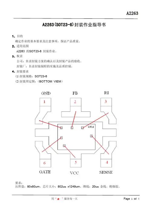
SOT-23-6L PCB封装推荐标准尺寸图
- 格式:pdf
- 大小:198.29 KB
- 文档页数:1
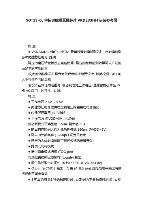
贴片元件封装说明贴片封装 - 两脚表贴现在常用的的电阻、电容、电感、二极管都有贴片封装。
贴片封装用四位数字标识,表明了器件的长度和宽度。
贴片电阻有百分五和百分一两种精度,购买时不特别说明的话就是指百分五。
一般说的贴片电容是片式多层陶瓷电容(MLCC),也称独石电容。
附表是贴片电阻的参数。
英制 (mil) 公制 (mm) 长(L) (mm) 宽(W) (mm) 高(t) (mm) a (mm) b (mm)常规 功率W 提升 功率 W 最大工作 电压 V0201 0603 0.60±0.05 0.30±0.05 0.23±0.05 0.10±0.05 0.15±0.05 1/20 25 0402 1005 1.00±0.10 0.50±0.10 0.30±0.10 0.20±0.10 0.25±0.10 1/16500603 1608 1.60±0.15 0.80±0.15 0.40±0.10 0.30±0.20 0.30±0.20 1/16 1/10 50 0805 2012 2.00±0.20 1.25±0.15 0.50±0.10 0.40±0.20 0.40±0.20 1/10 1/8 150 **** **** 3.20±0.20 1.60±0.15 0.55±0.10 0.50±0.20 0.50±0.20 1/8 1/4 200 1210 3225 3.20±0.20 2.50±0.20 0.55±0.10 0.50±0.20 0.50±0.20 1/4 1/3 200 1812 4832 4.50±0.20 3.20±0.20 0.55±0.10 0.50±0.20 0.50±0.20 1/2 200 2010 5025 5.00±0.20 2.50±0.20 0.55±0.10 0.60±0.20 0.60±0.20 1/2 3/4 2002512 6432 6.40±0.20 3.20±0.20 0.55±0.10 0.60±0.20 0.60±0.20 1200AXIAL - 两脚直插AXIAL 就是普通直插电阻的封装,也用于电感之类的器件。
SOT23-6L单按键触摸耳机芯片VKD233HH封装参考图概述● VKD233DR VinTouchTM 是单按键触摸检测芯片, 此触摸检测芯片内建稳压电路, 提供稳定的电压给触摸感应电路使用, 稳定的触摸检测效果可以广泛的满足不同应用的需求,此触摸检测芯片是专为取代传统按键而设计, 触摸检测PAD 的大小可依不同的灵敏度设计在合理的范围内, 低功耗与宽工作电压, 是此触摸芯片在 DC 或 AC 应用上的特性。
L-03特点● 工作电压 2.4V ~ 5.5V● 内建稳压电路提供稳定的电压给触摸检电路使用● 内建低压重置(LVR)功能● 工作电流 @VDD=3V﹐无负载低功耗模式下典型值 1.5uA、最大值 3uA● 输出响应时间大约为低功耗模式160ms @VDD=3V● 可以由外部电容 (1~50pF) 调整灵敏度● 稳定的人体触摸检测可取代传统的按键开关● 提供低功耗模式● 提供输出模式选择 (TOG pin)可选择直接输出或锁存 (toggle) 输出● 提供最长输出时间约16 秒(±35% @ VDD=3.0V)● Q pin 为CMOS 输出﹐可由 (AHLB pin) 选择高电平输出有效或低电平输出有效● 上电后约有0.5 秒的稳定时间﹐此期间内不要触摸检测点﹐此时所有功能都被禁止● 自动校准功能刚上电的8 秒内约每1 秒刷新一次参考值﹐若在上电后的8 秒内有触摸按键或8 秒后仍未触摸按键,则重新校准周期切换为4 秒应用范围● 各种消费性产品● 取代按钮按键公司的产品涵盖触控、健康量测、工控仪表、航模、小家电、车用及安全监控与智能家居等应用领域,此外还提供各种触摸、LCD/LED驱动、电源管理、MCU及各类控制芯片。
永嘉微电多年来一直坚持聚焦在主航道,抵制一切诱惑;踏踏实实,长期投入,厚积薄发;坚持以客户为主,与客户一起共同创造价值,和客户合作共赢是我们目标。
我们的宗旨是“诚信双赢、品质优秀、客户至上”。
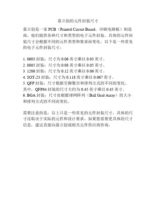
常用元器件封装标准尺寸王永建整理尺寸中的计量单位 mil / 40 = mmDIP 双列封装QFP 四方扁平封装引脚数宽度 mil 引脚数宽度8,14,16,18,20 300 44,48 10*10mm22 400 5214*14mm 24,28,32,40,42,48600 64,80,100,12814*20mm 28,32,40(陶瓷)600 144,160,20828*28mm SKDIP 小双列封装SOP 小外形封装引脚数宽度 mil 引脚数宽度 mil22,24,28,32 300 8,14 15016,14,16,18,20 30028 33032 45044 500SDIP 缩短双列封装SSOP 缩短小型封装引脚数宽度 mil 引脚数宽度 mil40,42,64 600 16,24,28 150 TSSOP 缩短细小型封装20,28 209 引脚数: 8, 20, 48引脚数: 8 MSOP, 48 BQSOP48,56 300NSOP 窄小形双列封装TSOP 细小封装引脚数宽度 mil 引脚数宽度16 150 28,328*13.4mm SOJ 细小封装32 8*14mm 引脚数32 8*20mm28,32QFP 四方扁平封装LQFP 矮四方扁平封装引脚数宽度引脚数宽度44,48 10*10mm 32,44,48 7*7mm52 14*14mm 44,64,80 10*10mm64,80,100,128 14*20mm 80 12*12mm,14*14mm144,160,208 28*28mm 100,128 14*14mm,14*20mm144 20*20mm 208 28*28mmTQFP 细四方扁平封装 其他引脚数宽度类型引脚数 80,100 14*14mmPLCC 塑封大空间封装 SOT-23, SOT-223, SOT-89SOT-25SOT-26 TO-92TO-220, TO-252, TO-26328, 32, 44, 52, 68, 84 3 5 6 3,4 3塑封 DIP/SKDIP/SDIP 尺寸 (单位: mil)SOP/NSOP 封装尺寸(单位: mil)TSSOP 封装尺寸(单位: mil)SOJ 封装尺寸(单位: mil)QFP/LQFP/TQFP 封装尺寸(单位: mil)PLCC 封装尺寸(单位: mil)SOT 23 封装尺寸(单位: mil)SOT 223SOT 89SOT 25SOT 26TO 92TO 220TO 252TO 263 (DD2 PAK)。
嘉立创的元件封装尺寸
嘉立创是一家PCB(Printed Circuit Board,印刷电路板)制造商,他们提供各种尺寸和类型的电子元件封装。
具体的元件封装尺寸会根据不同的元件类型和要求而变化。
以下是一些常见的电子元件封装尺寸:
1. 0603封装:尺寸为0.06英寸乘以0.03英寸。
2. 0805封装:尺寸为0.08英寸乘以0.05英寸。
3. 1206封装:尺寸为0.12英寸乘以0.06英寸。
4. SOT-23封装:尺寸为0.118英寸乘以0.067英寸。
5. QFP封装:尺寸根据引脚数目和排列方式的不同而变化。
其中,QFP64封装的尺寸大约为0.45英寸乘以0.45英寸。
6. BGA封装:尺寸也根据球网阵列(Ball Grid Array)的大小和排列方式的不同而变化。
需要注意的是,以上只是一些常见的元件封装尺寸,具体的尺寸还取决于实际的元件和设计要求。
如果您需要更具体的尺寸信息,建议直接向嘉立创或相关元件供应商咨询。
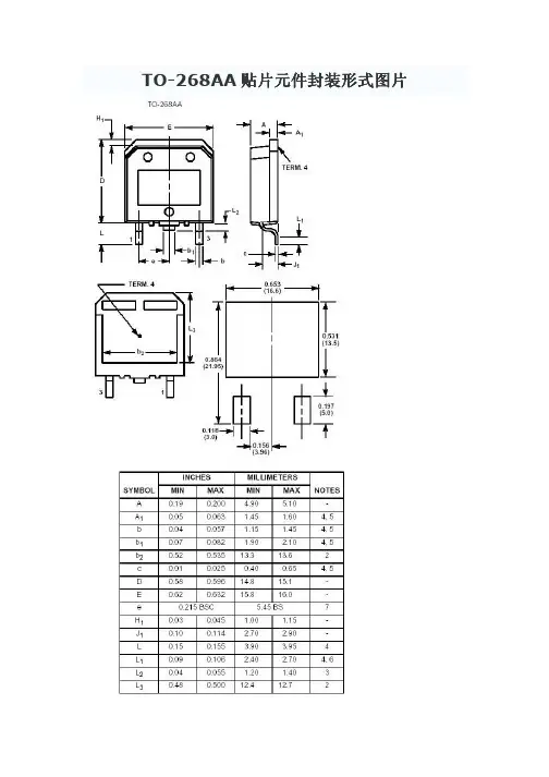
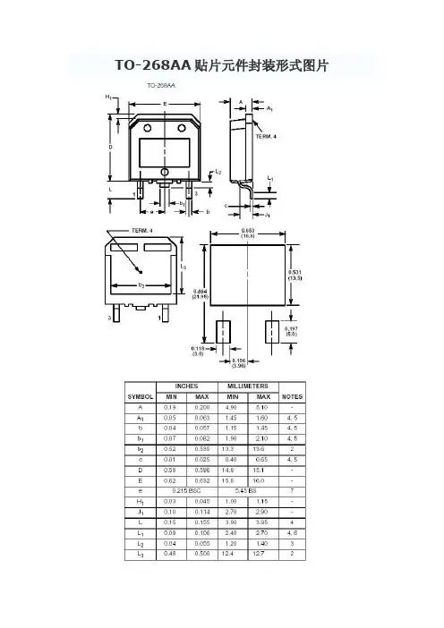
目录TO-268AA贴片元件封装形式图片 (2)TO-263 D2PAK封装尺寸图 (3)TO-263-7封装尺寸图 (4)TO-263-5封装尺寸图 (5)TO-263-3封装尺寸图 (6)TO-252 DPAK封装尺寸图 (7)TO-252-5封装尺寸图 (8)TO252-3封装尺寸图 (9)0201封装尺寸 (10)0402封装尺寸图片 (11)0603封装尺寸图 (12)0805封装尺寸图 (13)01005封装尺寸图 (14)1008封装尺寸图 (15)1206封装尺寸图 (16)1210封装尺寸图 (17)1406封装尺寸图 (18)1812封装尺寸图 (19)1808封装尺寸图 (20)1825封装尺寸图 (21)2010封装尺寸图 (22)2225封装尺寸图 (23)2308封装尺寸图 (24)2512封装尺寸图 (25)DO-215AB封装尺寸图 (26)DO-215AA封装尺寸图 (27)DO-214AC封装尺寸图 (28)DO-214AB封装尺寸图 (29)DO-214AA封装尺寸图 (30)DO-214封装尺寸图 (31)DO-213AB封装尺寸图 (32)DO-213AA封装尺寸图 (33)SOD123H封装图 (34)SOD723封装尺寸图 (35)SOD523封装尺寸图 (36)SOD323封装尺寸图 (37)SOD-123F封装尺寸图 (38)SOD123封装尺寸图 (39)SOD110封装尺寸图 (40)DO-214AC SOD106封装尺寸图 (41)D-7343封装尺寸图 (42)C-6032封装尺寸图 (43)B-3528封装尺寸图 (44)A-3216封装尺寸图 (45)SOT883封装尺寸图 (46)SOT753封装尺寸图 (47)SOT663封装尺寸图 (49)SOT552-1封装尺寸图 (50)1SOT523封装尺寸图 (51)SOT505-1封装尺寸图 (52)SOT490-SC89封装尺寸图 (53)SOT457 SC74封装尺寸图 (54)SOT428封装尺寸图 (55)SOT416/SC75封装尺寸图 (56)SOT663 SMD封装尺寸图 (57)SOT363 SC706L封装尺寸图 (58)SOT353/sc70 5L封装尺寸图 (59)SOT346/SC59封装尺寸图 (60)SOT343 SMD封装尺寸图 (61)SOT323/SC70-3 SMD封装尺寸图 (61)SOT233 SMD封装尺寸图 (62)SOT-223/TO-261AA SMD封装尺寸图 (63)SOT89/TO243AA SC62 SMD封装尺寸图 (64)SOT23-8封装尺寸图 (65)SOT23-5封装尺寸图 (67)SOT23封装尺寸图 (68)SOT143/TO253 SMD封装尺寸图 (69)按住Ctrl键并在目录名上单击鼠标左键,可以跳转到指定页面TO-268AA贴片元件封装形式图片TO-263 D2PAK封装尺寸图TO-252 DPAK封装尺寸图0201封装尺寸0402封装尺寸图片DO-214封装尺寸图SOD123H封装图SOD-123F封装尺寸图DO-214AC SOD106封装尺寸图SOT552-1封装尺寸图。
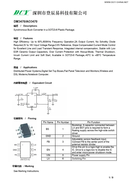
DM3470/AO3470Synchronous Buck Converter in a SOT23-6 Plastic Package.High Efficiency: Up to 93%,600KHz Frequency Operation,2A Output Current, No Schottky Diode Required,3V to 18V Input Voltage Range,0.6V Reference, Slope Compensated Current Mode Control for Excellent Line and Load Transient Response, Integrated internal compensation, Stable with Low ESR Ceramic Output Capacitors, Over Current Protection with Hiccup-Mode, Thermal Shutdown, Inrush Current Limit and Soft Start, Available in SOT23-6 Package,-40°C to +85°C Temperature Range.Distributed Power Systems,Digital Set Top Boxes,Flat Panel Television and Monitors,Wireless and DSL Modems,Notebook Computer.印章代码 / Marking描述 / Descriptions特征 / Features用途 / Applications内部等效电路 / Equivalent Circuit引脚排列 / PinningPin NamePin NumberPin FunctionBS 1Bootstrap. A capacitor connected between LX and BST pins is required to form afloating supply across the high-side switch driver.GND 2 GroundFB 3 Adjustable version feedback input.Connect FB to the center point of theexternal resistor divider.EN 4 Drive this pin to a logic-high to enable theIC. Drive to a logic-low to disable the ICand enter micro-power shutdown mode.VIN 5 Power supply Pin LX 6 Switching Pin132 45 6参数Parameter符号 Symbol 数值 Rating 单位 Unit Vin Voltage V DD -0.3 to 20 V LX Voltage V M -0.3 to (Vin+0.5V)V EN Voltage V CO -0.3 to 20 V FB Voltage V DO -0.3 to 6 V BS VoltageT opr-0.3 to (VLX+5V)VJunction Temperature T stg 150 °C Operating Temperature-40°C to +85°C参数Parameter符号 Symbol测试条件 Test Conditions最小值Min 典型值Typ 最大值Max单位Unit Input Voltage Range V DD 4.516VUVLO ThresholdC O3.0 V Supply Current in Operation V st VEN=2.0V, VFB=1.1V 0.4 0.6 mA Supply Current in Shutdown R short VEN =0 or EN = GND 1uA Regulated Feedback Voltage T A = 25°C, 4.5V ≤VIN ≤18V 0.5880.6 0.612V High-Side Switch On-Resistance 90 m Ω Low-Side Switch On-Resistance70m ΩHigh-Side Switch Leakage CurrentVEN =0V, VLX =0V 0 10 uA Upper Switch Current Limit I DD Minimum Duty Cycle3AOscillation Frequency I st1 0.6 MHz Maximum Duty Cycle VFB=0.6V 92 % Minimum On-Time 60 nS Thermal Shutdown160℃极限参数 / Absolute Maximum Ratings(Ta=25℃) 电性能参数 / Electrical Characteristics(Ta=25℃) DM3470/AO3470The DM3470 is a current mode st Internal Regulatorep down DC/DC converter that provides excellent transient response with no extra external compensation components. This device contains an internal, low resistance, high voltage power MOSFET, and operates at a high 600K operating frequency to ensure a compact, high efficiency design with excellent AC and DC performance.Error AmplifierThe error amplifier compares the FB pin voltage with the internal FB reference (VFB) and outputs a current proportional to the difference between the two. This output current is then used to charge or discharge the internal compensation network to form the COMP voltage, which is used to control the power MOSFET current. The optimized internal compensation network minimizes the external component counts and simplifies the control loop design.Internal Soft-StartThe soft-start is implemented to prevent the converter output voltage from overshooting during startup. When the chip starts, the internal circuitry generates a soft-start voltage (SS) ramping up from 0V to 0.6V. When it is lower than the internal reference (REF), SS overrides REF so the error amplifier uses SS as the reference. When SS is higher than REF, REF regains control. The SS time is internally fixed to 1 ms.Startup and ShutdownIf both VIN and EN are higher than their appropriate thresholds, the chip starts. The reference block starts first, generating stable reference voltage and currents, and then the internal regulator is enabled. The regulator provides stable supply for the remaining circuitries. Three events can shut down the chip: EN low, VIN low and thermal shutdown. In the shutdown procedure, the signaling path is first blocked to avoid any fault triggering. The COMP voltage and the internal supply rail are then pulled down. The floating driver is not subject to this shutdown command.Setting the Output VoltageThe external resistor divider is used to set the output voltage (see Typical Application on page 1). The feedback resistor R1 also sets the feedback loop bandwidth with the internal compensation capacitor. Choose R1 to be around 100k Ω for optimal transient response. R2 is then given by:1/12−=FB out V V R RSelecting the InductorA 4.7μH to 22μH inductor with a DC current rating of at least 25% percent higher than the maximum load current is recommended for most applications. For highest efficiency, the inductor DC resistance should be less than 15m Ω. For most designs, the inductance value can be derived from the following equation.OSC L in out in out f I V V V V L ×Δ×−×=)(Where ΔIL is the inductor ripple current. Choose inductor ripple current to be approximately 30% if the maximum load current, 2A. The maximum inductor peak current is:2)(LLOAD MAX L I I I Δ+=Under light load conditions below 100mA, larger inductance is recommended for improved efficiency.Selecting the Output CapacitorThe output capacitor (C2) is required to maintain the DC output voltage. Ceramic, tantalum, or low ESR electrolytic capacitors are recommended. Low ESR capacitors are preferred to keep the output voltage ripple low. The output voltage ripple can be BRCDmated by:⎥⎦⎤⎢⎣⎡××+×⎥⎦⎤⎢⎣⎡−××=Δ2811C f R V V L f V V S ESR IN OUT S OUT OUTcan be DMmated by:The characteriDCY cs of the output capacitor also af DM3470 can be optimized for a wide range of capacitance and ESR values. Where L is the inductor value and RESR is the equivalent series resistance (ESR) value of the output capacitor. In the case of ceramic capacitors, the impedance at the switching frequency is dominated by the capacitance. The output voltage ripple is mainly caused by the capacitance. For simplification,the output voltage ripple ⎥⎦⎤⎢⎣⎡−××××=ΔIN OUT S OUTOUTV V C L f V V 1822In the case of tantalum or electrolytic capacitors, the ESR dominates the impedance at the switching frequency. For simplification, the output ripple can be approximated to:ESR IN OUT S OUT OUT R V V L f V V ×⎥⎦⎤⎢⎣⎡−××=Δ1fect the stability of the regulation system. ThePCB Layout GuidePCB layout is very important to achieve stable operation. It is highly recommended to duplicate EVB layout for optimum performance. If change is necessary,please follow these guidelines and take Figure 4 for reference.1) Keep the path of switching current short and minimize the loop area formed by Input capacitor, high-side MOSFET and low-side MOSFET.2) Bypass ceramic capacitors are suggested to be put close to the Vin Pin.3) Ensure all feedback connections are short and direct. Place the feedback resistors and compensation components as close to the chip as possible. 4) VOUT, LX away from sensitive analog areas such as FB.5) Connect IN, LX, and especially GND respectively to a large copper area to cool the chip to improve thermal performance and long-term reliability.结构图/ Block Diagram:外形尺寸图 / Package DimensionsDM3470/AO3470印章说明 / Marking Instructions说明: 3470:为型号代码****:为生产批号代码,随生产批号变化。
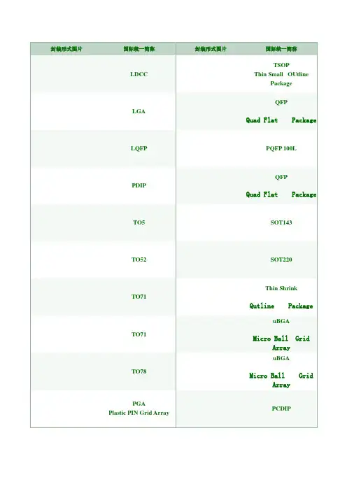
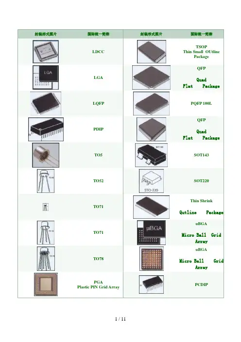
封装形式图片国际统一简称LDCCLGALQFPPDIPTO5TO52TO71TO71TO78PGAPlastic PIN Grid Array 封装形式图片国际统一简称TSOPThin Small OUtlinePackageQFPQuad Flat PackagePQFP 100LQFPQuad Flat PackageSOT143SOT220Thin ShrinkQutline PackageuBGAMicro Ball GridArrayuBGAMicro Ball GridArrayPCDIPPLCCLQFPLQFP 100LTO8TO92TO93T099EBGA 680LQFPQuad Flat PackageTQFP 100LZIPZig-Zag Inline PackaSOT223SOT223SOT23SOT23/SOT323SOT25/SOT353SOT26/SOT363FBGAFDIPSOJSBGALBGA 160LPBGA 217LPlastic Ball GridArraySBGA 192LTSBGA 680LCLCCSC-705LSDIPSIPSingleInline PackageSOSmall OutlinePackageSOP EIAJ TYPE II 14LSSOP 16LSSOPSOJ 32LFlat PackHSOP28ITO220ITO3PTO220TO247CNRCPGACeramic Pin OutlinePackageDIPDualInline PackageDIP-tabDUAL Inline Package with Metal HeatsinkBQFP 132C-BendLeadCERQUAD Ceramic Quad FlatCeramicCase LAMINATE CSP T12L Chip Scale PackageGullwingleadsTO264TO3JLCCLCCTO263/TO268SO DIMMSmall Outline Dual In-line Memory ModuleSOCKET 370For intel 370 Pin PGA PentiumIII & CeleronCPUSIMM30Single Inline MemoryModuleSIMM72Single Inline MemoryModuleSIMM72Single inline MemoryModuleSOT343SOT523SOT89SOT89Socket 603FosterLLP 8LaPCI 32bit 5V Peripheral Component InterconnectPCI 64bit 3.3V Peripheral Component InterconnectPCMCIATCSP 20LChip Scale Packagepin PGApentium 4 CPUSOCKET462/SOCKET A For PGA AMD Athlo & Duron CPUPSDIPSLOT1 For intel pentiumII petiumIII &Celeron CPUSLOT A For AMDAthloncpuSNAPTKSNAPTKSNAPZPSOHBGABall Grid Array一、直插式电阻封装及尺寸直插式电阻封装为AXIAL-xx形式(比如AXIAL-0.3、AXIAL-0.4),后面的xx 代表焊盘中心间距为xx英寸,这一点在网上很多文章都没说清楚,单位为英寸。