高速数据采集系统设计
- 格式:doc
- 大小:356.00 KB
- 文档页数:12
高速数据采集与处理系统设计研究随着科技的不断进步和社会的快速发展,数据已经成为了企业决策和业务开展的最重要资源之一。
为了更好地收集和处理数据,不少企业开始采用高速数据采集与处理系统。
本文将详细介绍高速数据采集与处理系统的设计研究,重点探讨其应用场景、数据处理流程和技术实现。
一、高速数据采集与处理系统的应用场景高速数据采集与处理系统适用于数据量极大、实时性要求高的企业。
比如金融行业的交易数据、电信运营商的通信数据、物流公司的运输数据等等。
在这些场景下,数据的产生和流动速度非常快,传统的数据采集和处理方案已经无法胜任。
二、高速数据采集与处理系统的数据处理流程高速数据采集与处理系统的数据处理流程相对于传统的数据处理方案来说更加简单高效。
常用的数据处理流程包括以下几个步骤:1. 数据采集:通过网络、传感器等方式对产生的数据进行采集。
2. 数据传输:将采集到的数据通过网络传输至数据中心。
3. 数据处理:对采集到的数据进行处理,包括数据清洗、数据分析、数据挖掘等等。
4. 数据存储:将处理后的数据存储到数据库中,以便于后续的数据分析和业务决策。
5. 数据展示:通过数据可视化工具将处理后的数据以图表等形式进行展示。
三、高速数据采集与处理系统的技术实现高速数据采集与处理系统的技术实现主要依赖于以下几个方面:1. 异步模型:通过异步模型实现高并发的数据采集和处理。
2. 分布式计算:将数据处理的任务分散到多台服务器上进行并行计算,提高数据处理效率。
3. 大数据存储:通过大数据存储技术,可以高效地存储处理后的数据。
4. 数据可视化:通过数据可视化工具可视化处理后的数据,便于用户进行数据分析和业务决策。
四、高速数据采集与处理系统的优势相比传统的数据采集和处理方案,高速数据采集与处理系统具有以下几个优势:1. 高效性:高速数据采集与处理系统可以实现实时数据采集,对数据进行高效的处理和存储。
2. 稳定性:高速数据采集与处理系统可靠性高,能够在高并发的情况下正常运行。
基于FPGA的高速数据采集系统设计与实现的开题报告一、选题背景与意义在现代工业领域,高速数据采集是必不可少的环节,对于某些应用场景,如医学图像、通信信号和自然界信号的采集等,必须保证采样率高、抗噪性强的特点。
面对如此巨大的数据采集挑战,传统基于PC机的采集系统已经难以满足实时性和高速性的要求,而基于FPGA的高速数据采集系统从其高速、高精度、低功耗、灵活可靠等诸多特点上来看,成为了实现高速数据采集的首选方案。
因此,本文将对基于FPGA的高速数据采集系统设计与实现开题进行研究。
二、研究内容本课题旨在通过对基于FPGA的高速数据采集系统设计与实现开题进行深入研究,侧重于以下几个方面:1. 基于FPGA芯片架构的深入研究,尤其是在高速、可靠、低功耗等方面的性能表现。
2. 研究采样率、信噪比、滤波器等方面在数据采集系统中的应用。
3. 设计高速数据采集控制系统,探究其在高速数据采集系统中的作用和设计原理。
4. 进行基于FPGA的高速数据采集系统硬件电路设计、软件编码及实现,并通过实验验证其性能。
三、研究方法本文采用计算机仿真分析和实验研究相结合的方法,首先通过软件工具对系统进行模拟,了解系统设计的基本原理和方法,然后进行硬件电路设计和软件编码,实现实际的高速数据采集系统,最后对实验结果进行分析和总结。
四、预期成果1. 实现一套基于FPGA的高速数据采集系统,该系统具有高速性、稳定性、可靠性、低功耗等优点。
2. 对该系统进行了性能测试,并分析系统在数据采集过程中的表现及优劣。
3. 从系统设计、电路设计、软件编写三个角度,对基于FPGA的高速数据采集系统设计与实现开题进行了研究,并提出了可供参考的经验和具体指导意见。
五、可能面临的问题及解决方案1. FPGA硬件电路设计难度大。
解决方案:参考多数学者的研究成果,针对不同应用,找出符合实际需要的电路设计。
2. 信号处理算法的开发。
解决方案:充分利用智能算法,设计高效低延迟的算法并进行实际验证。
基于FPGA的高速数据采集系统设计随着科学技术的不断进步,数据采集系统在许多领域都发挥着重要作用。
为了满足高速数据采集的需求,基于现场可编程门阵列(FPGA)的高速数据采集系统设计应运而生。
本文将介绍这一系统的设计原理和关键技术。
首先,我们需要了解FPGA的基本原理。
FPGA是一种可编程的硬件设备,可以根据需要重新配置其内部逻辑电路。
这使得FPGA在数据采集系统中具有极大的灵活性和可扩展性。
与传统的数据采集系统相比,基于FPGA的系统可以实现更高的采样率和更低的延迟。
基于FPGA的高速数据采集系统设计主要包括以下几个关键技术。
首先是模数转换(ADC)技术。
ADC是将连续的模拟信号转换为数字信号的关键环节。
在高速数据采集系统中,需要使用高速、高精度的ADC来保证数据的准确性和完整性。
其次是FPGA内部逻辑电路的设计。
为了实现高速数据采集,需要设计高效的数据处理逻辑电路。
这些电路可以实现数据的实时处理、存储和传输等功能。
同时,还需要考虑电路的时序约束和资源分配等问题,以确保系统的稳定性和可靠性。
另外,时钟同步技术也是高速数据采集系统设计的重要内容。
在高速数据采集过程中,各个模块需要保持同步,以确保数据的准确性。
因此,需要设计合理的时钟同步方案,保证各个模块在同一个时钟周期内完成数据的采样和处理。
最后,还需要考虑系统的接口和通信问题。
基于FPGA的高速数据采集系统通常需要与其他设备进行数据交互,如计算机、存储设备等。
因此,需要设计合适的接口和通信协议,实现数据的传输和存储。
综上所述,基于FPGA的高速数据采集系统设计涉及多个关键技术,包括ADC技术、FPGA内部逻辑电路设计、时钟同步技术以及接口和通信问题。
通过合理的设计和优化,可以实现高速、高精度的数据采集,满足现代科学研究和工程应用的需求。
这将为各个领域的数据采集工作带来巨大的便利和发展空间。
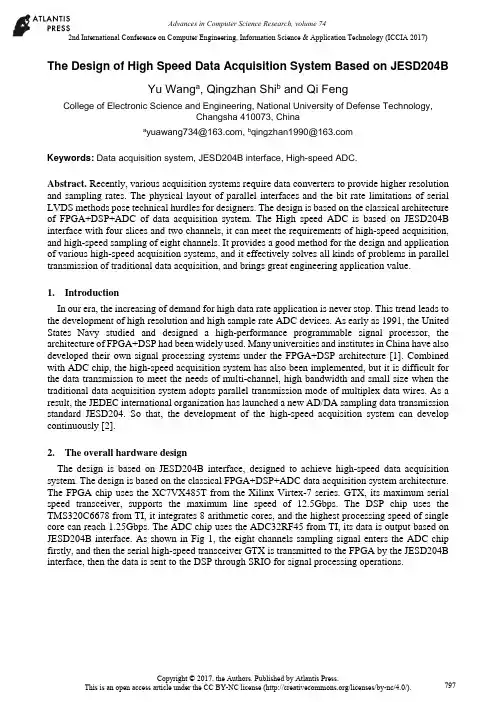
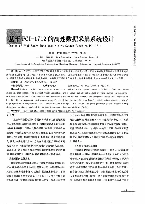
2nd International Conference on Computer Engineering, Information Science & Application Technology (ICCIA 2017)The Design of High Speed Data Acquisition System Based on JESD204BYu Wang a, Qingzhan Shi b and Qi FengCollege of Electronic Science and Engineering, National University of Defense Technology,Changsha 410073, Chinaa******************,b********************Keywords: Data acquisition system, JESD204B interface, High-speed ADC.Abstract. Recently, various acquisition systems require data converters to provide higher resolution and sampling rates. The physical layout of parallel interfaces and the bit rate limitations of serial LVDS methods pose technical hurdles for designers. The design is based on the classical architecture of FPGA+DSP+ADC of data acquisition system. The High speed ADC is based on JESD204B interface with four slices and two channels, it can meet the requirements of high-speed acquisition, and high-speed sampling of eight channels. It provides a good method for the design and application of various high-speed acquisition systems, and it effectively solves all kinds of problems in parallel transmission of traditional data acquisition, and brings great engineering application value.1.IntroductionIn our era, the increasing of demand for high data rate application is never stop. This trend leads to the development of high resolution and high sample rate ADC devices. As early as 1991, the United States Navy studied and designed a high-performance programmable signal processor, the architecture of FPGA+DSP had been widely used. Many universities and institutes in China have also developed their own signal processing systems under the FPGA+DSP architecture [1]. Combined with ADC chip, the high-speed acquisition system has also been implemented, but it is difficult for the data transmission to meet the needs of multi-channel, high bandwidth and small size when the traditional data acquisition system adopts parallel transmission mode of multiplex data wires. As a result, the JEDEC international organization has launched a new AD/DA sampling data transmission standard JESD204. So that, the development of the high-speed acquisition system can develop continuously [2].2.The overall hardware designThe design is based on JESD204B interface, designed to achieve high-speed data acquisition system. The design is based on the classical FPGA+DSP+ADC data acquisition system architecture. The FPGA chip uses the XC7VX485T from the Xilinx Virtex-7 series. GTX, its maximum serial speed transceiver, supports the maximum line speed of 12.5Gbps. The DSP chip uses the TMS320C6678 from TI, it integrates 8 arithmetic cores, and the highest processing speed of single core can reach 1.25Gbps. The ADC chip uses the ADC32RF45 from TI, its data is output based on JESD204B interface. As shown in Fig 1, the eight channels sampling signal enters the ADC chip firstly, and then the serial high-speed transceiver GTX is transmitted to the FPGA by the JESD204B interface, then the data is sent to the DSP through SRIO for signal processing operations.FPGA DSPADC x4SRIO PCIEGPIOJESD204B 8Channel FLASH DDR3x4GbpsEthernet FLASH DDR3x2HDMIFig.1 System overall structure diagramIn the design of the data acquisition system, the FPGA’s external interface HDMI, a 19 pin high-speed data interface, is used for data’s communication with external memory. On the board, we connect the four differential signal line of the FPGA’s high speed serial transceiver (GTX) to the HDMI interface. The external high-speed interface of DSP adopts Gigabit Ethernet to realize high-speed data transmission. Both the FPGA and the DSP have an external 256MB Flash memory, In addition, the FPGA has two DDR3 external memory to form the storage space of the 1GB, DSP has four DDR3 memory external to form the storage space of 2GB.3. JESD204B InterfaceIn the field of PC and embedded systems, it has been an empty talk that the method for improving bus bandwidth by raising bus operating frequency under the condition of a parallel bus data width. It cannot be realized at all because of the influence of technology and environment in the actual implementation. Therefore, the communication structure of the serial bus is changed from parallel bus communication. Typically, the ADC is 12~16 bit data lines, and strictly required to be aligned on one edge of the clock. The higher frequency the ADC operating, the greater data offset between the data lines, and then synchronization between data is becoming more difficult. The JEDEC international organizations have fully learned the advantages of PCIE/SRIO and other serial bus communication protocols based on data packet (frame format). The JESD204 protocol was introduced in 2006, it is the a differential pair adopted the CML level, instead of the 12~16 bit parallel data line, realizing serial communication interface and supporting the highest 3.125Gbps data transmission rate of ADC device. In January 2012, the JESD204 bus protocol has been upgraded to the JESD204 B.01 version, the maximum transmission rate of each pair of differential lines is supported by 12.5Gbps [3,4]. Table 1 Comparison of JESD204 with other interfacesNumber of Channels Resolution CMOS Pin Count LVDS Pins Count (DDR) CML Pin Count (JESD204B)1 14 13 14 42 14 26 28 44 14 52 56 68 14 104 112 6Fig.2 CMOS, LVDS, and CML Driver Power ComparisonIn summary, the advantages of JESD204B include the following three points:(1) Decreased in pin number, simplified system design, greatly simplified the wiring between ADC and FPGA(2) Because wiring is simpler and pin number is less, using JESD204B will make the package smaller and simpler.(3) High speed ADC devices consume less power per unit after adopting CML level.At present, the TI, the ADI and other companies have their latest high-speed ADC chip based on the JESD204B interface. ADC32RF45 released by TI, AD9625 released by ADI, and the latest AD9208 released by ADI Company in April 2017, these all belong to the new ADC series adopted with JESD204B interface. In respect of Field Programmable logic device (FPGA), the company, such as Xilinx and Altera, also supports the JESD204B interface. In addition there are JESD204B dedicated clock chip, such as LMK042828, HMC7044 and so on.4.The Key of ADC design interfaceWe can implement the JESD204B protocol by FPGA's GTX interface, to parse the data emitted by ADC correctly. The hardware uses the FPGA’s GTX interface directly, and the GTX is connected with the data-in pin of the ADC. ADC data-out pin as the sending end, FPGA GTX port as the receiving end, to achieve data transmission on the line [5]. The software uses the 8B/10B codec module and the control character detection module which are embedded in the GTX interface.low two bit make up a frame with 16bit data. After framing, the data is encoded by 8B/10B, then it becomes 20 bit. Sending to Serial high-speed transceiver GTX of FPGA, FPGA complete the operation of the 8B/10B decoding and the analysis of JESD204B protocol. Setting the ADC32RF45 sample clock to 2.5GHz, the rate corresponding to the encoding at all levels is shown below.Table 2 Comparison of JESD204BClock/GH z Data-width/bit Rate/Gbp sRemark Original data 2.5 14 8.4 ADC Sampled DataFraming 2.5 16 10 Zero-paddingCoding 2.5 20 12.5 8B/10BThe ADC is dual channel, each channels has 4 lanes, that is, 4 pairs of CML data lines. As can be seen from the chart above, ADC eventually sends the sampled data at a rate of 12.5Gbps, GTX, the receiving rate of the FPGA side should also be set to 12.5Gbps.5. Clock designJESD204B begins with the edge of the clock signal to identify synchronization. And through a certain handshake signal, the sender and receiver can correctly recognize the frame length and boundaries. Therefore, the clock signal and its timing relation are extremely important to JESD204B. The following is a multi-device synchronization solution for the JESD204B system, the Device Clock is the main clock for the device operation. A clock that is usually sampled in a digital to analog converter or a clock with integer multiples. The frame and multi frame clock of the protocol itself are also based on Device Clock. SYSREF is the edge of the Device Clock used to indicate different converters or logic, or the reference delay between different devices.In the JESD204B system, the synchronization of data converters can be broken down into four basic requirements. These requirements are vividly depicted in Fig.4.(1) The phase alignment of the device clock is implemented on each data converter;(2) The setting and holding time of the SYSREF (relative to the device clock) are met on each data converter and logic element;(3) An appropriate resilient buffer release point is selected in the JESD204B receiver to ensure deterministic delay; (4) Need to meet the SYNC signal timing requirements when necessary. A D CA D CA D CA D C Data SYNC DataSYNC Data SYNCDevice Clock SYSREF Device ClockSYSREF Device Clock SYSREFDevice ClockSYSREFLogic DeviceClock Distirbution DataSYNCFig.4 Multi device synchronization solution for JESD204B systemADI and TI have high performance clock jitter attenuator with JESD204B, such as HMC7044, LMK04828 and so on. Their Device Clock, and SYSREF are paired output, its output timing meets its timing requirements, and its application is relatively simple.6.ConclusionThis paper utilizes the advanced high-speed ADC with JESD204B interface, combine the latest ADC chip and Xilinx 7 Series resources, and proposes the design of high-speed data acquisition system based on JESD204B. This paper first describes the overall design of the system, and then we detailed for each module design. We first solve the core processing module of FPGA+DSP. Both of FPGA and DSP communicate with each other through SRIO, FPGA pretreatment data is sent to the DSP for signal processing. Utilizing existing technology and hardware, a high-speed data acquisition system is designed with the JESD204B interface ADC which has higher resolution and higher sampling rate (3Gbps or so). It can be well suited to eight channel high-speed sampling, the design is miniaturized and the wiring is simpler. FPGA resource consumption is reduced by about half of resources compared to traditional parallel data lines, it has great prospect of engineering application. References[1] Ran Yan, XI Pengfei. High Speed Serial Data Acquisition System Based on JESD204 Protocol [J].Electronic Sci. & Tech. 2015, 28(5):17-19[2] Zhou Yuxuan, Clock Circuit Design of 2.5 GSPS High Resolution Data Acquisition System [D].UESTC, 2016[3] ADI. JESD204B Survival Guide [M]. [USA]: ADI, 2013[4] ADI. JESD204B serial interface clock requirements and their implementation [M]. [USA]: ADI,2013[5] Xilinx. 7 Series FPGAs GTX/GTH Transceivers [M]. USA: Xilinx, 2016.。
高速公路交通信息采集系统设计随着社会经济的快速发展和人们生活水平的不断提高,交通问题逐渐成为制约国家发展的重要因素之一。
在现代城市中,交通拥堵已经成为了人们生活中的一大烦恼,而高速公路交通信息采集系统的设计,就是为了解决这个问题。
本文将从设计的背景、设计的目标和设计的方案等方面,对高速公路交通信息采集系统进行探讨。
一、设计的背景随着城市化进程的加速,人口的大规模流动和车辆的快速增加,交通拥堵的问题越来越严重。
高速公路作为重要的交通设施,承载着大量的车流和人流,但是由于车辆数量的增加,导致高速公路的交通流量越来越大,交通拥堵问题日益严重。
同时,传统的高速公路交通管理方法已经不能很好地处理复杂的交通环境,迫切需要一种新的高效交通信息处理系统来更好地管理高速公路交通。
二、设计的目标高速公路交通信息采集系统的设计的目标,是帮助交通管理部门更好地处理交通信息,实现道路交通的科学管理。
具体地说,它可以实现以下几个方面的目标:1. 实现高速公路实时监控。
利用高精度跟踪技术,通过自动化的摄像头系统,实现对道路上的行车情况进行实时监测,为交通管理者提供实时的路况数据。
2. 提高交通安全水平。
通过对道路上的交通信息进行采集和处理,及时发现各种交通违规行为,并及时进行处理,提高交通规范度和安全水平。
3. 降低耗时和物力成本。
通过智能化的高速公路交通信息采集系统,自动化的完成各种交通信息的收集和处理,降低人力资源和物资投入成本,提高道路交通的效率。
4. 实现路况预测功能。
通过对历史数据和实时采集的数据进行分析,对未来的交通情况进行预测。
为交通部门提供预测数据,帮助其更好地制定管理决策。
三、设计方案高速公路交通信息采集系统的设计中,需要解决以下几个重点问题:1. 数据采集和处理高速公路交通信息的采集和处理,是系统设计的核心和难点。
通过高精度的摄像头和相关传感器,对道路上的车辆行驶情况进行实时监测,并通过智能化算法对各种信息(如车辆数量、速度、车型、车牌等)进行采集和处理,通过智能分析技术和大数据处理技术,对采集的数据进行分析和处理,生成管理人员所需要的各类报表和图表,达到及时监管和迅速反应的目的。
目录1.绪论 (1)1.1 课题研究的意义 (1)1.2 数据采集技术的发展历程和现状 (1)1.3 本文的研究内容 (2)1。
4 系统设计涉及的理论分析 (2)2.系统设计 (4)2.1方案选择 (4)2。
2系统框图 (5)3.单元电路设计 (6)3.1信号调理电路 (6)3.2高速A/D模块 (7)3。
3 FPGA模块设计 (8)3。
4MCU模块设计 (8)3.5数据采集通道总体原理图 (9)3.6硬件电路总体设计 (9)4。
软件设计 (10)4。
1 信号采集与存储控制电路工作原理 (10)4.2 信号采集与存储控制电路的FPGA实现 (11)4.3 原理图中的各底层模块采用VHDL语言编写 (12)4。
3。
1三态缓冲器模块TS8 (12)4.3。
2分频器模块fredivid (13)4.3.3地址锁存器模块dlatch8 (14)4。
3.4地址计数器模块addrcount (15)4.3.5双口RAM模块lpm_ram_dp (16)4.4 数据显示模块设计 (18)4。
4.1 主程序 (18)4。
4。
2 INT0中断服务程序 (19)4。
4.3 INT1中断服务程序 (19)4。
5软件仿真 (20)4.5.1三态缓冲器模块TS8 (20)4。
5.2分频器模块fredivid (20)4。
5。
3地址锁存器模块dlatch8 (20)4.5。
4地址计数器模块addrcount (21)5。
系统调试 (21)5.1 单片机子系统调试 (21)5。
2 FPGA子系统调试 (22)5.3 高速A/D模块的调试 (22)6 总结 (22)致谢 (22)参考文献 (23)附录 (25)高速数据采集系统设计摘要:随着数字技术的飞速发展,高速数据采集系统也迅速地得到了广泛的应用.在生产过程中,应用这一系统可以对生产现场的工艺参数进行采集、监视和记录,为提高生产质量,降低成本提供了信息和手段。
在科学研究中,应用数据采集系统可以获取大量的动态数据,是研究瞬间物理过程的有力工具,为科学活动提供了重要的手段.而当前我国对高速数据采集系统的研究开发都处于起步阶段,因此,开发出高速数据采集系统就显得尤为重要了。
高速数据采集系统设计的关键技术研究在当今信息爆炸的时代,数据采集系统扮演着至关重要的角色,尤其是对于需要处理大量实时数据的任务来说,高速数据采集系统是必不可少的。
设计一个高速数据采集系统涉及到许多关键技术,本文将就这些技术进行探讨和研究。
首先,高速数据采集系统设计中的一个关键技术是数据传输技术。
在处理大量实时数据的情况下,数据传输的速度和稳定性是至关重要的。
采用高效率的数据传输协议,如TCP/IP、UDP等,可以有效提高数据传输的效率和稳定性。
此外,采用多线程技术和异步数据传输方式,可以进一步提高数据传输的速度和效率。
其次,高速数据采集系统设计中的另一个关键技术是数据存储技术。
对于大量实时数据的处理,一个高效的数据存储系统是必不可少的。
采用高性能的数据库系统,如MongoDB、Redis等,可以有效提高数据的存储和查询速度。
此外,采用数据压缩和索引技术,可以进一步提高数据存储的效率和节约存储空间。
除此之外,在高速数据采集系统设计中,还需要考虑到数据清洗、数据转换和数据质量控制等关键技术。
数据清洗是指对原始数据进行去重、去噪、修复等处理,以提高数据的准确性和完整性。
数据转换是指将不同格式、不同结构的数据进行转换和整合,以便于后续分析和处理。
数据质量控制是指对采集到的数据进行监控和评估,确保数据的质量和可靠性。
总的来说,高速数据采集系统的设计涉及到多个关键技术,包括数据传输技术、数据存储技术、数据清洗技术、数据转换技术和数据质量控制技术等。
只有在这些关键技术上做到充分的研究和优化,才能设计出高效稳定的高速数据采集系统,满足实时数据处理的需求。
希望通过对这些关键技术的研究和应用,可以进一步推动高速数据采集系统的发展和应用。
高速数据采集与实时处理系统的设计与实现随着科技不断发展,数据在我们生活中的地位越来越重要。
特别是在工业自动化领域中,高速数据采集和实时处理系统的需求越来越大。
本文将介绍高速数据采集与实时处理系统的设计与实现。
本文主要包括以下几个方面:1. 高速数据采集系统的设计与实现2. 实时数据处理系统的设计与实现3. 系统的测试和性能优化1. 高速数据采集系统的设计与实现高速数据采集是指突破常用采集速度,进行数据采集和传输的一种技术。
在工业自动化控制中,电子元器件的响应速度非常快,因此需要实时采集数据才能更好地对工控设备进行控制和实现数据分析。
以下是高速数据采集系统的设计和实现步骤:1.1 选型硬件和软件首先需要选定采集设备和软件。
在选定硬件时需考虑采集速度、采集量、输入接口以及多通道采集等因素。
对于实时控制系统,应选用高速、稳定且可靠的硬件设备。
软件方面,根据硬件的选择,选用适当的驱动程序。
1.2 电路设计由于需要保证采集器的稳定性和可靠性,因此电路设计十分重要。
在设计电路时,需要特别注意信号放大放大电路的设计和噪声干扰的屏蔽。
在信号传输过程中,信号放大电路应具有高增益,同时应能有效地屏蔽来自外部线路的噪声干扰。
1.3 布线设计由于布线和绝缘的设计将直接影响采集数据的稳定性和准确性,因此需要采用专业的设计技术和规范,确保系统数据的稳定。
1.4 系统调试系统调试是整个设计过程中最重要的环节之一。
在进行系统调试时,应逐一对硬件设备和软件进行测试和校准。
检查系统的分辨率是否满足要求,数据采集是否准确和稳定,软件编程是否准确等等。
只有经过严格的测试和校准,才能确保实时数据采集的准确性和稳定性。
2. 实时数据处理系统的设计与实现2.1 数据处理系统的选择在设计实时数据处理系统时,选择合适的数据处理系统非常重要。
根据实际需要,选择处理器和软件。
处理器的性能要足够强大,以处理高速实时数据。
软件也要适应处理器,为系统提供有效、快速和准确的数据处理。
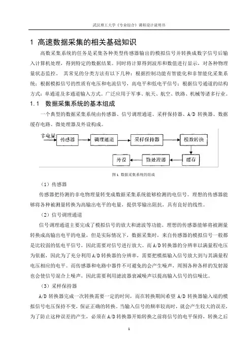
1 高速数据采集的相关基础知识高数采集系统的任务是采集各种类型传感器输出的模拟信号并转换成数字信号后输入计算机处理,得到特定的数据结果。
同时将计算得到波形和数值进行显示,对各种物理量状态监控。
其常见的分类方法有以下几种:根据控制功能有智能化和非智能化采集系统;根据模拟信号的性质有电压和电流信号,高电平和低电平信号;根据信号通道的结构方式:单通道及多通道输入方式。
广泛应用于军事、航天、航空、铁路、机械等诸多行业。
1.1数据采集系统的基本组成一个典型的数据采集系统由传感器、信号调理通道、采样保持器、A/D转换器、数据缓存电路、微处理器及外设构成。
图1 数据采集系统的组成(1)传感器传感器把待测的非电物理量转变成数据采集系统能够检测的电信号。
理想的传感器能够将各种被测量转换为高输出电平的电量,提供零输出阻抗,具有良好的线性。
(2)信号调理通道信号调理通道主要完成了模拟信号的放大和滤波等功能。
理想的传感器能够将被测量转换成高输出电平的电量,但是实际情况下,数据采集时,来自传感器的模拟信号一般都是比较弱的低电平信号,因此需要对信号进行放大。
而A/D转换器的分辨率以满量程电压为依据,因此为了充分利用A/D转换器的分辨率,需要把模拟输入信号放大到与其满量程电压相应的电平。
而传感器和电路中器件不可避免的会产生噪声,周围各种各样的发射源也会使信号混合上噪声,因此需要利用滤波器衰减噪声以提高输入信号的信噪比。
(3)采样保持器A/D转换器完成一次转换需要一定的时间,而在转换期间希望A/D转换器输入端的模拟信号电压保持不变,保证正确的转换。
当输入信号的频率较高时,就会产生较大的误差,为了防止这种误差的产生,必须在A/D转换器开始转换之前将信号的电平保持,转换之后又能跟踪输入信号的变化,保证较高的转换精度。
为此,需要利用采样保持器来实现。
(4)A/D转换器模拟信号转换成数字信号之后,才能利用微处理系统对其处理。
因此A/D转换器是整个数据采集系统的核心,也是影响数据采集系统采样速率和精度的主要因素之一。
5 Gsps 高速数据采集系统的设计与实现摘要:以某高速实时频谱仪为应用背景,论述了5 Gsps 采样率的高速数据采集系统的构成和设计要点,着重分析了采集系统的关键部分高速ADC(analog to digital,模数转换器)的设计、系统采样时钟设计、模数混合信号完整性设计、电磁兼容性设计和基于总线和接口标准(PCI Express)的数据传输和处理软件设计。
在实现了系统硬件的基础上,采用Xilinx 公司ISE 软件的在线逻辑分析仪(ChipScope Pro)测试了ADC 和采样时钟的性能,实测表明整体指标达到设计要求。
给出上位机对采集数据进行处理的结果,表明系统实现了数据的实时采集存储功能。
关键词:高速数据采集;高速ADC;FPGA;PCI Express 高速实时频谱仪是对实时采集的数据进行频谱分析,要达到这样的目的,对数据采集系统的采样精度、采样率和存储量等指标提出了更高的要求。
而在高速数据采集系统中,ADC 在很大程度上决定了系统的整体性能,而它们的性能又受到时钟质量的影响。
为满足系统对高速ADC 采样精度、采样率的要求,本设计中提出一种新的解决方案,采用型号为EV8AQ160 的高速ADC 对数据进行采样;考虑到ADC 对高质量、低抖动、低相位噪声的采样时钟的要求,采用AD9520 为5 Gsps 数据采集系统提供采样时钟。
为保证系统的稳定性,对模数混合信号完整性和电磁兼容性进行了分析。
对ADC 和时钟性能进行测试,并给出上位机数据显示结果,实测表明该系统实现了数据的高速采集、存储和实时后处理。
1 系统的构成高速数据采集系统主要包括模拟信号调理电路、高速ADC、高速时钟电路、大容量数据缓存、系统时序及控制逻辑电路和计算机接口电路等。
图1 所示为5 Gsps 高速数据采集系统的原理框图。
所用ADC 型号为EV8AQ160,8 bit 采样精度,内部集成4 路ADC,最高采样率达5 Gsps,可以工作在多种模式下。
基于FPGA的多通道高速数据采集系统设计共3篇基于FPGA的多通道高速数据采集系统设计1随着现代科技的高速发展,各种高速数据的采集变得越来越重要。
而基于FPGA的多通道高速数据采集系统因具有高速、高精度和高可靠性等优点,逐渐受到了越来越多人的关注和青睐。
本篇文章将围绕这一课题,对基于FPGA的多通道高速数据采集系统进行设计和探讨。
1、FPGA的基础知识介绍FPGA(Field-Programmable Gate Array)是可重构的数字电路,可在不使用芯片的新版本的情况下重新编程。
FPGA具有各种不同规模的可用逻辑单元数,可以根据需要进行定制化配置。
FPGA可以根据需要配置每个逻辑单元,并使用活动配置存储器从而实现功能的完整性、高速度和多样化的应用领域。
2、多通道高速数据采集系统的设计在高速数据采集领域中,多通道采集是非常常见的需求。
多通道采集系统通常由高速采集模块、ADC芯片、DSP芯片等核心部件组成。
在本文中,我们将会采用 Analog Devices(ADI)公司的AD7699高速ADC和Xilinx(赛灵思)公司的Kintex-7 FPGA,来设计多通道高速数据采集系统。
2.1系统架构设计系统架构是设计一个多通道高速数据采集系统的第一步。
本系统的架构由两个主要芯片组成,分别为高速的ADC模块和FPGA模块。
其中ADC模块负责将模拟信号转换为数字信号,而FPGA模块则负责将数据处理为人类可以处理的数据。
2.2模块设计由于本系统是多通道高速数据采集系统,所以我们需要设计多个模块来完成数据采集任务。
在本系统中,每个模块包含一个ADC芯片和一个FPGA芯片,用于处理和存储采集的数据。
ADC 芯片可以通过串行接口将数据传递给FPGA芯片,FPGA芯片则可以将数据存储在DDR3内存中。
2.3信号采集与处理对于多通道高速数据采集系统,信号的采集与处理是至关重要的。
因此我们需要谨慎设计。
在本系统中,每个通道的采样速率可以达到1MSPS,采样精度为16位。
基于集成电路的高速数据采集系统设计与实现近年来,随着计算机和通信技术的迅速发展,各种数据采集系统已成为现代工业生产和科学研究的重要组成部分。
而在数据采集系统中,高速数据采集系统则备受瞩目。
本文将介绍一种基于集成电路的高速数据采集系统的设计和实现方法,为读者深入了解和掌握该技术提供一个参考。
一、高速数据采集系统的特点高速数据采集系统最为显著的特点是采样速度快,高精度,可实现实时采集和处理。
同时,该系统的数据存储量大,处理速度快,可用于高速数据的传输、处理和存储。
二、基于集成电路的高速数据采集系统的设计原理该高速数据采集系统主要由采样模块、控制处理模块、数据存储模块和接口模块四个部分组成。
其中,采样模块主要负责采集数据;控制处理模块负责控制采集系统参数和实现数据处理;数据存储模块主要用于存储采集的各种数据;接口模块用于实现采集系统与计算机之间的数据传输。
在设计过程中,需要通过适当的硬件设计和软件开发,使得各个模块之间能够良好地协同工作。
具体来说,需要采用高速A/D转换芯片和高速的数据总线技术,实现高速、精准的信号采集和快速的数据传输和处理。
同时,在控制处理模块中,需要引入专业的数据处理算法和控制策略,从而实现高效、准确的数据处理。
三、高速数据采集系统的实现方法基于集成电路的高速数据采集系统的实现方法有以下几个步骤:1. 确定采集数据的类型和采样速度。
根据实际需求,确定采集数据的类型和采样速度,以满足需要的数据精度和采集效率。
2. 选定高速A/D转换芯片和适配器。
根据采集数据类型和采样速度,选择合适的A/D转换芯片和适配器,以保证数据的精度和采样速度。
3. 设计高速数据采集系统的硬件。
根据数据采集的需求,设计高速数据采集系统的硬件,包括电源、采样模块、控制处理模块、数据存储模块和接口模块等。
4. 开发采集系统的软件。
通过开发采集系统的软件,实现数据采集和处理控制等功能,以满足具体数据采集的需求。
5. 测试数据采集系统的性能。
高速数据采集系统
设计
基于FPGA和SoC单片机的
高速数据采集系统设计
一.选题背景及意义
随着信息技术的飞速发展,各种数据的实时采集和处理在现代工业控制和科学研究中已成为必不可少的部分。
高速数据采集系统在自动测试、生产控制、通信、信号处理等领域占有极其重要的地位。
随着SoC单片机的快速发展,现在已经能够将采集多路模拟信号的A/D转换子系统和CPU核集成在一片芯片上,使整个数据采集系统几乎能够单芯片实现,从而使数据采集系统体积小,性价比高。
FPGA为实现高速数据采集提供了一种理想的实现途径。
利用FPGA高速性能和本身集成的几万个逻辑门和嵌入式存储器块,把数据采集系统中的数据缓存和控制电路全部集成在一片FPGA芯片中,大大减小了系统体积,提高了灵活性。
FPGA 还具有系统编程功能以及功能强大的EDA软件支持,使得系统具有升级容易、开发周期短等优点。
二.设计要求
设计一高速数据采集系统,系统框图如图1-1所示。
输入模拟信号为频率200KHz、Vpp=0.5V的正弦信号。
采样频率设定为25MHz。
经过按键启动一次数据采集,每次连续采集128点数据,单片机读取128点数据后在LCD模块上回放显示信号波形。
图1-1 高速数据采集原理框图
三.整体方案设计
高速数据采集系统采用如图3-1的设计方案。
高速数据采集系统由单片机最小系统、FPGA最小系统和模拟量输入通道三部分组成。
输入正弦信号经过调理电路后送高速A/D转换器,高速A/D 转换器以25MHz的频率采样模拟信号,输出的数字量依次存入FPGA内部的FIFO存储器中,并将128字节数据在LCD模块回放显示。
图3-1 高速数据采集系统设计方案
四.硬件电路设计
1.模拟量输入通道的设计
模拟量输入通道由高速A/D转换器和信号调理电路组成。
信号调理电路将模拟信号放大、滤波、直流电平位移,以满足A/D转换器对模拟输入信号的要求。
2.高速A/D转换电路设计
五.FPGA模块设计
本设计的数据缓冲电路采用FIFO存储器。
FIFO数据缓冲电路原理如图5-1。
图5-1 FIFO数据缓冲电路原理
FIFO的写端口的数据线与ADS931的数据线直接相连,FIFO的写时钟和ADS931采用同一时钟信号CLK0。
FIFO的读端口与单片机并行总线相连,数据输出端口加了三态缓冲器。
地址译码器的片选信号1
CS和读信号RD相或非后作为FIFO的读时钟电路和三态缓冲的使能信号。
FIFO数据顶层原理图如图5-2。
图5-2 FIFO数据顶层原理图
六.F360单片机模块设计。