2902#6345#现代企业管理方法复习意见
- 格式:doc
- 大小:35.50 KB
- 文档页数:2

元器件交易网元器件交易网IMPORTANT NOTICETexas Instruments Incorporated and its subsidiaries (TI) reserve the right to make corrections, modifications,enhancements, improvements, and other changes to its products and services at any time and to discontinueany product or service without notice. Customers should obtain the latest relevant information before placingorders and should verify that such information is current and complete. All products are sold subject to TI’s termsand conditions of sale supplied at the time of order acknowledgment.TI warrants performance of its hardware products to the specifications applicable at the time of sale inaccordance with TI’s standard warranty. T esting and other quality control techniques are used to the extent TIdeems necessary to support this warranty. Except where mandated by government requirements, testing of allparameters of each product is not necessarily performed.TI assumes no liability for applications assistance or customer product design. Customers are responsible fortheir products and applications using TI components. T o minimize the risks associated with customer productsand applications, customers should provide adequate design and operating safeguards.TI does not warrant or represent that any license, either express or implied, is granted under any TI patent right,copyright, mask work right, or other TI intellectual property right relating to any combination, machine, or processin which TI products or services are used. Information published by TI regarding third-party products or servicesdoes not constitute a license from TI to use such products or services or a warranty or endorsement thereof.Use of such information may require a license from a third party under the patents or other intellectual propertyof the third party, or a license from TI under the patents or other intellectual property of TI.Reproduction of information in TI data books or data sheets is permissible only if reproduction is withoutalteration and is accompanied by all associated warranties, conditions, limitations, and notices. Reproductionof this information with alteration is an unfair and deceptive business practice. TI is not responsible or liable forsuch altered documentation.Resale of TI products or services with statements different from or beyond the parameters stated by TI for thatproduct or service voids all express and any implied warranties for the associated TI product or service andis an unfair and deceptive business practice. TI is not responsible or liable for any such statements.Following are URLs where you can obtain information on other Texas Instruments products and applicationsolutions:Products ApplicationsAmplifiers Audio /audioData Converters Automotive /automotiveDSP Broadband /broadbandInterface Digital Control /digitalcontrolLogic Military /militaryPower Mgmt Optical Networking /opticalnetworkMicrocontrollers Security /securityTelephony /telephonyVideo & Imaging /videoWireless /wirelessMailing Address:Texas InstrumentsPost Office Box 655303 Dallas, Texas 75265Copyright 2005, Texas Instruments Incorporated。

(2020)苏07民终2902号【案由】民事合同、无因管理、不当得利纠纷合同纠纷借款合同纠纷民间借贷纠纷【审理法院】江苏省连云港市中级人民法院【审理法院】江苏省连云港市中级人民法院【审结日期】2021.02.02【案件字号】(2020)苏07民终2902号【审理程序】二审【审理法官】刘井鑫黄宇张奇【审理法官】刘井鑫黄宇张奇【文书类型】判决书【当事人】连云港龙途外事旅游汽车服务有限公司;穆景华【当事人】连云港龙途外事旅游汽车服务有限公司穆景华【当事人-个人】穆景华【当事人-公司】连云港龙途外事旅游汽车服务有限公司【代理律师/律所】严学荣、侯学辰江苏田湾律师事务所;门建武江苏润国律师事务所【代理律师/律所】严学荣、侯学辰江苏田湾律师事务所门建武江苏润国律师事务所【代理律师】严学荣、侯学辰门建武【代理律所】江苏田湾律师事务所江苏润国律师事务所【法院级别】中级人民法院【原告】连云港龙途外事旅游汽车服务有限公司【被告】穆景华【本院观点】当事人应当全面履行自己的合同义务。
王某昌在借款协议中以借款人身份签名,穆景华有权选择起诉龙某公司或王某昌,因此一审法院未追加王某昌不属于程序违法。
李树才已经作为证人出庭陈述案件事实,其并非必要共同诉讼当事人,一审法院未予追加李树才亦不属于程序违法。
【权责关键词】撤销代理合同第三人共同诉讼证人证言证据不足自认关联性质证举证不能的后果诉讼请求开庭审理缺席判决维持原判发回重审执行诉讼时效【指导案例标记】0【指导案例排序】0【本院查明】本院经审理查明,除了对借款利息的认定外,一审法院查明的基本事实清楚,本院予以确认。
【本院认为】本院认为,当事人应当全面履行自己的合同义务。
穆景华与鸿达公司的借款合同合法有效,鸿达公司应当履行还款义务。
第一,关于借款事实。
依据借款协议、李树才与徐某等人的证人证言以及龙某公司、王某昌在二审期间的陈述,一审法院认定鸿达公司向穆景华借款194.5万元并无不当。
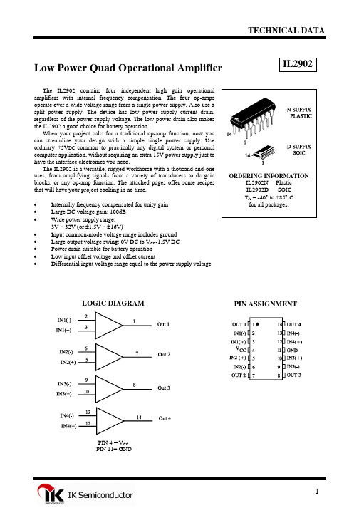
TECHNICAL DATAIL2902Low Power Quad Operational AmplifierThe IL2902 contains four independent high gain operational amplifiers with internal frequency compensation. The four op-amps operate over a wide voltage range from a single power supply. Also use a split power supply. The device has low power supply current drain, regardless of the power supply voltage. The low power drain also makes the IL2902 a good choice for battery operation.When your project calls for a traditional op-amp function, now you can streamline your design with a simple single power supply. Use ordinary +5V DC common to practically any digital system or personal computer application, without requiring an extra 15V power supply just to have the interface electronics you need.The IL2902 is a versatile, rugged workhorse with a thousand-and-one uses, from amplifying signals from a variety of transducers to dc gain blocks, or any op-amp function. The attached pages offer some recipes that will have your project cooking in no time. • Internally frequency compensated for unity gain • Large DC voltage gain: 100dB • Wide power supply range:3V ~ 32V (or ±1.5V ~ ±16V) • Input common-mode voltage range includes ground • Large output voltage swing: 0V DC to V CC -1.5V DC • Power drain suitable for battery operation • Low input offset voltage and offset current • Differential input voltage range equal to the power supply voltageLOGIC DIAGRAMPIN 4 = V CC PIN 11= GNDPIN ASSIGNMENTMAXIMUM RATINGS*Symbol Parameter ValueUnit V CC Power Supply VoltagesSingle Supply Split Supplies32±16VV IDR Input Differential Voltage Range (1) ±32 VV ICR Input Common Mode Voltage Range -0.3 to 32 VI SC Output Short Circuit Duration ContinuousT J JunctionTemperaturePlastic Packages 150 °CTstg StorageTemperaturePlastic Packages -55 to +125°CI IN Input Current, per pin (2) 50 mAT L Lead Temperature, 1mm from Case for 10 Seconds 260 °C*Maximum Ratings are those values beyond which damage to the device may occur.Functional operation should be restricted to the Recommended Operating Conditions.+Derating - Plastic DIP: - 10 mW/°C from 65° to 125°CSOIC Package: : - 7 mW/°C from 65° to 125°CNotes:1.Split Power Supplies.2.V IN<-0.3V. This input current will only exist when voltage at any of the input leads is driven negative.RECOMMENDED OPERATING CONDITIONSSymbol Parameter MinMaxUnitV CC DC Supply Voltage ±2.5 or5.0 ±15 or30VT A Operating Temperature, All Package Types -40 +85 °CThis device contains protection circuitry to guard against damage due to high static voltages or electric fields. However, precautions must be taken to avoid applications of any voltage higher than maximum rated voltages to this high-impedance circuit. For proper operation, V IN and V OUT should be constrained to the range GND≤(V IN or V OUT)≤V CC.Unused inputs must always be tied to an appropriate logic voltage level (e.g., either GND or V CC). Unused outputs must be left open.DC ELECTRICAL CHARACTERISTICS (T A=-40 to +85°C)GuaranteedLimit Symbol Parameter Test Conditions Min Typ Max UnitV IO Maximum Input OffsetVoltage V O=1.4V V CC=5.0-30V;R S=0ΩV ICM=0V to V CC-1.7V9.05.0*mV∆V IO/∆T Input Offset VoltageDriftR S=0Ω, V CC=30V 7.0 µV/°CI IO Maximum Input OffsetCurrent V CC=5.0V15050*nA∆I IO/∆T Input Offset CurrentDriftR S=0Ω, V CC=30V 10 pA/°CI IB Maximum Input BiasCurrent V CC=5.0V500250*nAV ICR Input Common ModeVoltage Range V CC=30V 028VI CC Maximum Power SupplyCurrent R L=∞,V CC=30V,V0=0VR L=∞,V CC=5V,V0=0V31.2mAA VOL Minimum Large SignalOpen-Loop Voltage Gain V CC=15V, R L≥2KΩ1525*V/mVV OH Minimum Output High-Level Voltage Swing V CC=30V,R L=2KΩV CC=30V,R L=10KΩ2627VV OL Maximum Output Low-Level Voltage Swing V CC=5V,R L=10KΩ20mVCMR CommonModeRejectionV CC=30V, R S=10KΩ65* dBPSR Power Supply Rejection V CC=30V 65*dB CS Channel Separation f=1KHz to 20KHz,V CC=30V -120*dBI SC Maximum Output ShortCircuit to GND V CC=5.0V60*mAI source Minimum Output SourceCurrent V IN+=1V, V IN-=0V, V CC=15V,V0=0V10 mAI sink Minimum Output SinkCurrent V IN+=0V, V IN-=1V, V CC=15V,V0=15VV IN+=0V, V IN-=1V, V CC=15V,V0=0.2V510*12*mAµAV IDR DifferentialInputVoltage Range All V IN≥GND or V-Supply (ifused)V CC* V*=@25°CTYPICAL PERFORMANCE CHARACTERISTICSFigure 1.Input Voltage RangeFigure 2. Open-Loop FrequencyFigure 3. Large-Signal Frequency ResponseResponse (Noninverting)Figure 5. Power Supply Current versus PowerSupply VoltageFigure 6. Input Bias Current versus Power SupplyVoltage。

LM2902四运放数据手册
LM324, LM324A, LM324K, LM324KA, LM2902, LM2902V 四运放数据手册
特点:
, 2kVESD保护(后缀为K的器件)
, 宽电源电压范围:
, 单电源...3V到32V(LM2902为26V)
, 双电源...?1.5V到?16V(LM2902为?13V)
, 低源电流漏极,独立于电源电压...典型值为0.8mA , 共模输入电压范围,包括地,允许直接近地测量 , 低输入偏置和补偿参数:
, 输入补偿电压...典型值3mV,A版本的典型值为2mV
, 输入补偿电流...典型值2nA
, 输入偏置电流...典型值20nA,A版本的典型值为15nA , 差动输入电压范围等于最大额定电源电压...32V(LM2902为26V) , 开环差动电压放大...典型值100V/mV
引脚分配
说明
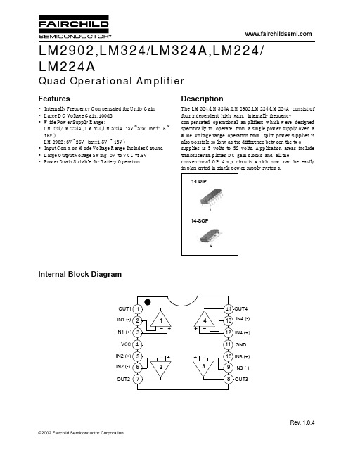
这些器件包含四个独立的高增益频率补偿的运算放大器,主要用于宽范围电源电压的应用。
如果两个电源之差在3V到12V(LM2902为3V到26V)之间,而且VCC 至少比输入共模电压大1.5V,那么使用两个分离电源供电也是可以的。
低源电流漏极独立于源电压的幅度。
应用包括传感器放大器,直流放大模块,以及传统的运放电路,现在可以用单电源电压系统更简单地实现。
例如,在数字系统中LM124可以直接以标准的5V电源供电,非常方便地提供所需的接口要求,而无需?15V电源。
符号(每个放大器)
图1. 单位增益放大器
图2. 噪声测试电路。
SD2902RF POWER TRANSISTORSHF/VHF/UHF N-CHANNEL MOSFETss GOLD METALLIZATIONs COMMON SOURCE CONFIGURATION s 2 - 500 MHz s 15 WATTS s 28 VOLTSs 12.5 dB MIN. AT 400 MHzs CLASS A OR AB OPERATIONsEXCELLENT THERMAL STABILITYDESCRIPTION The SD2902 is a gold metallized N-Channel MOS field-effect RF power transistor. It is intended for use in 28 V DC large signal applications up to 500 MHzNovember 1999ABSOLUTE MAXIMUM RATINGS (T case = 25 o C)THERMAL DATA®1/8SD2902ELECTRICAL SPECIFICATION (T case = 25 o C)STATICREF. 1021308K DYNAMICIMPEDANCE DATACapacitance vs Drain-Source VoltageDrain Current vs Gate VoltageMaximum Thermal Resistance vs Case TemperatureGate-Source Voltages vs Case TemperatureTYPICAL PERFORMANCESD2902Output Power vs Input PowerOutput Power vs Input PowerOutput Power vs Voltage SupplyOutput Power vs Gate VoltagePower Gain vs Output PowerEfficiency vs Output PowerTYPICAL PERFORMANCE SD2902SD2902 400 MHz Test Circuit Schematic400 MHz Test Circuit Component Part ListSD2902400 MHz Test Circuit PhotomasterProduction Test FixtureSD2902Information furnished is believed to be accurate and reliable. However, STMicroelectronics assumes no responsibility for the consequences of use of such information nor for any infringement of patents or other rights of third parties which may result from its use. No license is granted by implication or otherwise under any patent or patent rights of STMicroelectronics. Specification mentioned in this publication are subject to change without notice. This publication supersedes and replaces all information previously supplied. STMicroelectronics products are not authorized for use as critical components in life support devices or systems without express written approval of STMicroelectronics.The ST logo is a trademark of STMicroelectronics© 1999 STMicroelectronics – Printed in Italy – All Rights ReservedSTMicroelectronics GROUP OF COMPANIESAustralia - Brazil - China - Finland - France - Germany - Hong Kong - India - Italy - Japan - Malaysia - Malta - Morocco - Singapore - Spain - Sweden - Switzerland - United Kingdom - U.S.A..SD2902分销商库存信息: STMSD2902。
1Features➤Safely charges two rechargeable alkaline batteries such as Re-newal ®from Rayovac ®➤Terminates pulsed charge with maximum voltage limit ➤Contains LED charge status out-put ➤Features a pin-selectable low-battery cut-off➤Pre-charge qualification indicates fault condition ➤Available in 8-pin 300-mil DIP or 150-mil SOICGeneral DescriptionThe bq2902is a low-cost charger for rechargeable alkaline batteries such as Renewal ®batteries from Rayovac ®.The bq2902combines sensitive,full-charge detection for two recharge-able alkaline cells,with a low-battery cut-off for overdischarge protection.Designed for system integration into a two-cell system,the bq2902can improve the service life of the rechargeable alkaline cells by prop-erly managing the charge and dis-charge.The bq2902requires a voltage limited current source to generate the proper charge pulses for the Renewal ®cell.Each cell is individually monitored to ensure full charge without a damaging overcharge.Charge completion is indicated when the average charge rate falls below approximately 3%of the fast charge rate.A status output is pro-vided to indicate charge in progress,charge complete,or fault indication.The bq2902avoids over-depleting the battery by using the internal end-of-discharge control circuit.The bq2902also eliminates the external power switching transis-tors needed to separately charge individual Renewal cells.For safety,charging is inhibited if the per-cell voltage is greater than 3.0V during charge (closed-circuit voltage),or if the cell voltage is less than 0.4V (open-circuitvoltage).Rechargeable Alkaline Charge/DischargeController ICbq29025/99 C1PN290201.eps8-Pin Narrow DIPor SOIC2348765V SEL BAT 1N BAT 1PDCCHG V SS V SS LRTNDC Charging supply input CHG Battery status outputBAT 1PBattery 1 positive input BAT 1NBattery 1 negative inputV SSBattery 2 negative input IC groundLRTNSystem load returnV SELEnd-of-discharge voltage select input Pin NamesPin ConnectionsPin DescriptionsDC DC supply inputThis input is used to charge the rechargeablealkaline cells and power the bq2902duringcharge.To charge the batteries,this inputshould be connected to a current-source lim-ited to300mA.If the DC input current isgreater than300mA,the power dissipationlimits of the package may be exceeded.TheDC input should also be capable of supplyinga minimum of3.3V and should not exceed5.5V.CHG Charge statusThis open-drain output is used to signify thebattery charging status and is valid onlywhen DC is applied.V SEL End-of-discharge select inputThis three-level input selects the desiredend-of-discharge cut-off voltage for thebq2902.V SEL=BAT1P selects an EDV of1.10V.V SEL floating selects EDV=1.0V.V SEL=V SS selects EDV=0.9.VBAT1P Battery1positive inputThis input connects to the positive terminalof the battery designated BAT1(see Figure3).This pin also provides power to the bq2902when DC is not present.BAT1N Battery1negative inputThis input connects to the negative terminalof the battery designated BAT1(see Figure3).V SS Battery2negative input/IC groundThis input connects to the negative terminalof the battery designated BAT2(see Figure3).LRTN Load returnThis open-drain pull-down output is typi-cally used as a low-side switch.High-sideload switching is also possible with the addi-tion of an external P-FET.Functional DescriptionFigure1is a block diagram outlining the major compo-nents of the bq2902.Figure2illustrates the charge control and display status during a bq2902cycle.Table1outlines the vari-2bq2902Figure 1. Functional Block Diagramous operational states and their associated conditions which are described in detail in the following section. Figure3is an application example.Charge InitiationThe bq2902always initiates and performs a charge cycle whenever a valid DC input is applied.A charge cycle consists of pulse charging the battery and then checking for a termination condition.The charging section ex-plains charging in greater detail.Charge Pre-QualificationAfter DC is applied,the bq2902checks the open-circuit voltage(V OCV)of each cell for an undervoltage condition (V MIN=0.4V)and begins a charge cycle when the V OCV of all cells is above V MIN.If V OCV of any cell is below V MIN,the bq2902enters a charge-pending mode and in-dicates a fault condition(see Table1).The bq2902re-mains in a charge-pending mode until V OCV of each cell is above V MIN.Charge TerminationOnce a charge cycle begins,the bq2902terminates charge when the average charge rate falls below3%of the maximum charge rate.The bq2902also terminates charge when the closed-circuit voltage(V CCV)of any cell exceeds3.0V(V FLT)during charge and indicates a fault condition on the CHG output(see Table1).Charge Re-InitiationIf DC remains valid,the bq2902suspends all charge activity after full-charge termination.A charge cycle is re-initiated when all cell potentials fall below1.4V.The rechargeable alkaline cells,unlike other rechargeable chemistries,do not require a maintenance charge to keep the cells in a fully charged state.The self-discharge rate for the Renewal cells is typically4%per year at room temperature.Charge Status IndicationTable1and Figure2outline the various charge action states and the associated BAT1P,and CHG output states.The charge status output is designed to work with an LED indicator.In all cases,if DC is not present at the DC pin,or if the DC supply is less than the volt-age at the BAT1P pin,the CHG output is held in a high-impedance condition.ChargingThe bq2902controls charging by periodically connecting the DC current-source to the battery stack,not to the in-dividual battery cells.The charge current is pulsed from the internal clock at approximately a80Hz rate on the BAT1P pin.The bq2902pulse charges the battery for approximately 10ms of every12.5ms,when conditions warrant.The bq2902measures the open-circuit voltage(V OCV)of each battery cell during the idle period.If a single-cell poten-3bq2902Notes: 1.V OCV= Open-circuit voltage of each cell between positive and negative leads.2.V CCV= Closed-circuit voltage.Table1.bq2902 Operational Summarytial of any battery is above the maximum open-circuit voltage(V MAX=1.63V±3%),the following pulses are skipped until all cell potentials fall below the V MAX limit.Charging is terminated when the average charge rate falls below approximately3%of the maximum charge rate.Once charging is terminated,the internal charging FET remains off,and the CHG output becomes active per Table1and Figure2.With DC applied,the internal discharge FET will always remain on.End-of-Discharge ControlWhen DC is not present or less than the voltage present on the BAT1P pin,the bq2902power is supplied by the voltage present at the BAT1P pin.In this state,the bat-teries discharge down to the level determined by the V SEL pin.The bq2902monitors the cell voltage of the re-chargeable alkaline cells.If the voltage across any cell is below the voltage speci-fied by the V SEL input,the bq2902disconnects the bat-tery stack from the load by turning the internal discharge FET off.The discharge FET remains off until either the batteries are replaced or DC is reapplied,ini-tiating a new charge cycle.After disconnecting the bat-tery stack from the load,the standby current in the bq2902is reduced to less than1µA.The end-of-discharge voltage(V EDV)is selectable by connecting the V SEL pin as outlined in Table2.Typically,higher dis-charge loads(>200mA)should use a lower discharge voltage cut-off to maximize battery capacity.4bq2902End-of-Discharge Voltage Pin Connection1.10V V SEL= BAT1P1.00V V SEL= Z0.90V V SEL=V SSTable 2.bq2902EDV SelectionsFigure 2.bq2902 Application Diagrambq2902Figure 3.bq2902 Application Example,1.0V EDV5bq2902Absolute Maximum RatingsSymbol Parameter Minimum Maximum Unit NotesDC IN V DC relative to GND-0.37.0VV T DC threshold voltage applied on anypin,excluding the DC pin,relative toGND-0.37.0VT OPR Operating ambient temperature0+70°C Commercial -40+85°C IndustrialT STG Storage temperature-40+85°CT SOLDER Soldering temperature-+260°C10 sec max.I DC DC charging current-400mAI LOAD Discharge current-500mAI OL Output current--mA CHGNote:Permanent device damage may occur if Absolute Maximum Ratings are exceeded.Functional operation should be limited to the Recommended DC Operating Conditions detailed in this data sheet.Exposure to con-ditions beyond the operational limits for extended periods of time may affect device reliability.DC Thresholds(T A= 25°C;V DC= 5.5V)Symbol Parameter Rating Tolerance Unit NotesV MAX Maximum open-circuitvoltage 1.63±3%VV OCV>V MAX inhibits/terminatescharge pulsesV EDV End-of-discharge voltage 0.90±5%V V SEL= BAT2N1.00±5%V V SEL= Z1.10±5%V V SEL= BAT1PV FLT Maximum open-circuitvoltage3.00±5%VV CCV>V FLT terminates charge,in-dicates faultV MIN Minimum battery voltage0.40±5%V V OCV<V MIN inhibits chargeV CE Charge enable 1.40±5%V V OCV<V CE on both cells re-initiates chargeNote:Each DC threshold parameter above has a temperature coefficient associated with it.To determine the coefficient for each parameter,use the following formula:TempcoParameterRating=163.*-0.5mV/°CThe tolerance for these temperature coefficients is 10%.67bq2902DC Electrical Characteristics (T A =T OPR )Symbol ParameterMinimum TypicalMaximum Unit NotesV IH Logic input high V BAT1P - 0.1-V BAT1P V V SEL V IL Logic input low V SS -V SS + 0.1V V SELV OL Logic output low --0.8V I OL =10mA I OL Output current 10--mA @V OL =V SS + 0.8V I CC Supply current --250µA Outputs unloaded,V DC = 5.5VI SB1Standby current --25µA V DC = 0V ,V OCV >V EDV I SB2End-of-discharge standby current --1µA VDC = 0V I L Input leakage --±1µA V SEL I OZ Output leakage in high-Z state -5--µA CHGR DSON On resistance -0.5-ΩDischargeFET;V BAT1P =1.8V I IL Logic input low --70µA V SEL I IH Logic input high -70--µA V SEL I IZ Logic input float -2-2µA V SELI DC DC charging current --300mA V DC DC charging voltage 3.3- 5.5V DC I LOAD Discharge current --400mA V OPOperating voltage1.8- 5.5VBAT 1P Timing(T A =T OPR )Symbol ParameterMinimumTypical MaximumUnit Notest P Pulse period -12.5-ms See Figure 2t PW Pulse width-10-msSee Figure 2Note:Typical is at T A = 25°C.bq2902DE1EC e LGBAA1B1 S8-Pin DIP(PN)8-Pin PN(0.300" DIP)DimensionInches Millimeters Min.Max.Min.Max.A0.1600.180 4.06 4.57A10.0150.0400.38 1.02B0.0150.0220.380.56B10.0550.065 1.40 1.65C0.0080.0130.200.33D0.3500.3808.899.65E0.3000.3257.628.26E10.2300.280 5.847.11e0.3000.3707.629.40G0.0900.110 2.29 2.79L0.1150.150 2.92 3.81S0.0200.0400.51 1.0289bq29028-Pin SOIC Narrow (SN)8-Pin SN (0.150" SOIC )DimensionInchesMillimeters Min.Max.Min.Max.A0.0600.070 1.52 1.78A10.0040.0100.100.25B 0.0130.0200.330.51C 0.0070.0100.180.25D 0.1850.200 4.70 5.08E 0.1500.160 3.81 4.06e 0.0450.055 1.14 1.40H 0.2250.245 5.72 6.22L0.0150.0350.380.89bq2902Data Sheet Revision HistoryChange No.Page No.Description Nature of Change 12Figure 1.Functional Block Diagram Updated block diagram Notes:Change 1 = May 1999 C changes from Jan.1997 B.10bq2902 Ordering Informationbq2902Package Option:PN=8-pin plastic DIPSN=8-pin narrow SOICDevice:bq2902Rechargeable AlkalineCharge/Discharge Controller IC11IMPORTANT NOTICETexas Instruments and its subsidiaries (TI) reserve the right to make changes to their products or to discontinue any product or service without notice, and advise customers to obtain the latest version of relevant information to verify, before placing orders, that information being relied on is current and complete. All products are sold subject to the terms and conditions of sale supplied at the time of order acknowledgement, including those pertaining to warranty, patent infringement, and limitation of liability.TI warrants performance of its semiconductor products to the specifications applicable at the time of sale in accordance with TI’s standard warranty. Testing and other quality control techniques are utilized to the extent TI deems necessary to support this warranty. Specific testing of all parameters of each device is not necessarily performed, except those mandated by government requirements.CERTAIN APPLICATIONS USING SEMICONDUCTOR PRODUCTS MAY INVOLVE POTENTIAL RISKS OF DEATH, PERSONAL INJURY, OR SEVERE PROPERTY OR ENVIRONMENTAL DAMAGE (“CRITICAL APPLICATIONS”). TI SEMICONDUCTOR PRODUCTS ARE NOT DESIGNED, AUTHORIZED, OR WARRANTED TO BE SUITABLE FOR USE IN LIFE-SUPPORT DEVICES OR SYSTEMS OR OTHER CRITICAL APPLICATIONS. INCLUSION OF TI PRODUCTS IN SUCH APPLICATIONS IS UNDERSTOOD TO BE FULLY AT THE CUSTOMER’S RISK.In order to minimize risks associated with the customer’s applications, adequate design and operating safeguards must be provided by the customer to minimize inherent or procedural hazards.TI assumes no liability for applications assistance or customer product design. TI does not warrant or represent that any license, either express or implied, is granted under any patent right, copyright, mask work right, or other intellectual property right of TI covering or relating to any combination, machine, or process in which such semiconductor products or services might be or are used. TI’s publication of information regarding any third party’s products or services does not constitute TI’s approval, warranty or endorsement thereof.Copyright © 1999, Texas Instruments Incorporated。
uc2902d工作原理UC2902D是一款常用的电源管理集成电路,它具有多种功能和广泛的应用领域。
本文将从UC2902D的工作原理、特点和应用场景等方面进行详细介绍。
我们来了解一下UC2902D的工作原理。
UC2902D是一款双路电源管理IC,主要用于电池充电和电池保护。
它采用了电流模式控制和PWM调制技术,能够有效地控制电流和电压的稳定性,实现电池的高效充电和保护功能。
在充电模式下,UC2902D可以根据输入电压和电流的变化来动态调整输出电流和电压,以实现快速充电。
同时,它还具有过流保护和短路保护功能,可以有效地保护电池和充电器的安全性。
在保护模式下,UC2902D可以监测电池的电压和温度等参数,并根据设定值来控制充电和放电过程。
当电池电压超过设定值或温度过高时,UC2902D会自动停止充放电,以保护电池的安全性和寿命。
除了充电和保护功能,UC2902D还具有电池状态监测和电池平衡功能。
它可以实时监测电池的电压和电流等参数,并根据设定值来判断电池的状态。
同时,它还可以通过调节输出电流和电压的差异来实现电池的平衡,以延长电池的使用寿命。
UC2902D具有多种特点和优势。
首先,它采用了先进的控制算法和高效的功率转换技术,能够实现高效充电和保护功能。
其次,它具有丰富的接口和功能,可以方便地与其他设备进行通信和控制。
此外,它还具有小尺寸、低功耗和高可靠性等优点,适用于各种电池应用场景。
UC2902D广泛应用于电子产品、电动车、太阳能电池等领域。
在电子产品领域,UC2902D可以用于手机、平板电脑和笔记本电脑等设备的电池管理和充电控制。
在电动车领域,UC2902D可以用于电动汽车和电动自行车等车辆的电池管理和充电系统。
在太阳能电池领域,UC2902D可以用于太阳能电池板的充电和电池管理。
UC2902D作为一款功能强大的电源管理集成电路,具有多种功能和广泛的应用领域。
通过对其工作原理、特点和应用场景的介绍,相信读者对UC2902D有了更深入的了解。
药过程安全与环保、药品GMP实施与管理、制药工程过程验证、制药自动化与智能制造。
实习实训:对接真实职业场景或工作情境,在校内外进行药品生产质量管理、工程管理、药品生产综合技能、工艺验证、设备管理和维护等实训。
在医药生产企业等单位进行岗位实习。
职业类证书举例职业资格证书:执业药师职业技能等级证书:药物制剂生产接续专业举例接续专业硕士学位授予领域举例:制药工程、生物与医药接续硕士学位二级学科举例:药学专业代码290202专业名称药品质量管理基本修业年限四年职业面向面向质量管理工程技术人员等职业,GMP管理、验证管理、药品检查等岗位(群)。
培养目标定位本专业培养德智体美劳全面发展,掌握扎实的科学文化基础和药品GMP实施与管理、质量风险管理与验证、药品检查技巧及相关法律法规等知识,具备药品生产全过程质量管理、验证项目实施与管理、质量管理体系文件检查和现场检查等能力,具有工匠精神和信息素养,能够从事GMP管理、验证管理、药品检查等工作的高层次技术技能人才。
主要专业能力要求1. 具有对药品生产全过程进行现场质量管理的能力;2. 具有对药品生产检验场所、活动进行风险研判和风险控制的能力;3. 具有药品质量管理体系建立、运行和持续改进的能力,能够实施文件管理、偏差和变更管理、质量控制实验室管理等质量管理活动;4. 具有按照国内外GMP和质量管理体系要求开展内部自检、外部审计以及迎接GMP检查的能力;1745. 具有掌握药品检查技巧,按照法律法规和药品检查方案要求,实施文件检查、现场检查等检查活动及相关指导的能力;6. 具有验证管理体系构建、验证项目实施和管理的能力;7. 具有运用综合理论知识,发现、分析和解决复杂质量问题,协助开展药品质量管理领域研发和创新发展的能力;8. 具有掌握绿色生产、环境保护、安全防护、质量管理等相关政策要求的能力;9. 具有适应数字经济发展新需求,学习新知识、新技术的能力;10. 具有探究学习、终身学习和可持续发展的能力。
2902#6345#现代企业管理方法复习意见
一、考核对象
本课程的考核是针对行政管理专科的选修学生,考核代码是2902(开卷)6345(闭卷)。
二、考核目标
课程的考核是进一步强化教学过程、保证学习质量、落实教学成果、达到学习目标的重要教学环节,可以引导学生在学习过程中正确理解把握所学课程的内容。
通过考核既要检测学生对现代企业管理方法基本理论知识的掌握,更重要的是考核学生对基本知识的运用,提高学生分析问题和解决问题的能力。
三、考核方式
本课程考核采用形成性考核与终结性考核相结合的方式。
形成性考核是在学习过程中根据学习进度进行的各种形式的考核,有利于学生随时检查学习状况,及时查漏补缺,更好地掌握所学内容。
每次形成性考核任务涉及课程的核心内容,力争通过完成任务的过程掌握课程的主要内容,提高分析应用能力。
形成性考核有案例分析、社会调查、小组讨论、网上学习、实践等多种形式。
学生参加网上学习、实时或非实时讨论发言,按照规定上交作业,均可获得形成性考核成绩。
终结性考核参加省电大组织的统一期末考试,使用纸制试卷,终结性考核是对课程学习结果的考核,重点考查基本知识、基本理论的掌握情况,覆盖课程全部内容,实行开卷考试。
题型和比例一般为:单选题(20%)、计算题(50%)、论述题(10%)、案例分析题(20%)。
考试时间为90分钟。
四、考核组织
形成性考核要将考核与教学过程有机地结合起来。
通过形成性考核,一方面可以加强对地方电大教师教学过程的引导、指导和管理,优质的完成教学任务,实现教学目标;另一方面可以加强对学生平时自主学习过程的指导和监督,重在对学生自主学习过程进行的指导和检测,引导学生按照教学要求和自主学习计划完成学习任务,达到掌握知识、提高能力的目标;再一方面推进对学生综合素质的训练和提高,使学生能够运用所掌握的现代企业管理方法知识分析指导实际经济活动,重点使学生的动手能力得以提高。
省电大在课程教学实施方案里规定了形成性考核所涉及的基本内容、考核方式等基本要求,由各分校的教师根据实际情况适当加以细化、提出进一步的要求。
形成性考核的设计要充分考虑结合个人进行的社会实践活动,课堂讨论(网上讨论)、小组活动等内容,全方位的考查学生学习的情况。
五、考核成绩
本课程形成性考核占课程考核成绩的20%,终结性考核占考核成绩的80%。
形成性考核成绩与终结性考核成绩分别为百分制,最后按比例记入总成绩,共同构成本课程的考核成绩。
形成性考核每次任务的成绩要考虑学生在活动中的表现综合考评。
具体所占比例,各分校可以根据实际情况考虑。
六、考核重点
1.简单了解企业的定义
2.了解公司制企业的类型
3.掌握现代企业制度的定义及其特征
4.了解企业管理的含义,并了解相关的管理理论。
5.掌握企业文化的形成与发展,以及企业文化的功能
6.组织的构成及要素,组织结构设计的原则
7.掌握组织结构的各种模式,并了解其优缺点
8.了解人力资源的定义及特点
9.简单了解德尔菲法
10.掌握经营决策的概念及特点
11.重点掌握经营决策的各种方法及其计算
12.了解企业战略的概念
13.熟悉企业战略的分类及其适用条件
14.了解产品组合策略
15.了解ISO9000系列及全面质量管理
16.掌握学习型组织的定义及其特征
七、举例
某房地产集团属下一家物业经营管理公司,成立初期,该公司非常注重管理的规范化和充分调动员工积极性,制定了一套较科学完善的薪酬管理制度,公司得到了较快的发展,短短的两年多时间,公司的业务增长了110%。
随着公司业务的增加和规模的扩大,员工也增加了很多,人数达到了220多人。
但公司的薪酬管理制度没有随公司业务发展和人才市场的变化而适时调整,还是沿用以前的。
公司领导原以为公司的发展已有了一定的规模,经营业绩理应超过以前,但事实上,整个公司的经营业绩出现不断滑坡,客户的投诉也不断增加,员工的工作失去了往日的热情,出现了部分技术、管理骨干离职,其他人员也出现不稳定的预兆。
其中:公司工程部经理在得知自己的收入与后勤部经理的收入相差很少时,感到不公平,他认为工程部经理这一岗位相对后勤部经理,工作难度大、责任重,应该在薪酬上体现出这种差别,所以,工作起来没有了以前那种干劲,后来辞职而去。
因为员工的流失、员工工作缺乏积极性,致使该公司的经营一度出现困难。
在这种情况下,该公司的领导意识到问题的严重性,经过对公司内部管理的深入了解和诊断,发现问题出在公司的薪酬系统上,而且关键的技术骨干力量的薪酬水平较市场明显偏低,对外缺乏竞争力;公司的薪酬结构也不尽合理,对内缺乏公平,从而导致技术骨干和部分中层管理人员流失。
针对这一具体问题,该公司就薪酬水平进行了市场调查和分析,并对公司原有薪酬制度进行调整,制定了新的与企业战略和组织架构相匹配的薪资方案,激发了员工的积极性和创造性,公司发展又开始恢复良好的势头。
请运用所学的理论,对以上问题进行分析。
考核目的:案例分析是提高学生分析问题和发现问题的重要方法之一。
通过下面的案例分析,既可以加深学生对薪酬理论问题的理解与把握,学会分析问题的方法和技巧,扩大知识面,提高学习兴趣;也有利于同学们掌握薪酬设计地基本原理。
解题思路:
(1)分析薪酬设计的特点及过程;
(2)从民营企业的角度进行分析;
(3)从薪酬设计的层次进行分析;
(4)从薪酬设计的原则性进行分析。
(5)联系案例进行发挥。