LC串联谐振变换器与LLC谐振变换器的 分析与比较
- 格式:docx
- 大小:26.53 KB
- 文档页数:2
LLC谐振变换器的原理说明LLC谐振变换器要提⾼主变换器能效,可以采⽤以下四种⽅式:⼀是降低导通损耗或者是减⼩初级峰值电流和均⽅根电流来降低⼀次导通损耗;⼆是采⽤软开关技术降低开关损耗;三是减⼩整流器的压降,例如采⽤低的正向压降⼆极管或者FET整流器,来降低⼆次损耗; 四是采⽤更好的磁芯材料来降低磁芯损耗.杨恒.LED照明驱动器设计步骤详解[M].北京:中国电⼒出版社.20101软开关技术的提出(电⼒电⼦技术-西安交通⼤学王兆安黄俊第四版)还是从⼩型化、轻量化的发展趋势看,装置的效率以及电磁兼容的要求变得更⾼。
当提⾼开关频率,开关损耗增加,电路的效率下降,电磁⼲扰也增⼤,这⾥提出了软开关技术,它是利⽤谐振的辅助换流⼿段,从⽽解决电路的开关损耗和开关噪声的问题。
硬开关:开关过程中,电压电流均不为零,出现重叠,因此导致开关损耗(电路效率的降低、阻碍开关频率的提⾼)。
并且,电流电压变化很快,波形有明显的过冲,导致了开关噪声(电磁⼲扰EMI)。
如图5-1所⽰:图5-1 硬开关电路波形软开关:通过增加电感、电流等谐振元件,构成辅助换流⽹络,在开关过程的前后引⼊谐振过程。
开关开通前电压降为零,或者关断之前电流降为零,消除电压电流之间的重叠,降低电压电流的变化率,减⼩开关损耗和开关噪声。
如图5-2所⽰:图5-2 软开关电路波形主要的软开关拓扑结构有:结合本⽂设计要求,将采⽤双电感加单电容的谐振变换器。
2谐振变换器的发展为了降低开关损耗和开关噪声,并且容许⾼频运⾏,谐振开关技术得到了发展。
在各类的谐振变换器中,LC串联谐振变换器是最简单也是最普遍的。
1)LC串联谐振变换器电路中电感与电容串联,形成⼀个串联谐振腔。
这个谐振腔的阻抗与负载串联,则由于其串联分压作⽤,增益总是⼩于1。
谐振腔的阻抗与频率有关,在其谐振频率fr下阻抗最⼩,此时的增益也最⼤。
根据电路的直流特性可知:① fs>fr时,开关管 Q-->ZVS;②轻载时,fs要变化很⼤才能保证输出电压不变;③ Vin增⼤时,fs增⼤使输出电压保持不变。
LLC串联谐振全桥DCDC变换器的研究移相全桥和LLC区别LLC串联谐振全桥DC-DC变换器是一种高效率的电力转换器,在许多应用中被广泛使用。
它可以实现高频率的电力转换,并具有快速的动态响应和低噪声特性。
与传统的移相全桥变换器相比,LLC变换器具有以下几点不同之处。
首先,移相全桥变换器是一种自振变换器,它的输出电压和输入电压之间的变换是通过改变谐振电感的相位来实现的。
这种变换方式能够提供高效率,但在高转换比时可能会出现电压换流问题。
而LLC变换器采用串联谐振网络,可以消除电压换流问题,并且提供更稳定的输出电压。
其次,移相全桥变换器的控制方式是通过改变谐振电感的频率来控制输出电压和输入电压之间的变换。
这种频率调制可以实现精确的电压调节,但需要更复杂的控制算法。
而LLC变换器采用谐振电容和谐振电感的并联谐振,能够通过改变谐振频率来实现精确的电压调节。
同时,LLC变换器的控制方式更简单,可轻松实现开环或闭环控制。
此外,LLC变换器还具有更低的开关损耗和更高的功率密度。
由于谐振网络可以在零电压或零电流点进行开关切换,因此LLC变换器的开关频率可以设置得相对较高,从而减少开关损耗。
与此同时,LLC变换器的谐振网络能够实现较高的功率密度,因为它可以有效地利用电流和电压的变化。
最后,LLC变换器还具有较低的EMI噪声和较少的谐振峰。
由于LLC变换器采用谐振网络,可以在零电压或零电流点进行开关切换,从而减少开关干扰和EMI噪声。
与此同时,LLC变换器还能够通过调节谐振频率来抑制谐振峰,从而减少谐振峰对系统的影响。
综上所述,LLC串联谐振全桥DC-DC变换器相对于传统的移相全桥变换器具有更稳定的输出电压、更简单的控制方式、更低的开关损耗和更高的功率密度。
因此,在高效率、高转换比和高功率密度的应用中,LLC变换器通常是更为理想的选择。
LLC串联谐振全桥DCDC变换器的研究LLC串联谐振全桥DC/DC变换器的工作原理是将全桥拓扑结构与LLC 谐振拓扑结构相结合。
变换器的输入端采用全桥结构,输出端采用谐振电路结构。
在输入端,通过控制两个辅助开关的开通和关闭,实现了相对零电压开关和相对零电流开关。
在输出端,谐振电路由电容、电感和电阻构成,通过控制开关管的导通和关断,实现了谐振振荡。
通过这样的工作原理,LLC串联谐振全桥DC/DC变换器可以实现高效率的功率转换。
LLC串联谐振全桥DC/DC变换器具有一系列优点。
首先,由于采用了全桥结构,输入电压范围广泛,可以适应各种不同的电源。
其次,由于采用了LLC谐振结构,能够实现高效并且低噪音的输出。
此外,该变换器还具有可调性好、响应速度快、波形质量高、设计简单等优点。
在研究LLC串联谐振全桥DC/DC变换器时,可以从以下几个方面进行深入研究:1.拓扑结构设计:根据应用需求,设计适合的LLC串联谐振全桥DC/DC变换器拓扑结构,选择合适的电阻、电容和电感等元器件。
2.开关管选择与控制:选择合适的开关管,并设计合理的开关管控制策略,实现零电流开关和零电压开关。
3.谐振电路设计:设计合适的谐振电路,包括电容、电感和电阻的参数选择,以及谐振频率和谐振频率范围的确定。
4.功率转换效率研究:研究LLC串联谐振全桥DC/DC变换器的功率转换效率,分析其与输入电压、输出电压、负载等因素的关系,优化变换器性能。
5.控制策略研究:研究合适的控制策略,实现LLC串联谐振全桥DC/DC变换器的稳定工作,提高系统动态响应性能。
除了理论研究,还可以进行仿真和实验验证。
利用软件仿真工具,如Matlab/Simulink、PSIM等,进行LLC串联谐振全桥DC/DC变换器的性能分析和优化。
并且利用实验平台,搭建LLC串联谐振全桥DC/DC变换器的实验系统,验证理论研究成果的正确性。
总结来说,LLC串联谐振全桥DC/DC变换器是一种高效率、高性能的直流-直流变换器。
了解LLC在谐振应用中的结构谐振式LLC拓朴,串联谐振式变换器(SRC)中的成员开始广泛地应用于消费类电子产品中,如LCD TV及PDP电视。
在这些应用中,需要高的安全性,可靠性及低的EMI,防止产品在移动及工作中失效。
为面对这些挑战,ONSEMI给出了新款的控制器NCP1395(低压驱动)和NCP1396(高压驱动),致力于推动LLC型谐振电源。
当然,在此设计之前,要先了解谐振式电路结构及应用注意。
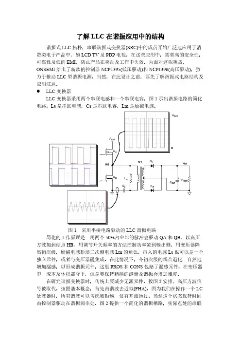
LLC变换器LLC变换器采用两个串联电感和一个串联电容,图1示出谐振电路的简化电路。
Ls是串联电感,Cs是串联电容,Lm是励磁电感。
图1 采用半桥电路驱动的LLC谐振电路简化的工作原理是:用两个50%占空比的脉冲去驱动QA和QB,以高压方波加到结点HB,用调节开关频率的方法控制功率流到输出侧,用变压器隔离初次级,励磁电感扮演二次侧电感Lm的角色,串入的电感Ls也可以是一个独立元件,或者与变压器磁集成。
在此情况下,令初次级的耦合退化,自然地增加漏感,以形成谐振元件,这里PROS和CONS包括了漏感元件。
在变压器中,成本及体积都降下,但是要保持精确的感量及谐振会增加难度。
在研究谐振变换器时,传统上要减少无源元件。
按图2安排,高压方波信号被取代。
按照基本概念,首先由谐波去近似(FHA)。
因为我们在操作一个LC 滤波器时,所有谐波可以考虑被拒绝,仅有基波通过。
当然这个状态保持时间由控制器驱动在谐振频率处。
图2提供一个简化的谐振槽路,实际点处的串联阻抗(Ls和Cs) 还要与对应负载并联。
图2 LLC谐振电路的实际阻抗网络谐振频率在两个不同的频率之间变化,取决于负载大小。
1,R L=0,短路,Lm消失,Zseries为短路,串联谐振点为:(1)在Fsw = Fs处,Zseries变为短路,AC传输功能降到1 (或0db)。
2,R L = ∞,轻载或空载条件下,Lm以与Ls串联形式出现,整个网络谐振在Fmin处。
串并联谐振电路的区别详解
串联谐振电路指的是,在电子串联电路中电阻、电感以及电容出现电压、电流和电源相同相位角度情况下的现象,称为电子电路串联谐振电路。
串联谐振电路的特点是:串联谐振电路呈纯电阻性,电源、电压和电流同相位,此时,电抗等于0,阻抗等于电阻R,电路的阻抗最小,电流最大,谐振电压与原本相互电压叠加,在电感和电容上产生比电源输出电压高出很多倍的高电压,因此,串联谐振电路也称电压谐振试验项目。
并联谐振电路指的是,在电阻、电感和电容并联电路中,出现电路端电压和总电流相位相同角度的现象,称为电子电路并联电路。
并联电路的原理特点是:并联谐振是一种完全的补偿电路,电源不需要提供无功功率,只提供并联电路中电阻所需要的有功功率,输出产生谐振电路时,并联电路产生的总电流最小,此时,支路电流大于电路中的总电流,因此,并联谐振电路也叫并联谐振或者是电流谐振。
串联谐振、并联谐振试验设备,可同时满足电力变压器、交联电缆、开关柜、电动机、发电机、GIS 全气体绝缘组合电器设备和SF6开关、母线、电容套管、充油套管、电流互感器(CT)、电压互感器(PT)等试验对象的的(工频)交流耐压试验,串联谐振、并联谐振试验设备是复合型交流耐压设备。
华天电力专业生产串联谐振耐压装置,从事电测行业多年,旗下产品品质一流,欢迎广大客户前来选购。
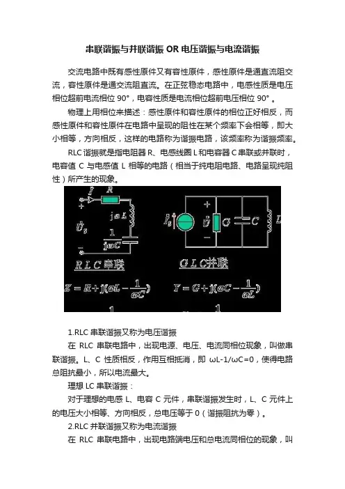
串联谐振与并联谐振OR电压谐振与电流谐振交流电路中既有感性原件又有容性原件,感性原件是通直流阻交流,容性原件是通交流阻直流。
在正弦稳态电路中,电感性质是电压相位超前电流相位90°,电容性质是电流相位超前电压相位90° 。
物理上用相位来描述:感性原件和容性原件的相位正好相反,而感性原件和容性原件在电路中呈现的阻性在某个频率下会相等,即大小相等,方向相反,这样的电路称为谐振电路,该频率称为谐振频率。
RLC谐振就是指电阻器R、电感线圈L和电容器C串联或并联时,电容值C与电感值L相等的电路(相当于纯电阻电路、电路呈现纯阻性)所产生的现象。
1.RLC串联谐振又称为电压谐振在RLC 串联电路中,出现电源、电压、电流同相位现象,叫做串联谐振。
L、C 性质相反,作用互相抵消,即ωL-1/ωC=0,使得电路总阻抗最小,所以电流最大。
理想LC串联谐振:对于理想的电感L、电容C元件,串联谐振发生时,L、C元件上的电压大小相等、方向相反,总电压等于0(谐振阻抗为零)。
2.RLC并联谐振又称为电流谐振在RLC 串联电路中,出现电路端电压和总电流同相位的现象,叫做并联谐振。
L、C 性质相反,作用互相抵消,即1/ωL-ωC=0,使得电路总导纳最小,所以电压最大。
理想LC并联谐振:对于理想的L、C元件,并联谐振发生时,L、C元件中的电流大小相等、方向相反,总电流等于0(谐振阻抗为无穷大)。
故称为电流谐振。
3.能量交换无论是串联谐振还是并联谐振,在谐振发生时,电感L和电容C 之间都实现了完全的能量交换。
即电感释放的磁能完全转换成电场能储存进电容;而在另一时刻电容放电,又转换成磁能由电感储存。
在串联谐振电路中,由于是串联,电感L和电容C流过的市同一个电流,因此能量的交换以电压极性的变化进行。
其特点是:电路呈纯电阻性,电源、电压和电流同相位,此时电路的阻抗最小,电流最大,在电感和电容上可能产生比电源电压大很多倍的高电压,因此串联谐振也称电压谐振。
串联谐振变换器和并联谐振变换器好嘞,今天咱们就聊聊串联谐振变换器和并联谐振变换器。
听起来是不是挺高大上的?听起来复杂,实际也就是个简单的电气玩意儿。
想象一下,你在参加一个聚会,现场音乐嘈杂,结果你却被一首歌吸引住了,浑身心都跟着那旋律起伏。
这种现象就跟谐振器的工作原理类似,好的谐振器能把特定频率的信号“放大”,让你听得特别清晰。
而串联和并联的区别呢,就像不同的聚会风格,有些是个别聊天,有些是大家一起热闹。
先说说串联谐振变换器。
想象一下,几个人排成一排,听到一个有趣的笑话,每个人都跟着这个笑话笑,笑声连成一片。
这个时候,笑声就是电流,笑的频率就是电压。
串联的好处在于,当一个部分被激活,整个队伍都跟着一起动。
哎呀,真是“众人拾柴火焰高”,同样的道理,串联谐振变换器能将输入信号的频率增强,使输出信号更加稳定。
但这可不是说简单的连接哦,它们可得有个特定的频率,才能“玩”得开心。
再说并联谐振变换器。
想象一下,一个大圆桌,大家围坐着,各自聊着自己的话题。
每个人的声音虽小,却可以在合适的时机瞬间形成一股强大的力量。
并联谐振变换器就是这样的一个大家庭。
每个部分都独立工作,但又能够在合适的频率下集体合作。
它的强大之处在于,如果其中一个部分出了问题,其他部分还能继续保持运转。
就像聚会上,大家各自交流,没有人会因为某个人的冷场而停下来。
相对来说,它的稳定性更高,可以容忍一定的“骚动”。
说到这里,可能有人会问,为什么要分成串联和并联呢?每种方式都有自己的适用场景,就像人生中,有人喜欢热闹,有人更享受安静。
串联谐振变换器适合需要高增益和频率选择的场合,比如一些高频信号的放大。
而并联谐振变换器则更适合需要高效率和低损耗的场合,比如电源管理,保证系统稳定运行。
使用这些变换器的时候,也得注意“对症下药”。
每种场合都有它的“黄金法则”,可不能随便换。
就像喝酒,开车不喝,喝酒不开。
否则,事儿可就大了。
实际上,理解这些原理并不难,关键在于多做实验,多动手操作。
LLC谐振转换器之分析飞兆半导体特稿2009年6月LLC谐振转换器之分析作者:飞兆半导体欧洲功率转换及工业产品市场开发经理Jon Harper 引言/摘要全球对降低能耗的需求正在促进节能技术的推广。
在70W - 500W交流输入电源中,由于LLC谐振转换器(效率通常在90%以上) 的效率高于标准电源拓扑,所以其运用越来越广泛。
本文阐释了谐振转换器高效的原因,并探讨了LLC谐振转换器的功能和优势,最后简要分析了一个采用FSFR2100 LLC谐振转换器的电源。
采用谐振转换器的理由把能耗降至最低有许多好处:减少温室气体排放;减少不可再生能源的使用,以及降低运行电源的生命周期成本。
电源节能倡议不仅建议或规定不同负载条件下电源的效率,而且还包括了对待机功耗的要求。
在美国加州,50W以上的外部适配器的满负载效率必须大于85%。
80PLUS等自愿性倡议要求电源在20%、50%和100%不同负载条件下的效率都大于80%。
而欧盟正在对20大类产品进行评估,旨在于整个欧洲范围内推出节能规范,在其它地区的既有规范和自愿性标准预计将对欧盟规范有重大影响。
功率因数校正(PFC) 前端是电源常用的一项额外功能,例如80PLUS倡议就要求采用PFC的功能。
PFC可以节省耗电量,避免建筑物内第三阶谐波电流造成的一些问题,而PFC电路一般能产生380V-400V左右的恒定电压,这种窄输入电压范围大大有利于谐振拓扑的采用。
以往,前级临界连续Boost升压PFC和后级双管正激拓补,都是100W – 300W功率因数校正电源的首选拓扑,这种情况直到最近才有所改变。
这种拓扑简明易懂,是隔离型降压拓扑(正激拓扑) 的衍生结构,利用两个晶体管代替一个晶体管,可尽量减小晶体管成本,简化变压器设计。
此外,这种拓扑能够处理很宽的输入电压范围,具有很好的轻负载调节性能。
不过,它需要一个很大的输出电感,在大负载条件下的效率低于谐振转换器。
谐振转换器中的零电压开关谐振转换器的高效率优势源于它采用了零电压开关 (ZVS) 技术 [注1]。
Comparative Study of Half-Bridge LCC and LLC Resonant DC-DC Converters for Ultra-Wide Output Power range ApplicationsSaijun Mao1,3*, Jelena Popovic3, Ramanujam Ramabhadran2,Jan Abraham Ferreira31.GE Global Research, Shanghai, China2.GE Global Research, Niskayuna, US3.Delft University of Technology, Delft, The Netherlands*Tel.: +86 / (21)– 38771302*Fax: +86 / (21)– 50807277*E-Mail: Saijun.Mao@Keywords«LCC resonant converter»,«LLC resonant converter», «Wide output power range», «High efficiency», «Narrow switching frequency range»AbstractThe Half-Bridge (HB) LCC resonant DC-DC converter and HB LLC resonant DC-DC converter circuit are comparatively studied for high efficiency ultra-wide output power range application in this paper. The output voltage ranges from minimum output voltage to twice that value. And the output current ranges from 10% load to 100% load. So the output power spans over a wide range, from minimum to 20 times that. The detailed resonant tank characteristics analysis for HB LCC and LLC resonant converter is provided. Through the 150W hard prototype experiments validation, it is shown that HB LLC resonant DC-DC converter can achieve better performance with flat efficiency, narrow switching frequency range compared with HB LCC resonant DC-DC converter for wide output current application at both 75V & 150V output voltage from 10% output current to 100 % output current conditions. HB LLC resonant DC-DC converter is more preferred power conversion circuit topology to achieve high performance with flat efficiency, narrow switching frequency range in ultra-wide output power range applications.1. IntroductionWith the increasing demand for high efficiency and high power density, the Half-Bridge (HB) LCC resonant DC-DC converter and HB LLC resonant DC-DC converter are 2 most promising isolated topologies achieve high performance power conversion[1-5]. HB LCC resonant DC-DC converter circuit and HB LLC resonant DC-DC converter can both achieve zero voltage switching turn-on for switches when the switching frequency is above the resonant frequency. The HB LCC resonant DC-DC converter and HB LLC resonant DC-DC converter are both used for ultra-wide output power range applications, such as battery charging, and lighting electronics with dimming function [4-8]. Both LCC and LLC resonant DC-DC converters are introduced for wide load range applications respectively [4-8]. In this investigation, the output voltage ranges from the minimum value to twice that value. And the output current is 10 times range from 10% light load to 100% load. So the output power range very wide (20 times). The investigation of the LCC resonant DC-DC converter and LLC resonant DC-DC converter at such ultra-wide output range application is the research motivation to achieve high circuit efficiency with flat efficiency and narrow switching frequency range.The output power specification for this investigation scope is from 75VDC to 150VDC, and outputcurrent specification is from 0.1A to 1A with 450V DC input. The circuit schematics of HB LCC resonant converter is illustrated in Fig.1. The key requirements for design target: flat efficiency curve and tight switching frequency range at wide load range.oo(a) HB LCC Resonant DC-DC Converter (b) HB LLC Resonant DC-DC ConverterFig.1: Schematic of HB Resonant ConverterThe resonant frequency of LCC and LLC resonant tank can be found in equation 1 and 2 respectively.1rf;2rf(1)r f;mf(2)2. LCC & LCC resonant resonant tank characteristics analysisThe design parameters for the HB LCC resonant tank and HB LLC resonant tank can be summarized in Table based on the reference papers [4-8]. The HB LCC & LLC resonant tank gain characteristics curve at 75V and 150V output voltage can be obtained in Fig.2 and Fig.3 respectively.f s/Hz1103u1104u1105u1106uFig.2(a):LCC gain curve at V o=150V1103u1104u1105u1106uf s/HzFig.2(b):LCC Gain curve at V o=75VC p has big impact for LCC resonant converter atV o=150V, the operation frequency is aroundC pC p.M dcV o1104u1105u1106u1107uf s/HzFig. 3(a): LLC Gain curve at V o=150V1104u1105u1106u1107uM dcf s/HzFig. 3(b): LLC Gain curve at V o=75VThe transformer parasitic components will introduce the LLC resonant tank gain distortion at light load. Fig.4 shows the transformer model with parasitic components. From transformer measurements, we can obtain the following transformer parameters:83, 1.41,45,222lk m Tp TsL H L mH C pF C pFPThe resonant tank gain curve considering the transformer piratical components, especially the transformer parallel capacitances (C TP&C TS) at V o=75V can be found in Fig.5. The transformer parallel capacitancesgain and circuiting current.M dcf s/Hz1104u1105u1106u1107uFig. 4: Transformer model with parasitic components Fig. 5: LLC gain curve considering thetransformer parasitic components at V o=75VIt is difficult to reduce the transformer paralleled capacitances considering the transformer space limitation. In order to achieve full load range robust operation without transformer paralleled capacitances influences, the resonant tank needs to be optimally designed. The optimal goal is to design the voltage gain of resonant tank to minimum value at targeted switching frequency range, and minimum outputf s /Hz 1104u 1105u 1106u 110u 110u 110u f s /Hz Fig. 6(a): Optimal gain curve V o =150V Fig. 6(b): Optimal gain curve V o =75V3. Experimental results & comparative study3.1 The 150W HB LCC resonant converter experimental resultsThe 150W HB LCC & LLC resonant converter prototype is built to validate the design. 650V Silicon MOSFET SPP07N60C3 from Infineon is used for HB resonant converter primary switch. And the 600V surface mount ultrafast silicon rectifier MURS360 from Vishay is chosen as secondary output rectifier diode. The input voltage is 450VDC. The output power is tested at both 75V and 150V with 10% output current to 100% output current.The detailed key waveform for HB LCC resonant DC-DC converter circuit at different output voltage and output current conditions can be found in Fig.7 and Fig.8 at 75V and 150V output voltage with 0.1A and 1.0A output wide range. The HB LCC resonant DC-DC converter switches can achieve ZVS at both 0.1A and 1.0A output current. HB LCC resonant DC-DC converter efficiency and switching frequency curve at different output currents are given in Fig.9. The maximum circuit efficiency is around 95% at V o =150V. The switching frequency range is from 60 kHz to 320kHz. The circuit efficiency at V o =150V is higher than the efficiency at V o =75V due to smaller conduction loss. The switching frequency range at V o =150V and V o =75V are almost the same. At 0.1A output current light load, the power loss is dominated by the MOSFETs. At 1.0A output current heavy load, the major power losses come from MOSFETs, transformer and inductor due to large conduction loss at heavy load.(a) I o=0.1A (b) I o =1.0AFig. 7:Key waveforms of HB LCC resonant DC-DC converter at V o =75Vv gs v dsi Cr i o v gsv ds i Cri o(a) I o=0.1A (b) I o =1.0AFig. 8: Key waveforms of HB LCC resonant DC-DC converter at V o=150VFig. 9:Efficiency and switching frequency curve vs. output current for HB LCC resonant DC-DCconverter3.2 The 150W HB LLC resonant converter experimental resultsThe measured waveform for HB LLC resonant DC-DC converter circuit at different output voltage and output current conditions can be found in Fig.10 and Fig.11 at 75V and 150V output voltage with 0.1A and 1.0A output load range. From the waveforms can be seen that the switches can achieve the ZVS at all different output voltage from 0.1A to 1.0A output current. The switching frequency range for HB LLC resonant converter from light load to full load is very tight, below 60 kHz. HB LLC resonant DC-DC converter efficiency and switching frequency curve at different output currents are given in Fig.12. The circuit efficiency at V o=150V is larger than the efficiency at V o=75V due to smaller conduction loss. The maximum circuit efficiency is around 95% at V o=150V. The switching frequency range at V o=150V islarger than V o =75V. At 0.1A output current light load, the power loss is dominated by the MOSFETs. At 1.0A output current heavy load, the major power losses come from MOSFETs, transformer and inductor due to large conduction loss.v gsi o i Cr v gs i oi Cr(a) I o =0.1A (b) I o =1.0AFig. 10: HB LLC resonant DC-DC converter key waveforms at V o =75Vv gsi o i Cr v gs i oi Cr(a) I o =0.1A (b) I o =1.0AFig. 11: HB LLC resonant DC-DC converter key waveforms at V o =150VFig. 12:Efficiency and switching frequency curve vs. output current for HB LCC resonant DC-DCconverter3.3 Comparison study of 150W HB LCC and LLC resonant converter experiment results The circuit efficiency and switching frequency curve of HB LCC and HB LLC resonant DC-DC converter at V o =75V can be found in Fig.13. HB LLC resonant converter can achieve higher efficiency under 75V output voltage, especially at light load: +10%. HB LLC resonant converter has the narrowest frequency range: ~1/8 of HB LCC resonant tank.Fig.14 gives the detailed power loss distribution for HB LCC and HB LLC resonant DC-DC converter at V o =75V. The MOSFET loss dominates the total power loss at light load. The switches losses for HB LLC resonant DC-DC converter are much lower than HB LCCDC-DC converter. The switches loss for HB LCCDC-DC converter major comes from the switching loss at 300kHz switching frequency at light load. At full load condition, rectifier loss of HB LLC resonant DC-DC converter is a little larger than HB LCC converter due to reverse recovery loss.Fig. 13: Efficiency curve &switching frequency curve of HB LCC vs. LLC resonant DC-DC converterat V o =75V(a ) V o =75V/ I o =0.1A (B) V o =75V/ I o =1.0AFig. 14: Power loss distribution HB LCC vs. LLC resonant DC-DC converter at V o =75VThe circuit efficiency and switching frequency curve of HB LCC and HB LLC resonant DC-DC converter at V o =150V can be found in Fig.15. HB LLC resonant converter can achieve higher efficiency under 150V output voltage, especially at light load: +4%. HB LLC resonant converter has the narrowest frequency range: ~1/30 of HB LCC resonant tank.Fig.16 gives the detailed power loss distribution for HB LCC and HB LLC resonant DC-DC converter at V o =150V. The rectifiers for both HB LCC and HB LLC resonant DC-DC converter at all conditions can achieve ZCS, no reverse recovery exist. The MOSFET loss dominates the total power loss at light load. The switches losses for HB LLC resonant DC-DC converter are much smaller than HB LCCDC-DC converter. The switches loss for HB LCC DC-DC resonant converter major comes from the switching loss at around 300 kHz switching frequency at light load. At full load condition, the magnetics losses of HB LCC resonant DC-DC converter & HB LLC resonant DC-DC converter dominate the total resonant converter power loss.kHzLoad (A) % Load (A)Fig. 15: Efficiency curve & switching frequency curve of HB LCC vs. LLC resonant DC-DC converter atV o =150V(a ) V o =150V/I o =0.1A (B) V o =150V/ I o =1.0AFig. 16: Power loss distribution HB LCC vs. LLC resonant DC-DC converter at V o =150V 3.4 Thermal test results for HB LLC & HB LCC resonant DC-DC converterThe thermal test results after 1 hour stable operation with natural cooling at 23o C ambient temperature of HB LLC &HB LCC DC-DC converter can be found in Table III. HB LLC resonant DC-DC converter has better thermal performance for magnetics components compared with HB LCC resonant DC-DC converter. The temperature rise of transformer and resonant inductor ferrite cores and windings for HB LLC resonant DC-DC converter are lower than HB LLC resonant DC-DC converter due to smaller resonant tank current at both 150V & 75V output voltage and 1A output current.Table III: Temperature test results after 1 hour stable operation with natural cooling Transformercore temp.riseTransformer winding temp.rise Inductor core temp.rise Inductor winding temp.rise HB LLC (150V/1A)31.2o C40.0o C 35.7o C 41.5o C HB LCC (150V/1A)35.7o C42.1o C 38.5o C 45.1o C HB LLC (75V/1A)21.5o C28.2o C 25.9o C 31.2o C HB LCC (75V/1A)33.1o C 40.5o C 40.5o C 48.0o C Load (A) % kHzLoad (A)3.5 DiscussionsBased on the prototype experimental results comparison study, we can find that at 75V output voltage, LLC resonant tank exhibits higher efficiency, especially at light load: +10%. And LLC resonant tank also achieves narrow switching frequency range, around 1/8 of the LCC resonant tank. At 150V output voltage, the LCC resonant tank achieves higher efficiency above 30% output current with small transformer core & winding loss. But it suffers worst efficiency at 10% output current. The LLC resonant tank has narrow switching frequency range: 1/30 of LCC resonant tank. The following is the comparison summary for HB LLC resonant DC-DC converter and HB LCC resonant DC-DC converter at ultra-wide load range applications:1)HB LLC resonant DC-DC converter achieves much higher efficiency at light load conditions:around 10% higher efficiency at 75V/0.1A condition.2)HB LLC resonant DC-DC converter achieves much narrower switching frequency range: ~1/4switching frequency compared to HB LCC DC-DC converter. This will lead to switches and magnetics loss reduction, especially at light load conditions.3)HB LLC resonant DC-DC converter achieve better thermal performance: low magnetic core andwinding temperature.4)The switching frequency of the HB LLC resonant DC-DC converter does not exceed 150kHz atentire output power range, which is good in view of conducted EMI standards.5)HB LLC resonant DC-DC converter is sensitive to the high frequency transformer parasiticcomponents. The transformer parasitic parameters of HB LLC resonant DC-DC converter should be tightly controlled. It’s achievable to optimize the LLC resonant tank design to mitigate the influence of high frequency transformer parasitical components to achieve high efficiency and narrow switching frequency in ultra-wide output power range.6)HB LCC resonant DC-DC converter’s performance is dependent on the LCC resonant tankcharacteristics. It is difficult to optimize the LCC resonant tank, especially the paralleled resonant capacitor in the ultra-wide output power range.7)The switching frequency HB LCC resonant DC-DC converter goes beyond 150kHz which willresult in larger EMI filters.8)HB LCC resonant DC-DC converter performs higher circuit efficiency at heavy load at 150Voutput voltage than HB LCC resonant DC-DC converter.4.ConclusionsThe HB LCC resonant DC-DC converter and HB LLC resonant DC-DC converter are investigated for ultra-wide output power range application. HB LLC resonant DC-DC converter can achieve better performance with flat efficiency, narrow switching frequency range for wide output application at both 75V & 150V output voltage from 10% output current to 100 % output current conditions through resonant tank analysis and 150W hardware prototype experiments validation compared with HB LCC resonant DC-DC converter. HB LLC resonant DC-DC converter is very promising circuit topology for DC-DC power conversion applications to achieve high performance in ultra-wide output power range applications. The resonant tank design & analysis and comparative method can be a reference for the application of ultra-wide output power range with high current output applications.5.References[1] Severns R P. Topologies for three-element resonant converters. IEEE Transactions on Power Electronics, 1992, 7(1): 89-98.[2] Robert L. Setigerwald, A Comparison of Half-Bridge Resonant Converter Topologies, IEEE Transactions on Power Electronics.1988, 3(2):174-182.[3]B. Yang, F. C. Lee, A. J. Zhang, and G. Huang, “ LLC resonant converter for front end dc/dc conversion,” in Proc. IEEE APEC, 2002, pp. 1108-1112.[4]Branas, C., Azcondo, F.J., Casanueva, R.,Diaz, F.J.,” L-Cp Approximation of a Phase-Controlled LCsCp Resonant Converter to Study the Dynamic Responseas a LED Lamp Driver,” IEEE IAS 2012, pp.1-6[5] Gilbert, A.J., Bingham, C.M., Bhangu, B.S., Foster, M.P., Stone, D.A.,”EKF-based output-voltage regulation of 3rd-order LCC resonant converters subject to load variations,” IEEE EPE, 2013,pp.1-4[6] Fariborz Musavi, Marian Craciun, Deepak Gautam,”Control strategies for a LLC multi-resonant DC-DC converter in bat tery charging applications,” IEEE APEC,2013, pp. 1804-1811.[7] Bong-Chul Kim, Ki-Bum Park, Chong-Eun Kim, Byoung-Hee Lee, Gun-Woo Moon, “LLC resonant converter with adaptive link-voltage variation for a high-power-density adapter,” IEEE Transactions on Power Electronics, Vol.25, Issue.9, pp. 2248 -2252[8]Wei Guo, Hua Bai,Szatmari-Voicu, G.Taylor, A., Patterson, J.,Kane, J.,” A 10kW 97%-efficiency LLC resonant DC/DC converter with wide range of output voltage for the battery chargers in Plug-in Hybrid Electric Vehicles,” IEEE Transportation Electrification Conference and Expo (ITEC), 2012, pp. 1-4[9]Zhijian Fang, Shanxu Duan, Changsong Chen, Xi Chen, Jianxing Zhang,” Optimal design method for LLC resonant converter with wide range output voltage,” IEEE APE C 2013, pp. 2106-2111.。
串联谐振与并联谐振比较目前用于钢管加热的中频电源逆变电路部分,主要采用的是并联逆变电路,而对串联谐振逆变电路的研究相对较少。
下面就比较分析串联谐振和并联谐振的工作特性来讲解串联谐振式中频电源。
1.功率因数及无功损耗并联谐振式中频电源采用了三相全控整流器,其输出功率的大小是通过改变整流器的输出电压来调整的。
而整流器的输出电压是通过改变可控硅控制角α来实现。
根据式(1)和式(6)可知:α值越大,直流电压就越低,同时整流器的功率因数也越低。
电源在运行时,根据加热工艺要求的不同及负载阻抗的变化,很难做到cos α=1。
也就是说,并联谐振中频电源在运行时很可能会因功率因数低而形成较大的无功损耗。
串联谐振式中频电源无论采用三相不可控整流器还是采用三相半控整流器,其输出功率是通过改变逆变器的谐振频率来调整的。
整流器的输出电压始终是cos α=1 状态运行,无论电源的输出功率高低,整流器的功率因数均为λ≈0.955cos α≈0.955。
由此可见,串联谐振式中频电源运行时的功率因数是不受负载变化和功率变化所影响的,高功率因数和低无功损耗为其带来节电效果。
通过大量试验表明:串联谐振式中频电源比并联谐振式中频电源的节电效率高达10%~20%(负载变化及工艺标准不同,节电效率也就不同)。
2.谐波分量于并联谐振整流控制角α的变化,整流输出电压脉动较大。
当α∧60°后电压波形不再连续,整流可控硅换流过程中残缺角会吸收电网正弦波,造成电网波形缺角,产生大量的n=6k±1 次谐波分量,其中5 次、7 次、11 次谐波电流含量分别占基波电流的 20%、11%、6%,这对于小功率的用户而言影响不大,但对于大功率的用户来说危害就很大,对于中频用户,若用常规的无功补偿就无法进行,有的用户用常规的电容器作无功补偿,但无法投入电容器,即便能投入,已对5 次谐波电流放大了1.8~3.8 倍以上,使电机、变压器等用电设备的铜损、铁损明显增加,缩短了设备的使用寿命,用电成本大幅上升。
串联谐振电路和并联谐振电路的应用有什么不同?在含有电阻、电感和电容的交流电路中,电路两端电压与其电流一般是不同相的,若调节电路参数或电源频率使电流与电源电压同相,电路呈电阻性,称这时电路的工作状态为谐振。
谐振现象是正弦交流电路的一种特定现象,它在电子和通讯工程中得到广泛应用,但在电力系统中,发生谐振有可能破坏系统的正常工作。
谐振一般分串联谐振和并联谐振。
顾名思义,串联谐振就是在串联电路中发生的谐振。
并联谐振就是在并联电路中发生的谐振。
串联谐振简介在电阻、电感及电容所组成的串联电路内,当容抗XC与感抗XL 相等时,即XC=XL,电路中的电压U与电流I的相位相同,电路呈现纯电阻性,这种现象叫串联谐振。
当电路发生串联谐振时电路中总阻抗最小,电流将达到最大值。
串联谐振发生的条件一个串联电路中,要想发生谐振,需要满足一定的条件。
当,即:时,,这时,电压与电流同相,电路中发生串联谐振。
由,可得,则谐振频率就是。
串联谐振电路特点● 总阻抗值最小● 电源电压一定时,电流最大● 电路呈电阻性,电容或电感上的电压可能高于电源电压谐振时电路中的能量变化电路向电源吸收的 Q=0 ,谐振时电路能量交换在电路内部的电场与磁场间进行。
电源只向R提供能量。
高电压可能会损坏设备。
在电力系统中应避免发生串联谐振。
而串联谐振在无线电工程中有广泛应用。
串联谐振电路的应用利用串联谐振产生工频高电压,应用在高电压技术中,为变压器等电力设备做耐压试验,可以有效的发现设备中危险的集中性缺陷,是检验电气设备绝缘强度的最有效和最直接的方法。
应用在无线电工程中,常常利用串联谐振以获得较高的电压。
在收音机中,常利用串联谐振电路来选择电台信号,这个过程叫做调谐,下图即为其典型电路。
当各种不同频率信号的电波在天线上产生不同频率的电信号,经过线圈1L感应到线圈2L。
如果振荡电路对某一信号频率发生谐振时,回路中该信号的电流最大,则在电容器两端产生一高于此信号电压Q 倍的电压CU。
串联谐振和并联谐振区别11.从负载谐振方式划分,可以为并联逆变器和串联逆变器两大类型,下面列出串联逆变器和并联逆变器的主要技术特点及其比较:2.串联逆变器和并联逆变器的差别,源于它们所用的振荡电路不同,前者是用L、R和C串联,后者是L、R和C并联。
3.(1)串联逆变器的负载电路对电源呈现低阻抗,要求由电压源供电。
因此,经整流和滤波的直流电源末端,必须并接大的滤波电容器。
当逆变失败时,浪涌电流大,保护困难。
4.并联逆变器的负载电路对电源呈现高阻抗,要求由电流源供电,需在直流电源末端串接大电抗器。
但在逆变失败时,由于电流受大电抗限制,冲击不大,较易保护。
串联谐振和并联谐振区别2(2)串联逆变器的输入电压恒定,输出电压为矩形波,输出电流近似正弦波,换流是在晶闸管上电流过零以后进行,因而电流总是超前电压一φ角。
并联逆变器的输入电流恒定,输出电压近似正弦波,输出电流为矩形波,换流是在谐振电容器上电压过零以前进行,负载电流也总是越前于电压一φ角。
这就是说,两者都是工作在容性负载状态。
(3)串联逆变器是恒压源供电,为避免逆变器的上、下桥臂晶闸管同时导通,造成电源短路,换流时,必须保证先关断,后开通。
即应有一段时间(t )使所有晶闸管(其它电力电子器件)都处于关断状态。
此时的杂散电感,即从直流端到器件的引线电感上产生的感生电势,可能使器件损坏,因而需要选择合适的器件的浪涌电压吸收电路。
此外,在晶闸管关断期间,为确保负载电流连续,使晶闸管免受换流电容器上高电压的影响,必须在晶闸管两端反并联快速二极管。
并联逆变器是恒流源供电,为避免滤波电抗Ld上产生大的感生电势,电流必须连续。
也就是说,必须保证逆变器上、下桥臂晶闸管在换流时,是先开通后关断,也即在换流期间(tγ)内所有晶闸管都处于导通状态。
这时,虽然逆变桥臂直通,由于Ld足够大,也不会造成直流电源短路,但换流时间长,会使系统效率降低,因而需缩短tγ,即减小Lk值。
LC串联谐振变换器与LLC谐振变换器的分析与比较
摘要:谐振型变换器作为一种软开关变换技术,具有体积小、开关频率高、开
关损耗小、效率高等优点。
本文主要对LC串联谐振变换器与LLC谐振变换器的原理和结构等展开了分析和比较,希望为突破硬开关的瓶颈,减小开关损耗即实现
开关管的软开关有一定的借鉴意义。
关键词:谐振变换器;开关变换;分析比较
高效率、高频化和高功率密度是开关电源发展的必然趋势,然而传统硬开关
电路的开关损耗正比于开关频率,开关损耗的存在限制了变换器开关频率的提高,从而限制了变换器的小型化和轻量化。
为突破硬开关的瓶颈,减小开关损耗即实
现开关管的软开关,由此软开关技术应运而生。
谐振型变换器作为软开关的一种,应用谐振原理,使开关电源中开关器件的电压或电流按正弦或准正弦规律变化,
当电流自然过零时,使器件关断,电压为零时,使器件开通,从而使器件在关断
和开通的过程中损耗接近为零。
本文就LC串联谐振变换器以及LLC谐振变换器进行原理分析和比较。
1 结构分析与比较
全桥式LC串联谐振变换器其结构相对简单,MOSFET管Q1、Q2和Q3、Q4
分别构成逆变电路的上下两桥臂,Q1,Q3管驱动信号相同,Q2,Q4管驱动信号
相同,谐振元件Lr、Cr串联构成谐振网络,谐振网络经过变压器,再经过全波整
流电路后与负载RL串联,可知,谐振网络与负载形成了一个分压式结构,变压
器既起到电压变换的作用,又起到隔离作用。
图1为LLC全桥谐振变换器。
与LC
串联谐振变换器结构基本相同,不同的是谐振电路中增加了一个励磁电感Lm,
与谐振电感Lr不同在于Lm是一个由变压器励磁产生的有限的值。
图1 全桥式LLC谐振变换器
在全桥逆变电路中,MOS管Q1和Q3、Q2和Q4同时导通和截止,为180°互补导通。
为避免上下桥臂形成直通导致短路,Q1和Q3、Q2和Q4两组驱动信号
应设置一定的死区时间。
由于一次侧谐振电感较大可以起到滤波作用,所以二次
侧不用滤波电感只用一个较大的滤波电容即可,输出的电压可以得到比较平滑的
直流电压。
2 原理分析与比较
LLC全桥谐振变换器的工作状态在输入电压和谐振电流有相同频率的周期信
号时,可通过谐振网络输入阻抗的性质来决定,因此有以下两种工作状态:谐振
网络的输入阻抗为容性时,输入电压的相位滞后于谐振电流,当驱动信号到来时,反并二极管仍未导通,MOS管两端电压为输入电压,因此,开关管的开通为硬开关;当驱动信号消失的时候,开关管中电流为零,故实现零电流关断。
当输入阻
抗为感性时,输入电压超前于谐振电流,当驱动信号到来时,反并二极管已经导通,故可实现开关管的零电压开通;当驱动信号消失的时候,开关管中仍有电流
流过,故其关断为硬开关。
当谐振变换器负载一定时,谐振网络的输入阻抗的性
质也是一定的,因此在LLC谐振变换器一定的情况下,不可能同时实现零电流关
断和零电压开通。
3 结语
通过上述讨论可知,LC串联谐振变换器具有隔离作用,处于轻载状态下时,
效率高,但难以控制输出电压,不具备很好的调控性能,若此时频率变化,则电
压增益变化的敏感度也随之降低,负载变化范围较窄。
LLC谐振变换器,一次侧可实现全负载范围内的零电压开通,二次侧整流二极管可实现零电流关断,输出电压可进行宽范围的调节,弥补了LC串联谐振变换器的不足。
参考文献:
[1].仰冬冬.LLC谐振变换器的运行动态分析与优化[D].华中科技大学.2015
[2].半桥LLC谐振变换器的特性分析[J]. 刘玮,牛鸣德,夏永涛.现代机械. 2011(05)
[3].LLC谐振变换器的参数设计[J]. 赵敏杰,戴瑶,张怀武.磁性材料及器件.
2011(02)。