VIVADO 设计工具使用流程.ppt
- 格式:ppt
- 大小:3.01 MB
- 文档页数:3
第⼀课时:Vivado设计流程与使⽤模式1. ISE和Vivado的不同之处
XST:综合
NGDBuild MAP PAR:实现
TRCE:静态时序分析
BitGen:⽐特⽂件⽣成
每⼀步的运⾏需要前⼀步的⽂件:
2. Vivado的设计流程
PPT1
opt_design place_desin route_design是必须的,对应的⽣成dcp⽂件
PPT2
以IP为核⼼的系统级的设计流程
PPT3
PPT4
3. Vivado设计的两种模式
PPT1
PPT2
PPT3
PPT4
存在Memory,定制报告
4. 演⽰
⼯程模式
xdc:约束⽂件夹
过程省略
verilog头⽂件
中间加⼊了相应的IP,vivado 2018找不到该选项
.xci为后缀
加⼊相应的约束
加⼊相应的仿真⽂件
可以Design run运⾏综合,先对IP进⾏综合综合后查看综合结果
查看时序报告,资源利⽤率
进⾏实现
实现策略
实现后⽣成⽐特⽂件,view report查看报告
查看对应的tcl命令
tcl脚本执⾏操作
对应的tcl脚本
运⾏该脚本。
基于VHDL的Vivado使用流程1. 简介在数字电路设计中,VHDL(VHSIC Hardware Description Language)是一种常用的硬件描述语言。
而Vivado是Xilinx公司推出的一款集成化设计环境,用于FPGA(Field-Programmable Gate Array)设计和验证。
本文将介绍基于VHDL的Vivado使用流程。
2. 准备工作在开始使用Vivado之前,需要进行以下准备工作:•安装Vivado软件:进入Xilinx官方网站,下载并安装最新版本的Vivado软件。
•确定目标FPGA设备:选择合适的FPGA芯片作为目标设备,并了解其技术规格和功能。
•编写VHDL代码:使用VHDL语言编写需要实现的功能代码。
3. 创建新项目完成准备工作后,可以开始创建新的Vivado项目。
按照以下步骤进行:1.启动Vivado软件,选择“Create New Project”选项。
2.在弹出的对话框中,指定项目名称和保存路径。
3.选择目标FPGA设备,并指定时钟频率、IO标准等参数。
4.选择VHDL作为设计源文件语言。
5.添加设计源文件:将之前编写好的VHDL代码文件添加到项目中。
6.完成项目创建,进入Vivado集成化设计环境。
4. 添加约束文件在Vivado中,约束文件是用于指定设计中信号的时钟频率、引脚约束、时序要求等重要信息的文件。
要将约束文件添加到项目中,请按照以下步骤进行:1.在Vivado界面的左侧面板中,打开“Sources”选项卡。
2.右键单击“Constraints”文件夹,并选择“Add Sources”。
3.在弹出的对话框中,选择约束文件并添加到项目中。
4.在Vivado界面的左侧面板中,打开“Constraints”选项卡,确认约束文件已成功添加。
5. 进行综合和实现在Vivado中,综合是将HDL(硬件描述语言)代码和约束文件结合起来,生成逻辑网表的过程。

Vivado是一款由Xilinx公司开发的集成开发环境(IDE),主要用于FPGA的设计和开发。
以下是Vivado的基本使用手册:
1. 打开Vivado软件,创建一个新工程:点击“Create New Project”,在弹出的界面上填写工程名并选择保存位置。
在选择工程类型时,选择RTL Project(一般为RTL工程)。
2. 在新工程中添加源文件:在新建的工程中,右键点击工程名,选择“Add Sources”来添加Verilog源文件。
在弹出的对话框中选择“OK”和“Yes”完成设计文件的新建。
3. 编写代码:在Sources文件夹中双击新建的设计文件,即可在右边的代码编辑区进行代码的编写。
4. 运行仿真:在编写完代码后,需要进行仿真测试。
在工程名上右键选择“New Run Block”,选择仿真语言为混合语言,然后点击“OK”。
在仿真界面中设置仿真参数,然后点击“Run”开始仿真。
5. 生成比特流:在仿真通过后,需要生成比特流文件以便将设计烧录到FPGA芯片中。
在工程名上右键选择“Generate Bitstream”,在弹出的界面中选择目标语言为Verilog,然后点击“OK”。
等待生成比特流文件的完成。
6. 下载到FPGA:将生成的比特流文件下载到FPGA芯片中进行实际测试。
可以使用Vivado提供的Tcl命令或者第三方工具进行下载。
以上是Vivado的基本使用流程,具体操作可能会根据不同的版本和实际需求有所不同。
建议参考Xilinx提供的官方文档和教程进行学习。
vivado使用教程Vivado 是一款由 Xilinx 公司开发的 FPGA 设计和开发工具。
使用 Vivado 可以对 FPGA 进行硬件描述语言编码、综合、实现、仿真和下载,从而实现对 FPGA 的可编程逻辑进行配置和控制。
以下是 Vivado 的基本使用步骤:1. 打开 Vivado:双击 Vivado 的图标,或者在终端中使用命令`vivado` 打开 Vivado。
2. 创建新工程:在Vivado 的欢迎界面,点击"Create Project",输入工程名称和保存路径,然后点击 "Next"。
3. 选择项目类型:在 "Project Type" 中选择 "RTL Project",然后点击 "Next"。
4. 添加源文件:在 "Add Sources" 中点击 "Add Files",选择需要的硬件描述语言文件,如 Verilog 或 VHDL 文件,然后点击"Finish"。
5. 添加约束文件:在 "Add Constraints" 中点击 "Add Files",选择约束文件,如 XDC 文件,然后点击 "Finish"。
6. 设置目标设备:在 "Default Part" 中选择目标设备,点击"Next"。
7. 设置仿真选项:在 "Add Simulation Sources" 中点击 "Create Simulation Source",选择仿真文件,如测试文件,然后点击"Finish"。
8. 点击 "Finish" 完成工程创建。
9. 生成比特流文件:在 Vivado 的左侧面板中点击 "Generate Bitstream",等待 Vivado 完成比特流文件的生成。
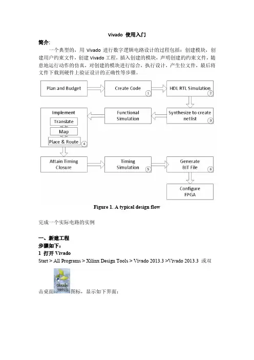
Vivado 使用入门简介:一个典型的,用Vivado进行数字逻辑电路设计的过程包括:创建模块,创建用户约束文件,创建Vivado工程,插入创建的模块,声明创建的约束文件,随意地运行动作的仿真,对创建的模块进行综合,执行设计,产生位文件,最后将文件下载到硬件上验证设计的正确性等步骤。
Figure 1. A typical design flow完成一个实际电路的实例一、新建工程步骤如下:1 打开VivadoStart > All Programs > Xilinx Design Tools > Vivado 2013.3 >Vivado 2013.3 或双击桌面图标,显示如下界面:“Creating New Project”:建立新工程导航,用于建立各种类型的工程。
“Open Project”:打开一个已有的工程。
“Open Example Project”:打开示例工程。
“Documentation and Tutorials”:文件夹和说明书。
可以打开Xilinx使用说明书和部分设计数据。
“User Guide”:打开Vivado用户指南。
“Quick Take Videos”:打开Xilinx视频说明书。
2 点击“Create New Project”,开始新建工程向导。
弹出下图点击“Next”,进入设置此次所建项目的名称对话框。
第一次实验前,请为本课程所有的项目新建一个文件夹,如“digital”,以后所有本课程相关项目均放在此文件夹下,在“project location”栏选择此文件夹。
接着,为本项目取名,如“tutorial01”,勾选“Create Project Subdirectory”,在当前目录下为本工程新建一个同工程名的子目录,保存工程所有数据文件。
注意:工程名称和存储路径中不能出现中文和空格,建议工程名称和路径名称都是以字母开头,由字母、数字、下划线来组成。
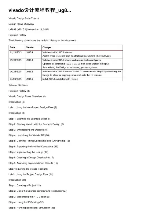
vivado设计流程教程_ug8... Vivado Design Suite TutorialDesign Flows OverviewUG888 (v2015.4) November 18, 2015Revision HistoryThe following table shows the revision history for this document.Table of ContentsRevision History (2)Vivado Design Flows Overview (4)Introduction (4)Lab 1: Using the Non-Project Design Flow (8)Introduction (8)Step 1: Examine the Example Script (8)Step 2: Starting Vivado with the Example Design (8)Step 3: Synthesizing the Design (10)Step 4: Launching the Vivado IDE (10)Step 5: Defining Timing Constraints and I/O Planning (12) Step 6: Exporting the Modified Constraints (15)Step 7: Implementing the Design (16)Step 8: Opening a Design Checkpoint (17)Step 9: Analyzing Implementation Results (17)Step 10: Exiting the Vivado Tool (20)Lab 2: Using the Project Design Flow (21)Introduction (21)Step 1: Creating a Project (21)Step 2: Using the Sources Window and Text Editor (27)Step 3: Elaborating the RTL Design (31)Step 4: Using the IP Catalog (32)Step 5: Running Behavioral Simulation (33)Step 6: Reviewing Design Run Settings (34)Step 7: Synthesizing and Implementing the Design (37)Step 8: Analyzing the Synthesized Design (38)Step 9: Analyzing the Implemented Design (41)Step 10: Generating a Bitstream file (43)Conclusion (45)Legal Notices (46)Please Read: Important Legal Notices (46)Vivado Design Flows OverviewIMPORTANT: This tutorial requires the use of the Kintex?-7 family of devices. You willneed to update your Vivado tools installation if you do not have this device family installed.Refer to the Vivado Design Suite User Guide: Release Notes, Installation, and Licensing(UG973) for more information on Adding Design Tools or Devices.IntroductionThis tutorial introduces the use models and design flows recommended for use with the Xilinx? Vivado?Integrated Design Environment (IDE). This tutorial describes the basic steps involved in taking a small example design from RTL to bitstream, using two different design flows as explained below. Both flows can take advantage of the Vivado IDE, or be run through batch Tcl scripts. The Vivado Tcl API provides considerable flexibility and power to help set up and run your designs, as well as perform analysis and debug.VIDEO:You can also learn more about the Vivado Design Suite design flows by viewing thequick take video at Vivado Design Flows.TRAINING: Xilinx provides training courses that can help you learn more about theconcepts presented in this document. Use these links to explore related courses:Vivado Introductory WorkshopVivado Design Suite Tool FlowEssentials of FPGA DesignWorking in Project Mode and Non-Project ModeSome users prefer the design tool for automatically managing their design flow process and design data, while others prefer to manage sources and process themselves. The Vivado Design Suite uses a project file () and directory structure to manage the design source files, store the results of different synthesis and implementation runs, and track the project status through the design flow. This automated management of the design data, process and status requires a project infrastructure. For this reason, Xilinx refers to this flow as the Project Mode.Other users prefer to run the FPGA design process more like a source file compilation, to simply compile the sources, implement the design, and report the results. This compilation style flow isreferred to as the Non-Project mode. The Vivado Design Suite easily accommodates both of these use models.Both of these flows utilize a project structure to compile and manage the design. The main distinctions are that Non-Project mode processes the entire design in memory. No files are written to disk. While Project mode creates and maintains a project directorystructure on disk to manage design sources, results, and project settings and status.The following provides a brief overview of Project mode and Non-Project mode. For a more complete description of these design modes, and the features and benefits of each, refer to this link in the Vivado Design Suite User Guide: Design Flows Overview (UG892).Non-Project ModeThis use model is for script-based users who do not want Vivado tools to manage their design data or track their design state. The Vivado tools simply read the various source files and compile the design through the entire flow in-memory. At any stage of the implementation process, you can generate a variety of reports, run design rule checks (DRCs), and write design checkpoints. Throughout the entire flow, you can open the design in-memory, or any saved design checkpoint, in the Vivado IDE for design analysis or netlist/constraint modification. Source files, however, are not available for modification in the IDE when running the Non-Project mode. It is also important to note that this mode does not enable project-based features such as source file and run management, cross-probing back to source files, design state reporting, etc. Essentially, each time a source file is updated on the disk; you must know about it and reload the design.There are no default reports or intermediate files created within the Non-Project mode. You must direct the creation of reports or design checkpoints with Tcl commands.Project ModeThis use model is for users who want the Vivado tools to manage the entire design process, including features like source file, constraint and results management, integrated IP design, and cross probing back to sources. In Project mode, the Vivado tools create a directory to manage the design source files, IP data, synthesis and implementation run results and related reports. The Vivado Design Suite manages and reports the status of the source files, configuration, and the state of the design. You can create and configure multiple runs to explore constraint or command options. In the Vivado IDE, you can cross-probe implementation results back to the RTL source files. You can also script the entire flow with Tcl commands, and open Vivado IDE as needed. Using Tcl CommandsThe Tcl commands and scripting approach vary depending on the design flow used. When using the Non-Project mode, the source files are loaded using read_verilog, read_vhdl, read_edif,read_ip, and read_xdc commands. The Vivado Design Suite creates an in-memory design database to pass to synthesis, simulation, and implementation. When using Project mode, you can use thecreate_project, add_files, import_files, and add_directories commands to create theproject infrastructure needed to manage source files and track design status. Replace the individual “atomic” commands,synth_design, opt_design, place_design, route_design, andwrite_bitstream in the Batch flow, with an all-inclusive command called launch_runs. The launch_runs command groups the atomic commands together with other commands to generate default reports and track the run status. The resulting Tcl run scripts for the Project mode are different from the Non-Project mode. This tutorial covers the Project mode and Non-Project mode, as well as the Vivado IDE.Many of the analysis features discussed in this tutorial are covered in more detail in other tutorials. Not every command or command option is represented here. To view the entire list of Tcl commands provided in the tools, consult the Vivado Design Suite Tcl Command Reference Guide (UG835).This tutorial contains two labs that can be performed independently.Lab 1: Using the Non-Project Design FlowWalk through a sample run script to implement the bft design.View various reports at each step.Review the vivado.log file.Write design checkpoints.Open the Vivado IDE after synthesis to review timing constraint definition and I/O planning and demonstrate methods to update constraints.Open the implemented Design Checkpoint to analyze timing, power, utilization and routing.Lab 2: Using the Project Based Design FlowCreate a new project.Walk through implementing the bft design using the Vivado IDE.View various reports at each step.Open the synthesized design and review timing constraint definition, I/O planning and design analysis.Open the implemented design to analyze timing, power, resource utilization, routing, and cross-probing.Tutorial Design DescriptionThe sample design used throughout this tutorial consists of a small design called bft. There are several VHDL and Verilog source files in the bft design, as well as a XDC constraints file.The design targets an xc7k70T device. A small design is used to allow the tutorial to be run with minimal hardware requirements and to enable timely completion of the tutorial, as well as to minimize the data size.Hardware and Software RequirementsThis tutorial requires that the 2015.3 Vivado Design Suite software release or later is installed. The following partial list describes the operating systems that the Vivado Design Suite supports on x86 and x86-64 processor architectures:See the Vivado Design Suite User Guide: Release Notes, Installation, and Licensing (UG973) for a complete list and description of the system and software requirements.Preparing the Tutorial Design FilesYou can find the files for this tutorial in the Vivado Design Suite examples directory at the following location:/Vivado//examples/Vivado_TutorialYou can also extract the provided ZIP file, at any time, to write the tutorial files to your local directory, or to restore the files to their starting condition.Extract the ZIP file contents from the software installation into any write-accessible location./Vivado//examples/Vivado_Tutorial.zipThe extracted Vivado_Tutorial directory is referred to as the in this Tutorial. Note: You will modify the tutorial design data while working through this tutorial. You should use a new copy of the original Vivado_Tutorial directory each time you start this tutorial. Lab 1: Using the Non-Project Design FlowIntroductionThis lab focuses on Non-Project mode and the associated Tcl commands.Step 1: Examine the Example Script1.Open the example script:/Vivado_Tutorial/create_bft_kintex7_batch.tcl, in a text editor and review the different steps.STEP#0: Define output directory location.STEP#1: Setup design sources and constraints.STEP#2: Run synthesis, report utilization and timing estimates, write checkpoint design.STEP#3: Run placement and logic optimization, report utilization and timingestimates, write checkpoint design.STEP#4: Run router, report actual utilization and timing, write checkpointdesign, run drc, write verilog and xdc out.STEP#5: Generate a bitstream.Notice that many of the Tcl commands are commented out. You will run them manually, one at a time.2.Leave the example script open, as you will copy and paste commands from it later in this tutorial. Step 2: Starting Vivado with the Example DesignOn Linux1.Change to the directory where the lab materials are stored:cd /Vivado_Tutorial/doc/0aad815a178884868762caaedd3383c4bb4cb489.html unch the Vivado Design Suite Tcl shell, and source a Tcl script to create the tutorial design:vivado -mode tcl -source create_bft_kintex7_batch.tclOn Windows/doc/0aad815a178884868762caaedd3383c4bb4cb489.html unch the Vivado Design Suite Tcl shell: Start > All Programs > Xilinx Design Tools > Vivado 2015.x >Vivado 2015.x Tcl ShellNote: Your Vivado Design Suite installation may be called something other than Xilinx Design Tools on the Start menu.2.In the Tcl shell, change to the directory where the lab materials are stored:Vivado% cd /Vivado_Tutorial3.Source a Tcl script to create the tutorial design:Vivado% source create_bft_kintex7_batch.tclAfter the sourced script has completed, the Vivado Design Suite Tcl shell, hereafter called the Tcl shell, displays the Tcl prompt: Vivado%Figure 1: Start Vivado and Source Tcl ScriptYou can enter additional Tcl commands from the Tcl prompt.Step 3: Synthesizing the Design1.Copy and paste the synth_design command from the create_bft_kintex7_batch.tclscript into the Tcl shell and wait for synthesis to complete. You can paste into the Tcl shell using the popup menu, by clicking the right mouse button.synth_design -top bftNote:The command in the example script is a comment. Do not copy the leading ‘#’ character, or your command will also be interpreted as a comment.2.Examine the synthesis report as it scrolls by.3.When the Vivado Tcl prompt has returned, copy and paste the write_checkpoint,report_timing_summary, report_power, report_clock_interaction, andreport_high_fanout_nets commands that follow synthesis.write_checkpoint -force $outputDir/post_synthreport_timing_summary -file $outputDir/post_synth_timing_summary.rptreport_power -file $outputDir/post_synth_power.rptreport_clock_interaction -delay_type min_max -file \$outputDir/post_synth_clock_interaction.rptreport_high_fanout_nets –fanout_greater_than 200 -max_nets 50 -file \$outputDir/post_synth_high_fanout_nets.rpt4.Open another window to look at the files created in the output directory. On Windows, it may beeasier to use the file browser./Vivado_Tutorial/Tutorial_Created_Data/bft_output/doc/0aad815a178884868762caaedd3383c4bb4cb489.html e a text editor to open the various report (*.rpt) files that were created.Step 4: Launching the Vivado IDEEven though a Vivado project has not been created on disk, the in memory design is available in the tool, so from the Tcl shell you can open the Vivado IDE to view the design.Non-Project mode enables the use of the Vivado IDE at various stages of the design process. The current netlist and constraints are loaded into memory in the IDE, enabling analysis and modification. Any changes to the logic or the constraints are live in memory and are passed to the downstream tools. This is quite a different concept than with the ISE tools that require saving and reloading files.Open the IDE using the start_gui command.Vivado% start_guiThe Vivado IDE provides design visualization and exploration capabilities for your use. From the Vivado IDE, you can perform further analysis and constraint manipulation on the design.Figure 2: Vivado IDE - Non-Project Modecommand. If you use the File > Exit command from the Vivado IDE, you will completelyexit the Vivado tool.Since the design does not have a project in Non-Project mode, the Vivado IDE does not enable source file or run management. You are effectively analyzing the current in memory design. The Vivado FlowNavigator and other project based commands are also not available in Non-Project mode.Step 5: Defining Timing Constraints and I/O PlanningYou must often define timing and physical constraints for the design prior to implementation. The Vivado tools let you load constraints from constraints file(s), or enter constraints interactively using the IDE.Defining Timing Constraints1. Open the Timing Constraints window: Window > Timing Constraints, as shown in the followingfigure:Figure 3: Define Timing ConstraintsA tree view of the different types of constraints displays on the left side of the Timing Constraintswindow. This is a menu of timing constraints that can be quickly defined.Notice the two clock constraints, wbClk and bftClk, displayed in the Timing Constraintspreadsheet on the right side of the Timing Constraints window. The values of currently defined constraints can be modified by directly editing them in the spreadsheet.2.In the left hand tree view of the Timing Constraints window,double-click Create Clock under theClocks category, as shown in Figure 3.Note: Expand the Clocks category if needed by clicking the +.The Create Clock wizard opens, as shown in the following figure, to help you define clockconstraints. Notice the Tcl Command line on the bottom displays the XDC command that will be executed.Do not create or modify any timing constraints at this time.Figure 4: Create Clock Dialog Box3.Click Cancel.4.Close the Timing Constraints window by clicking the X in the window tab.The Vivado Design Suite offers a variety of features for design analysis and constraint assignment.Other tutorials cover these features in detail, and they are only mentioned here. Feel free toexamine some of the features under the Tools menu.matlI/O PlanningVivado has a comprehensive set of capabilities for performing and validating I/O pin assignments. These are covered in greater detail in the I/O Planning Tutorial.1.Open the I/O Planning view layout by selecting I/O Planning from the Layout Selector pull down,as shown in Figure 5.2.Make the Package window the active view if it is not active.Note: If the Package window is not open, you can open it using the Windows > Packagecommand from the main menu.Figure 5: Open I/O Planning View Layout3.In the Package window, double-click to select a placed I/O Port, shown asan orange block inside a package pin.4.Drag the selected I/O Port onto another pin site in the same I/O bank.5.Examine the I/O Ports window, look at the port name and package pinsite columns.6.Examine the data displayed in the I/O Port Properties window. Click eachof the tabs at the bottom of the window.7.Remember the port name and site of the port you moved.If necessary, write them down. You will look for the LOC constraint of the placed port in the XDC file after implementation.Step 6: Exporting the Modified ConstraintsModified constraints can be output for later use. You can also save design checkpoints that include the latest changes. You will explore design checkpoints later in this tutorial.IMPORTANT: The Vivado Design Suite does not support NCF/UCF constraints. Youshould migrate existing UCF constraints to XDC format. Refer to the ISE to VivadoDesign Suite Migration Guide (UG911) for more information./doc/0aad815a178884868762caaedd3383c4bb4cb489.html e the Export Constraints command to output a modified XDC constraints file with the new I/OLOC constraint value.File > Export > Export ConstraintsThe Export Constraints dialog box opens to let you specify a file name to create, as shown in the following figure.Figure 6: Export Constraints2.Enter a name and location for the file and click OK.Notice the checkbox for Include unconstrained placement locations. When this is enabled, LOC constraints of all placed cells are exported, rather than of only fixed cells. For a more detailed description of fixed versus unfixed cells, refer to this link in the Vivado Design Suite User Guide: Using Constraints (UG903)./doc/0aad815a178884868762caaedd3383c4bb4cb489.html e the File > Open File command to open the constraints file in the Text Editor.4.Browse to select the newly exported constraints file and click OK.5.Notice the file reflects the I/O Port placement change you made earlier.You can open any ASCII file in the Text Editor. This is helpful for editing Tcl scripts and constraints files, and viewing reports. The Text Editor is context sensitive, and highlights keywords andcomments when displaying file types such as Verilog, VHDL, XDC, and Tcl.6.Select the Tcl Console tab at the bottom of the IDE, and enter the stop_gui command.The Vivado IDE closes, and you are returned to the Tcl prompt in the Tcl shell.Step 7: Implementing the Design1.Open the create_bft_kintex7_batch.tcl script, or bring the script window to the front.2.Individually copy and paste the Tcl commands in the script, in order from opt_design towrite_bitstream:opt_designplace_designphys_opt_designwrite_checkpoint -force $outputDir/post_placereport_timing_summary -file $outputDir/post_place_timing_summary.rptroute_designwrite_checkpoint -force $outputDir/post_routereport_timing_summary -file $outputDir/post_route_timing_summary.rptreport_timing -sort_by group -max_paths 100 -path_type summary –file \$outputDir/post_route_timing.rptreport_clock_utilization -file $outputDir/clock_util.rptreport_utilization -file $outputDir/post_route_util.rptreport_power -file $outputDir/post_route_power.rptreport_drc -file $outputDir/post_imp_drc.rptwrite_verilog -force $outputDir/bft_impl_netlist.vwrite_xdc -no_fixed_only -force $outputDir/bft_impl.xdcwrite_bitstream -force $outputDir/bft.bit3.Examine each command and notice the various messages produced as the commands are run.4.Close the text editor displaying the create_bft_kintex7_batch.tcl script.5.Examine the files created in the output directory./Vivado_Tutorial/Tutorial_Created_Data/bft_output/doc/0aad815a178884868762caaedd3383c4bb4cb489.html e a text editor to open the various report (*.rpt) files that were created.7.Open the bft_impl.xdc file.8.Validate that the design has been implemented with the I/O Port constraint that you modifiedearlier.Step 8: Opening a Design CheckpointThe Vivado IDE can open any saved design checkpoint. This snapshot of the design can be opened in the Vivado IDE or Tcl shell for synthesis, implementation, and analysis.1.Open the Vivado IDE again: start_guiThis loads the active design in-memory into the IDE.You will now load the implemented design checkpoint, closing the current in-memory design. 2.Open the implemented checkpoint.Use File > Open Checkpoint and browse to select the checkpoint file:/Vivado_Tutorial/Tutorial_Created_Data/bft_output/post_route.dcp3.If prompted, select Close Without Saving to close the current in-memory design.Now you can use the visualization and analysis capabilities of the IDE, working from a placed and routed design checkpoint. Step 9: Analyzing Implementation ResultsVivado has an extensive set of features to examine the design and device data from a number of perspectives. You can generate standard reports for power, timing, utilization, clocks, etc. With the Tcl API, the custom reporting capabilities in the Vivado tools are extensive.1.Click on the Device window tab to bring it front to the screen.2.Run the report_timing_summary command to analyze timing data.Tools > Timing > Report Timing Summary3.In the Report Timing Summary dialog, click OK to accept the default run options.Examine the information available in the Timing Summary window. Select the various categories from the tree on the left side of the Timing Summary window and examine the data displayed. 4.Now run the report_timing command to perform timing analysis Tools > Timing > Report Timing5.In the Report Timing dialog, click OK to accept the default run options.6.Collapse the bftClk tree in the Timing Checks – Setup window.7.Select the first path listed under the wbClk in the Setup area.8.Maximize or float the Path Properties window to look at the path details.Figure 7: Float the Path Properties Window9.Restore the Path Properties window by clicking the Restore button, or the Dock button, in thewindow banner.10.In the Timing – Report Timing window, right-click to open the popup menu and select theSchematic command to open a Schematic window for the selected path.Note: Alternatively, you can press the F4 function key to open the Schematic window.11.Double-click on a schematic object, such as on a cell, pin, or wire, to expand the schematicconnections and traverse the design hierarchy.12.Close the Schematic window, or click the Device window tab to bring it to the front.13.In the Device window, check to ensure that the Routing Resources button is enabled to displaythe detailed device routing.Notice the Device window displays and highlights the routing for the selected path.Figure 8: Displaying the Device Routing14.Select the Auto Fit Selection button in the Device window toolbar menu to enable the Vivado IDE to automatically zoom into selected objects.15.Select some additional paths from the Timing results window.16.Examine the routing for the selected paths in the Device window.17.Expand the Tools main menu and examine the available analysis features under the different sub-menus such as Timing and Report.18.Run some of the available analysis commands: Report Power, Report Clock Interaction, Report Clock Networks, Report Utilization, etc.Many of these Design Analysis features are covered in other Vivado tutorials.。
Vivado使用方法Vivado是一款全面的FPGA设计工具套件,主要用于ASIC、FPGA硬件设计和开发。
该工具套件提供了基于IP管理、综合、实现、建模等组件,同时还有用于调试和分析的工具。
Vivado支持一系列设计语言,包括Verilog、VHDL、SystemVerilog等。
这里介绍一下Vivado的使用方法,包括工程创建、IP核添加、约束文件添加、综合和实现。
一. 工程创建和添加文件在电脑上进入Vivado软件,然后选择“Create Project”,在弹出的窗口中设置工程的名字和路径等相关信息,选择创建工程。
在工程创建完成后,需要添加文件。
这些文件包括hdl文件、约束文件、仿真模型、模块文档等。
在Vivado中添加文件的方式如下:点击菜单栏“File → Add Sources”,选择要添加的文件类型对应的选项。
例如要添加一个Verilog文件,选择“Add or create design sources”,然后选择“Add Files...”,并选择相应的文件。
二. IP核添加Vivado提供了大量的IP核,可以帮助设计师快速构建基础电路。
可以通过以下步骤将IP核添加到工程中:点击菜单栏“Tools → Create and Package IP”,弹出“Create and Package New IP”对话框。
按照提示完成IP核的创建和封装,并选择“Add IP...”将IP核添加到工程中。
三. 约束文件添加在进行综合和实现之前,需要先添加一个约束文件。
这些约束文件用于描述设计中的时序和约束条件,并将这些信息传递给Vivado工具进行综合和实现。
四. 综合综合是将原理图转换成可编程逻辑单元的过程,通常用来验证设计中的逻辑功能。
在Vivado中进行综合,可以通过以下方法:点击菜单栏“Flow Navigator → Run Synthesis”选项卡,然后点击“Run Synthesis”按钮。
vivado synthesis implementation 流程Vivado是一款用于FPGA设计的综合与实现工具,它是由Xilinx公司开发的,提供了全面的设计和验证环境。
本文将分步介绍Vivado的综合与实现流程,以帮助读者更好地了解如何使用Vivado进行FPGA设计。
第一步:创建工程首先,在Vivado中创建一个新的工程。
选择“Create New Project”并填写工程名称、路径等信息。
然后,选择工程类型(例如RTL设计),以及目标设备(例如Xilinx的Artix-7系列)。
第二步:添加设计文件在创建工程后,需要添加设计文件。
这些文件包括RTL源代码文件、约束文件等。
通过选择“Add Sources”按钮,可以将设计文件添加到工程中。
第三步:约束与设置在添加设计文件后,需要为设计添加约束。
约束文件为Vivado提供了关于时钟、时序要求等重要信息。
通过选择“Add Constraints”按钮,可以添加约束文件。
此外,还可以进行一些设置,例如选择时钟频率、时序约束等。
第四步:运行综合在完成约束与设置后,可以运行综合工具对设计进行综合。
综合将RTL代码转换为门级网表,并进行一系列的优化以实现设计的功能。
第五步:查看综合报告在综合完成后,可以查看综合报告。
综合报告提供了关于设计资源使用情况、时序分析等重要信息。
通过查看综合报告,可以评估设计的性能、资源占用等情况。
第六步:运行实现在确认综合结果无误后,可以运行实现工具对设计进行实现。
实现工具将门级网表映射到目标FPGA设备的特定元件中,并进行布局和布线等过程。
第七步:查看实现报告在实现完成后,可以查看实现报告。
实现报告提供了关于布局、布线、时序分析等重要信息。
通过查看实现报告,可以评估设计的性能、资源占用等情况。
第八步:生成比特流文件在实现成功后,可以生成比特流文件。
比特流文件包含了设计在目标FPGA 设备中的配置信息。
这些信息将在FPGA启动时加载到其配置存储器中,以实现设计的功能。

vivado设计流程
Vivado设计流程主要包括以下几步:
1. 创建新工程:使用Vivado工具打开,并创建一个新的工程。
2. 添加设计文件:将设计文件添加到工程中,可以选择VHDL、Verilog、IP等。
3. IP集成:如果需要使用第三方IP,可以将其加入工程中。
4. 约束文件:创建约束文件并将其添加到工程中,约束文件描述了设计的时钟、时序等要求。
5. 综合:进行逻辑综合工作,将设计代码转换为等效的门级网表。
6. 实现:将综合结果映射到目标FPGA器件中,包括时序分析、布局和布线。
7. 生成比特流:生成比特流文件(bitstream),用于配置FPGA器件。
8. 时序分析:对设计进行时序分析,确保满足时序约束。
9. 产生报告:生成综合、实现、时序分析等相关的报告。
10. 下载到目标设备:将生成的比特流文件下载到FPGA器件
中进行验证和调试。
11. 调试和优化:通过观察设计在FPGA器件上的实际运行情况,进行调试和性能优化。
12. 生成最终产品:在验证和优化完成后,生成最终产品,如FPGA原型或嵌入式系统。
以上是Vivado设计流程的一般步骤,具体的流程可能会因设计的复杂性和需求的不同而有所区别。
VIVADO教程Vivado是美国赛灵思公司(Xilinx)推出的一款可视化集成环境(IDE),用于FPGA(现场可编程门阵列)和SoC(系统级芯片)的设计和开发。
它提供了一个完整的设计流程,从设计输入到最终的实现和验证,为FPGA和SoC设计师提供了强大的工具和功能。
下面是一个简要的Vivado教程,介绍了其基本功能和使用方法。
第一步:安装Vivado第二步:创建新项目在Vivado中,您需要创建一个新的项目来开始您的设计。
选择“File”菜单中的“New Project”,然后按照指示进行操作。
在创建项目的过程中,您需要选择项目的目录、名称和基本设置,以及FPGA或SoC的型号。
第三步:设计输入在新项目中,您可以添加设计文件、约束文件和仿真文件。
设计文件可以是VHDL或Verilog代码,约束文件用于设置时序和引脚约束,而仿真文件用于验证设计。
第四步:约束设置第五步:综合和实现在设计输入和约束设置完成后,您可以对设计进行综合和实现。
综合将设计转化为逻辑门级别,实现则将逻辑门级别映射到FPGA或SoC中的具体资源和连接。
这个过程需要一定的时间,取决于设计的复杂性和目标设备的类型。
第六步:比特流生成第七步:验证在比特流生成之后,您可以对设计进行验证。
Vivado提供了一些强大的仿真工具,可以用于验证设计的功能和性能。
您可以通过添加测试向量来进行仿真,并检查设计的输出是否正确。
第八步:生成硬件描述文件在验证之后,您可以生成硬件描述文件,以便与软件进行集成。
硬件描述文件可以是RTL级别的VHDL或Verilog代码,也可以是系统级别的IP核。
第九步:导出设计在项目开发完成后,您可以将设计导出到其他工具中进行后续处理。
Vivado支持将设计导出为EDIF、NGC、VHDL、Verilog等格式。
您可以根据需要选择最适合的格式。
总结:以上是一个简要的Vivado教程,介绍了其基本功能和使用方法。
Vivado是一个功能强大的FPGA和SoC开发工具,提供了完整的设计流程和一系列的工具和功能。

vivado 使用手册Vivado 是一款由 Xilinx 公司开发的集成电路设计工具,广泛应用于 FPGA(现场可编程门阵列)的开发和设计过程中。
该使用手册将帮助您了解 Vivado 工具的基本功能和使用方法,使您能够更加高效地进行电路设计和验证。
首先,了解 Vivado 的基本概念是非常重要的。
Vivado 工具主要由两个部分组成:Vivado 设计套件和 Vivado 高级综合(HLS)。
Vivado 设计套件是一个全面的集成电路设计解决方案,包括设计、调试和验证等多个环节。
而 Vivado HLS 则是一种高级综合工具,可将 C/C++ 代码转换为可在 FPGA 上实现的硬件描述语言。
在开始使用 Vivado 进行设计时,您需要创建一个项目。
项目由设计文件、约束文件和其他相关文件组成。
设计文件可以使用 Verilog、VHDL 或其他硬件描述语言编写,约束文件用于指定电路的时序约束和板级约束等信息。
通过 Vivado 的GUI(图形用户界面)或 TCL(工具命令语言)进行项目管理和配置。
Vivado 提供了丰富的功能和工具,可帮助您进行电路设计、仿真和验证。
您可以使用自动布局布线(Auto Place and Route)工具自动生成电路的物理布局和连线。
借助 Vivado 的时序分析工具,您可以分析电路的时序约束和时钟域,以确保电路的性能和稳定性。
此外,还可以使用仿真工具验证电路的功能和正确性,并进行系统级调试和验证。
Vivado 还支持 IP(知识产权)核的使用。
IP 核是预先设计好的可重用电路模块,可以直接用于您的设计中,加快设计时间和减少工作量。
Vivado 拥有丰富的IP 核库,包含各种不同的功能模块,如存储器、接口、调制解调器等。
您可以使用 Vivado 的 IP 目录来浏览和添加 IP 核,也可以自定义开发您自己的 IP 核。
最后,在完成设计后,您可以使用 Vivado 工具将设计文件进行编译,并将生成的 Bitstream 文件下载到 FPGA 板卡上进行硬件实现和验证。
VIVADO设计工具使用流程Vivado是赛灵思(Xilinx)公司推出的一款集成电路设计工具套件,用于设计、仿真和综合FPGA和SoC。
它提供了一种全面的设计工作流程,以帮助电子工程师开发复杂的硬件系统。
下面将详细介绍Vivado的使用流程。
1.项目设置:首先,打开Vivado并选择“Create Project”选项,然后选择一个文件夹用于存储项目文件。
在项目设置向导中,设置项目名称、存储位置和目标设备等信息。
还可以选择添加已有的设计文件,并选择一个默认的综合目标以及仿真目标。
2.创建设计:在项目设置完成后,可以开始创建设计。
设计可以通过各种方式创建,包括使用Vivado IP(Intellectual Property)库、设计向导、手动编写代码等。
根据设计需求,选择适当的方式创建设计。
3.添加制约条件:在设计中,制约条件(Constraints)对于硬件系统的正确功能起着至关重要的作用。
制约条件定义了信号的时序要求、引脚约束、时钟频率等。
通过添加约束文件,可以为设计添加相关的制约条件。
4.IP集成:在设计中,可以使用IP核来简化设计和提高效率。
Vivado提供了广泛的IP核库,可以选择合适的IP核并集成到设计中。
通过IP集成,可以重用现有的功能模块,并快速构建复杂的硬件系统。
5.综合:在设计完成后,需要对设计进行综合,将设计转换为逻辑门级网表表示。
选择“Run Synthesis”选项,Vivado将自动综合设计,并生成综合结果报告。
综合报告可以用于评估设计的资源利用率、时序要求是否满足等。
6.时序分析:在综合完成后,可以进行时序分析,以确保设计满足时序要求。
通过选择“Run Implementation”选项,Vivado将自动进行时序分析,并生成时序报告。
时序报告可以用于评估设计的时序性能,发现和解决时序约束的问题。
7.实现:8.仿真:在设计生成位文件后,可以进行仿真验证,以确保设计的正确性和功能性。
弹出主菜单界面,点击create new project这是介绍界面,next~添加好工程名,和工程位置,next~选择rtl Project,选择板卡型号,我这里使用的是A-7系列的basys3,用户根据自己的板卡型号自定义,next~这一面是总结,finish~左边这一栏,我们用到哪里解释哪里,首先,点击add source 添加verilog HDL文件选择新建一个设计文件,next~左边是添加已有的文件,右边是新建一个verilog HDL文件,我们前面没有文件,所以选择新建一个新的文件上面是文件类型,我用的是verilog,添加文件名,我这里用的是流水灯,文件名为led_water添加成功,点击finish点击OKYes双击这个文件,打开编写这是一个流水灯工程编写完成后,点击如图所示可以,编译文件,也可查看工程的RTL图这是生成的RTL图,双击如图所示部分可以将窗口放大。
原理图出来后,说明该工程没有语法错误,然后再次add source,选择add or create simulation source添加测试文件,同样选择新建一个文件Yes找到到tb_led_water文件双击打开编写测试文件点击run simulation 点击 run behavioral simulation 进行仿真12reg[25:0] cnt;//设定一个26位的计数器3parameter TIME = 26'd;4 //parameter TIME = 26'd500;//just test注意,仿真前把测试文件改小一点,不然跑的太慢,点击run-all让流水灯跑起来,可以看到流水灯的数值在变化,说明设置正确。
然后要做的是下板子仿真点击add source 添加约束文件,add constraints新建一个引脚约束文件,OK点击新建好的文件,将约束文件内容复制进去,最后点击大综合,对工程进行综合,综合完成后就可以下板子了。
Vivado设计流程以一个简单的16位拨码开关的读和16位LED灯的输出电路为例,利用Verilog HDL语言,在Vivado中创建简单的16位拨码开关的输入和16位LED灯的输出电路,将设计下载的Xilinx 大学计划ARTIX-7平台。
一、新建工程1、打开Vivado,然后点击创建一个新项目(或者在菜单栏选择File->NewProject…),然后点next。
2、输入工程名称、选择工程存储路径,并勾选Create projectsubdirectory选项,为工程在指定存储路径下建立独立的文件夹。
设置完成后,点击Next。
最后,如图,整个项目将在D:/FPGAprojects/myproject中。
注意:工程名称和存储路径中不能出现中文和空格,建议工程名称以字母、数字、下划线来组成。
3、选择RTL Project一项,并勾选Do not specify sources at this time,勾选该选项是为了跳过在新建工程的过程中添加设计源文件。
点击Next。
4、根据使用的FPGA开发平台,选择对应的FPGA目标器件。
Nexys4开发板请选择Artix-7 XC7A100TCSG324-1的器件,即Family和Subfamily均为Artix-7,封装形式(Package)为CSG324,速度等级(Speed grade)为-1,温度等级(Temp Grade)为C)。
点击Next。
5、确认相关信息与设计所用的的FPGA器件信息是否一致,一致请点击Finish,不一致,请返回上一步修改。
6、得到如下的空白Vivado工程界面,完成空白工程新建。
二、设计文件输入1、点击Flow Navigator下的Project Manager->Add Sources或中间Sources中的对话框打开设计文件导入添加对话框。
2、选择第二项Add or Create Design Sources,用来添加或新建Verilog或VHDL源文件,点击Next。
VIVADO教程Vivado是一种先进的、全面的FPGA设计和开发软件,由Xilinx公司开发。
它提供了设计、验证和实现FPGA和SoC解决方案的全套工具和功能。
本教程将介绍如何使用Vivado进行FPGA设计,包括项目创建、代码编写、仿真和实现等步骤。
1.项目创建在打开Vivado软件后,选择"Create New Project"来创建一个新项目。
按照向导的提示,选择项目名称、存储位置和目标设备等信息。
然后选择所需的工程类型,如RTL项目或IP集成项目。
最后选择工程源文件和约束文件,并点击"Finish"完成项目创建。
2.代码编写在Vivado中,可以使用多种语言编写FPGA设计代码,包括Verilog、VHDL和SystemVerilog等。
创建一个新文件,并将代码粘贴到文件中。
确保代码语法正确,并根据需要修改参数和端口定义。
3.模块综合在完成代码编写后,可以进行模块综合。
在Vivado中,选择"Flow"->"Run Synthesis"来对代码进行综合。
模块综合是将高级硬件描述语言(HDL)代码转换为门级网表的过程。
综合过程将代码优化并生成可实现的网表电路。
4.约束设置在进行设计实现之前,需要定义一些约束条件,以确保设计能够在FPGA上正确运行。
通过约束文件,可以指定时钟频率、I/O电平、时序要求等。
在Vivado中,选择"Design"->"Constraints"来添加约束文件,并根据需要定义约束。
5.仿真在进行设计实现之前,可以使用仿真工具来验证设计的正确性。
在Vivado中,选择"Flow"->"Run Simulation"来打开仿真工具。
在仿真工具中,可以加载测试向量并检查设计的输出。
如果仿真结果与预期一致,说明设计存在问题。
Vivado设计流程以一个简单的16位拨码开关的读和16位LED灯的输出电路为例,利用Verilog HDL语言,在Vivado中创建简单的16位拨码开关的输入和16位LED灯的输出电路,将设计下载的Xilinx 大学计划ARTIX-7平台。
一、新建工程1、打开Vivado,然后点击创建一个新项目(或者在菜单栏选择File->NewProject…),然后点next。
2、输入工程名称、选择工程存储路径,并勾选Create projectsubdirectory选项,为工程在指定存储路径下建立独立的文件夹。
设置完成后,点击Next。
最后,如图,整个项目将在D:/FPGAprojects/myproject中。
注意:工程名称和存储路径中不能出现中文和空格,建议工程名称以字母、数字、下划线来组成。
3、选择RTL Project一项,并勾选Do not specify sources at this time,勾选该选项是为了跳过在新建工程的过程中添加设计源文件。
点击Next。
4、根据使用的FPGA开发平台,选择对应的FPGA目标器件。
Nexys4开发板请选择Artix-7 XC7A100TCSG324-1的器件,即Family和Subfamily均为Artix-7,封装形式(Package)为CSG324,速度等级(Speed grade)为-1,温度等级(Temp Grade)为C)。
点击Next。
5、确认相关信息与设计所用的的FPGA器件信息是否一致,一致请点击Finish,不一致,请返回上一步修改。
6、得到如下的空白Vivado工程界面,完成空白工程新建。
二、设计文件输入1、点击Flow Navigator下的Project Manager->Add Sources或中间Sources中的对话框打开设计文件导入添加对话框。
2、选择第二项Add or Create Design Sources,用来添加或新建Verilog或VHDL源文件,点击Next。