AD9850模块使用手册
- 格式:pdf
- 大小:881.85 KB
- 文档页数:2
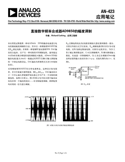
SET GNDGND+1.1VOne Technology Way • P.O. Box 9106 • Norwood, MA 02062-9106 • 781/329-4700 • World Wide Web Site: Rev. A | Page 1 of 2AN-423应用笔记R SET 引脚处的电压为(内部)控制放大器反馈环路的一部分,不得以外部方式予以更改。
R SET 调制电路(图2)以Q1为可变电阻,以R2为固定限流电阻,以防Q1过度开启。
当Q1工作于截止频率附近时,C1可以抑制噪声。
R1则可降低输入阻抗,从而进一步抑制噪声。
Q1上为完全调制AD9850输出所必需的输入电压约为1.5 v p-p ,直流失调约为2.3 v ,见图4。
直接数字频率合成器AD9850的幅度调制作者:Richard Cushing ,应用工程师本应用笔记将提供一种对AD9850 DDS 的输出电流进行电压控制或幅度调制的方法,其中以一种增强型MOSFET 取代R SET 固定电阻;并利用一种宽频RF 变压器将DDS DAC 输出结合起来,以产生一种对称的AM 调制包络。
速率超过50 kHz 时实现合理线性度的调制是可能的。
AD9850 DDS 的输出电流(最大20mA)一般通过从RSET(引脚12)输入到接地的一个固定电阻设定。
DAC 输出为单极性且互补(180度相位差)。
采用增强型MOSFET 符合单电源理念。
这种设计较为简单,并可尽量减少器件数量。
将I OUT 和I OUTB DAC 输出结合于一个中心抽头型宽频RF 变压器之中可产生一个对称的调制包络,如图1(A)所示。
图1(B)所示为不结合两个输出而仅仅采用一个输出的效应——非对称幅度调制。
两种配置均采用同一信号进行调制。
图2. R SET 改变图1. 对称(A)和非对称(B)幅度调制包络To I OUT OUTB PIN 20*MINI-CIRCUITS BROADBAND RF TRANSFORMERGNDGNDGNDGNDGND GNDAN-423Rev. A | Page 2 of 2©2011 Analog Devices, Inc. All rights reserved. Trademarks and registered trademarks are the property of their respective owners. 下面的图4展示了10 kHz 调制包络及其至Q1栅极的相关输入信号。
AD9850/9851DDS电路使用说明书江苏省无线电运动协会2007年3月9850/9851DDS电路简介AD9850/9851DDS电路是专为业余无线电电台设计的,它提供本机振荡信号和波段控制信号,特别适合做自制电台的本振源及老电台改造。
本电路使用有背光1602型通用液晶显示器,显示接收频率及工作模式。
电路大部分元器件为贴片封装,体积小,便于安装(PCB尺寸:36*93mm)。
在满足基本应用的条件下尽量简化设计,以提高性价比。
本电路可以使用AD9850(时钟100MHz)或AD9851(时钟20MHz)芯片,由用户设置。
中频频率可以由用户任意设置。
波段控制输出可以选择4波段或9波段,由用户设置。
所有设置均由软件实现并保存在芯片内。
关机前的工作频率将被保存,下次开机将工作在这个频率。
为简化电路,10MHz以下设计为高本振、10MHz以上为低本振,这样只要一个插入载频即可以完成对10MHz以下的LSB解调和10MHz以上的USB解调。
当然也可以用两个插入载频实现任意频率的上下边带解调。
主要功能如下:1.频率范围:0.1-30MHz2.频率分辨率:10Hz3.频率步进:10Hz、100Hz、1KHz、10KHz、100KHz、1MHz4.输出电平:约5dBm5.存储频点:20个存储频点可由用户任意设置。
6.显示模式:USB、LSB、CW、AM、FM7.接收频率微调:具有加减80KHz的接收频率微调功能。
8.收发转换:两种发信方式:普通方式和CW方式。
9.电源:电压8-12V DC,电流约180mA(背光打开),110mA(背光关闭)。
其他功能:1.频率校正:对DDS芯片的基准频率误差可通过软件设置校正。
2.边带切换:10MHz以下为LSB、10MHz以上为USB,自动切换。
CW发信方式是利用了DDS的特点而特别设计的,如果选择这种方式,则发信时DDS将直接输出所需的频率而不需要任何频率变换,简化了发信电路。
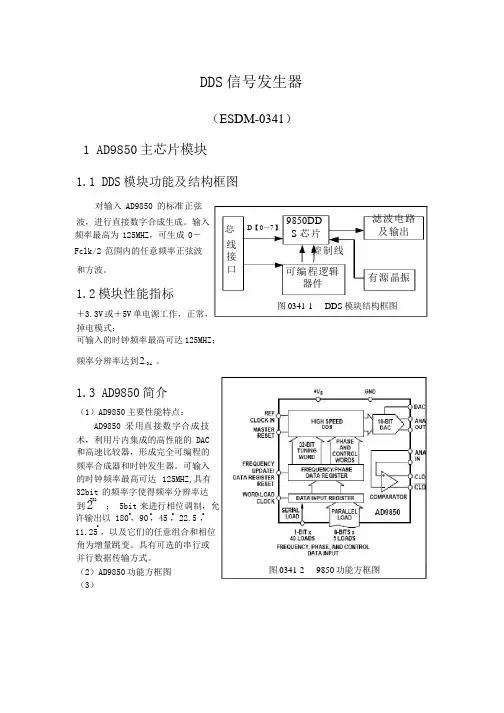
基于AD9850的信号发生器设计摘要介绍ADI 公司出品的AD9850 芯片,给出芯片的引脚图和功能。
并以单片机AT89S52 为控制核心设计了一个串行控制方式的正弦信号发生器的可行性方案,给出了单片机AT89S52 与AD9850 连接电路图和调试通过的源程序以供参考。
直接数字合成(DDS)是一种重要的频率合成技术,具有分辨率高、频率变换快等优点,在雷达及通讯等领域有着广泛的应用前景。
系统采用AD9850为频率合成器,以单片机为进程控制和任务调度的核心,设计了一个信号发生器。
实现了输出频率在10Hz~1MHz围可调,输出信号频率稳定度优于10-3的正弦波、方波和三角波信号。
正弦波信号的电压峰峰值Vopp能在0~5V围步进调节,步进间隔达0.1v,所有输出信号无明显失真,且带负载能力强。
该电路设计方案正确可行,频率容易控制,操作简单灵活,且具有广阔的应用前景。
关键词:信号发生器;直接数字频率合成;AD9850芯片;AT89S52单片机AbstractOn the basis of direct digital synthesis(DDS)principle, a signal generator was designed , using AT89S52 single chip machine as control device and adopting AD9850 type DDS device .Hardware design parameters were given .The system can output sine wave ,square wave with wide frequency stability and good waveform .The signal generator has stronger market competitiveness , with wide development prospect ,in frequency modulation technology and radio communication technology fields.Key words: signal generator ;direct digital synthsis;AD9850;AT89S52目录第一章绪论 (1)1.1背景 (1)1.2问题的提出 (2)1.3论证方案 (2)1.4总体设计框图 (3)第二章 DDS技术产生信号的基本原理 (5)2.1DDS简介 (5)2.2频率预置与调节电路 (5)2.3累加器 (6)2.4控制相位的加法器 (6)2.5控制波形的加法器 (6)2.6波形存储器 (6)2.7D/A转换器 (7)2.8低通滤波器 (7)2.9数字波形合成的理论分析 (8)第三章芯片的简介 (9)3.1AD9850结构与性能 (9)3.2AD9850的控制字与控制时序 (11)3.3 AT89S52结构与性能 (12)3.4 24C02结构与性能 (15)3.5MAX232的结构与性能 (16)3.6RT1602结构与性能 (17)第四章主要硬件的总体设计 (19)4.1AD9850与单片机的接口电路 (19)4.2 LCD与单片机的连接 (20)第五章软件部分设计 (21)第六章用到的数学原理 (24)6.1数学原理 (24)6.2算法比较和选择 (26)6.2.1采样回放法 (26)6.2.2查表法 (27)6.2.3泰勒级数展开法 (27)6.2.4数字正弦振荡器法 (27)6.2.5递推数列法 (28)第七章电路原理图的绘制 (31)7.1一般步骤 (31)7.2原理图的绘制 (31)结束语 (32)致 (33)第一章绪论1.1背景在电子技术领域中,也就是所谓的信号源号源有很多种,包括正弦波信号源、函数发生器、脉冲发生器、扫描发生器、任意波形发生器、合成的信号源等,经常要用一些信号作为测量基准信号或输入信号。
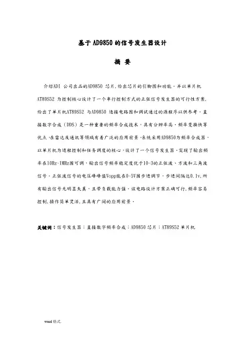
一、原理图
二、模块说明
1、
注意实物与原理图的对应关系,电路板上也做了功能标识。
2、
使用非常简单,仅仅使用主接口,即能完成全部工作。
3、
主接口红色部分(即P1-1,P1-2)为外接电源。
1引脚为+5V, 2引脚为地,接反会烧毁芯片。
注意外接电源需要纯净,否则,影响正弦信号高频特性。
4、
主接口粉色部分(即P1-3,P1-4,P1-5)为单片机控制I/O。
5、 主接口青色部分(即P1-6,P1-7,P1-8)为模块输出引脚。
6脚为方波输出,7脚为正弦波滤波后输出,8脚为正弦波未滤波输出。
6、 辅助接口天蓝色部分对应原理图P4和主接口P1-7功能相同,可以用于示波器观测。
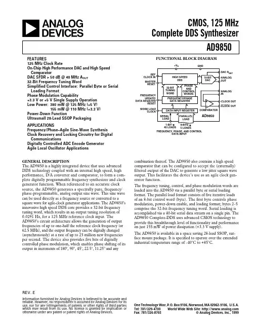
模拟器件 COMS 工艺,125MHZ 完整的DDS 频率合成器特点125M 时钟频率片内高性能DAC 转换器和高速比较器 DAC SFDR > 50 dB @ 40 MHz AOUT 32位频率控制字简单的控制接口:串行或并行装载模式可进行相位调节3.3V 或5V 单电源供电低功耗:380 mW @ 125 MHz (5 V)155 mW @ 110 MHz (3.3 V)省电模式超小型28引脚SSOP 封装 应用频率/相位——方便的正弦波合成 针对数字通信的时钟恢复和锁存电路 数控ADC 编码发生器 灵活的本机振荡器应用概述AD9850是一款高度集成的设备,采用先进的DDS 技术,结合内部高速,高性能的D / A 转换器和比较器,以构成一个完整的,数字可编程频率合成器和时钟发生器。
当连接到一个准确的时钟源时,AD9850产生一个频谱纯净,频率/相位可编程的模拟输出正弦波。
这个正弦波可以直接使用作为频率源,或者它可以被转变为方波作为精准时钟发生器使用。
AD9850先进的高速DDS 内核提供了一个32位的频率调谐字,这使得其在外部125MHZ 参考时钟的输入下,分辨率可达0.0291HZ 。
AD9850的电路架构使得其产生的最高输出频率为其参考的基准时钟频率的一半(或62.5兆MHZ ),而且其输出频率是数控可变的,速率高达72.310 次每秒。
该器件还提供了5位的相位控制字,从而使其输出信号的相位该变量可以为180°,90°,45°,22.5°,11.25°,以及它们的任意组合。
AD9850还包含一个高速比较器,该比较器可以输入经过滤波(外部)的片内DAC 产生的信号以生成一个低抖动方波输出。
这使得该芯片可以作为精准的时钟信号源。
AD9850的频率调谐,控制和相位调制字是通过一个并行字节或方式载入到芯片内部的。
并行载入格式由五个8位的控制字组成。
REV.EInformation furnished by Analog Devices is believed to be accurate and reliable. However, no responsibility is assumed by Analog Devices for its use, nor for any infringements of patents or other rights of third parties which may result from its use. No license is granted by implication or otherwise under any patent or patent rights of Analog Devices.aCMOS, 125 MHzComplete DDS SynthesizerAD9850FUNCTIONAL BLOCK DIAGRAMCLOCK OUTOUTSETREF CLOCK IN MASTER RESETFREQUENCY, PHASE, AND CONTROLDATA INPUTGENERAL DESCRIPTIONThe AD9850 is a highly integrated device that uses advanced DDS technology coupled with an internal high speed, high performance, D/A converter and comparator, to form a com-plete digitally programmable frequency synthesizer and clock generator function. When referenced to an accurate clock source, the AD9850 generates a spectrally pure, frequency/phase-programmable, analog output sine wave. This sine wave can be used directly as a frequency source or converted to a square wave for agile-clock generator applications. The AD9850’s innovative high speed DDS core provides a 32-bit frequency tuning word, which results in an output tuning resolution of 0.0291 Hz, for a 125 MHz reference clock input. TheAD9850’s circuit architecture allows the generation of output frequencies of up to one-half the reference clock frequency (or 62.5 MHz), and the output frequency can be digitally changed (asynchronously) at a rate of up to 23 million new frequencies per second. The device also provides five bits of digitallycontrolled phase modulation, which enables phase shifting of its output in increments of 180°, 90°, 45°, 22.5°, 11.25° and anycombination thereof. The AD9850 also contains a high speed comparator that can be configured to accept the (externally)filtered output of the DAC to generate a low jitter square wave output. This facilitates the device’s use as an agile clock gen-erator function.The frequency tuning, control, and phase modulation words are loaded into the AD9850 via a parallel byte or serial loading format. The parallel load format consists of five iterative loads of an 8-bit control word (byte). The first byte controls phase modulation, power-down enable, and loading format; bytes 2–5comprise the 32-bit frequency tuning word. Serial loading is accomplished via a 40-bit serial data stream on a single pin. The AD9850 Complete-DDS uses advanced CMOS technology to provide this breakthrough level of functionality and performance on just 155 mW of power dissipation (+3.3 V supply).The AD9850 is available in a space saving 28-lead SSOP, sur-face mount package. It is specified to operate over the extended industrial temperature range of –40°C to +85°C.FEATURES125 MHz Clock RateOn-Chip High Performance DAC and High Speed ComparatorDAC SFDR > 50 dB @ 40MHz A OUT 32-Bit Frequency Tuning WordSimplified Control Interface:Parallel Byte or Serial Loading FormatPhase Modulation Capability+3.3 V or +5 V Single Supply Operation Low Power:380 mW @ 125 MHz (+5 V)155 mW @ 110 MHz (+3.3 V)Power-Down FunctionUltrasmall 28-Lead SSOP PackagingAPPLICATIONSFrequency/Phase–Agile Sine-Wave Synthesis Clock Recovery and Locking Circuitry for Digital CommunicationsDigitally Controlled ADC Encode Generator Agile Local Oscillator ApplicationsOne Technology Way, P.O. Box 9106, Norwood, MA 02062-9106, U.S.A.Tel: 781/329-4700World Wide Web Site: Fax: 781/326-8703© Analog Devices, Inc., 1999AD9850BRS ParameterTemp Test LevelMin Typ MaxUnitsCLOCK INPUT CHARACTERISTICS Frequency Range +5 V Supply FullIV 1125MHz +3.3 V SupplyFull IV 1110MHz Pulsewidth High/Low +5 V Supply +25°C IV 3.2ns +3.3 V Supply +25°CIV4.1nsDAC OUTPUT CHARACTERISTICS Full-Scale Output Current R SET = 3.9 k Ω+25°C V 10.24mA R SET = 1.95 k Ω+25°C V 20.48mA Gain Error+25°C I –10+10% FS Gain Temperature Coefficient Full V 150ppm/°C Output Offset+25°C I 10µA Output Offset Temperature Coefficient Full V 50nA/°C Differential Nonlinearity +25°C I 0.50.75LSB Integral Nonlinearity+25°C I 0.51LSB Output Slew Rate (50Ω, 2 pF Load)+25°C V 400V/µs Output Impedance +25°C IV 50120k ΩOutput Capacitance +25°C IV 8pF Voltage Compliance+25°C I 1.5V Spurious-Free Dynamic Range (SFDR):Wideband (Nyquist Bandwidth)1 MHz Analog Out +25°C IV 6372dBc 20 MHz Analog Out +25°C IV 5058dBc 40 MHz Analog Out +25°C IV 4654dBc Narrowband40.13579 MHz ± 50 kHz +25°C IV 80dBc 40.13579 MHz ± 200 kHz+25°C IV 77dBc 4.513579 MHz ± 50 kHz/20.5 MHz CLK +25°C IV 84dBc 4.513579 MHz ± 200 kHz/20.5 MHz CLK +25°C IV 84dBc COMPARATOR INPUT CHARACTERISTICS Input Capacitance +25°C V 3pF Input Resistance +25°C IV 500k ΩInput Current+25°C I –12+12µA Input Voltage Range +25°C IV 0V DD V Comparator Offset*Full VI 3030mV COMPARATOR OUTPUT CHARACTERISTICS Logic “1” Voltage +5 V Supply Full VI +4.8V Logic “1” Voltage +3.3 V Supply Full VI +3.1V Logic “0” VoltageFull VI +0.4V Propagation Delay, +5 V Supply (15 pF Load)+25°C V 5.5ns Propagation Delay, +3.3 V Supply (15 pF Load)+25°C V 7ns Rise/Fall Time, +5 V Supply (15 pF Load)+25°C V 3ns Rise/Fall Time, +3.3 V Supply (15 pF Load)+25°C V 3.5ns Output Jitter (p-p)+25°C V 80ps CLOCK OUTPUT CHARACTERISTICS Clock Output Duty Cycle (Clk Gen. Config.)+25°CIV50 ± 10%REV. E–2–(V S= +5 V ؎ 5% except as noted, RSET = 3.9 k ⍀)AD9850–SPECIFICATIONSAD9850AD9850BRSParameter Temp Test Level Min Typ Max Units CMOS LOGIC INPUTS (Including CLKIN)Logic “1” Voltage, +5 V Supply+25°C I 3.5V Logic “1” Voltage, +3.3 V Supply+25°C I 3.0V Logic “0” Voltage+25°C I0.4V Logic “1” Current+25°C I12µA Logic “0” Current+25°C I12µA Input Capacitance+25°C V3pF POWER SUPPLY (A OUT = 1/3 CLKIN)+V S Current @:62.5 MHz Clock, +3.3 V Supply Full VI3048mA110 MHz Clock, +3.3 V Supply Full VI4760mA62.5 MHz Clock, +5 V Supply Full VI4464mA125 MHz Clock, +5 V Supply Full VI7696mAP DISS @:62.5 MHz Clock, +3.3 V Supply Full VI100160mW110 MHz Clock, +3.3 V Supply Full VI155200mW62.5 MHz Clock, +5 V Supply Full VI220320mW125 MHz Clock, +5 V Supply Full VI380480mWP DISS Power-Down Mode+5 V Supply Full V30mW +3.3 V Supply Full V10mW NOTES*Tested by measuring output duty cycle variation.Specifications subject to change without notice.TIMING CHARACTERISTICS*(V S = +5 V ؎ 5% except as noted, R SET = 3.9 k⍀)AD9850BRSParameter Temp Test Level Min Typ Max Unitst DS(Data Setup Time)Full IV 3.5nst DH(Data Hold Time)Full IV 3.5nst WH(W_CLK min. Pulsewidth High)Full IV 3.5nst WL(W_CLK min. Pulsewidth Low)Full IV 3.5nst WD(W_CLK Delay After FQ_UD)Full IV7.0nst CD(CLKIN Delay After FQ_UD)Full IV 3.5nst FH(FQ_UD High)Full IV7.0nst FL(FQ_UD Low)Full IV7.0nst CF(Output Latency from FQ_UD)Frequency Change Full IV18CLKIN Cycles Phase Change Full IV13CLKIN Cycles t FD(FQ_UD Min. Delay After W_CLK)Full IV7.0nst RH(CLKIN Delay After RESET Rising Edge)Full IV 3.5nst RL(RESET Falling Edge After CLKIN)Full IV 3.5nst RS(Minimum RESET Width)Full IV5CLKIN Cycles t OL(RESET Output Latency)Full IV13CLKIN Cycles t RR(Recovery from RESET)Full IV2CLKIN Cycles Wake-Up Time from Power-Down Mode+25°C V5µsNOTES*Control functions are asynchronous with CLKIN.Specifications subject to change without notice.REV. E–3–AD9850–4–REV. EABSOLUTE MAXIMUM RATINGS*Maximum Junction Temperature . . . . . . . . . . . . . . . +165°C V DD . . . . . . . . . . . . . . . . . . . . . . . . . . . . . . . . . . . . . . . . +6 V Digital Inputs . . . . . . . . . . . . . . . . . . . . . . . . . –0.7 V to +V S Digital Output Continuous Current . . . . . . . . . . . . . . . 5 mA DAC Output Current . . . . . . . . . . . . . . . . . . . . . . . . . 30 mA Storage Temperature . . . . . . . . . . . . . . . . . . –65°C to +150°C Operating Temperature . . . . . . . . . . . . . . . . .–40°C to +85°C Lead Temperature (Soldering 10 sec) . . . . . . . . . . . . +300°C SSOP θJA Thermal Impedance . . . . . . . . . . . . . . . . . . 82°C/W*Absolute maximum ratings are limiting values, to be applied individually, and beyond which the serviceability of the circuit may be impaired. Functional operability under any of these conditions is not necessarily implied. Exposure of absolute maximum rating conditions for extended periods of time may affect device reliability.EXPLANATION OF TEST LEVELSTest Level I –100% Production Tested.III –Sample Tested Only.IV –Parameter is guaranteed by design and characterizationtesting.V –Parameter is a typical value only.VI –All devices are 100% production tested at +25°C.100% production tested at temperature extremes for military temperature devices; guaranteed by design and characterization testing for industrial devices.CAUTIONESD (electrostatic discharge) sensitive device. Electrostatic charges as high as 4000V readily accumulate on the human body and test equipment and can discharge without detection.Although the AD9850 features proprietary ESD protection circuitry, permanent damage may occur on devices subjected to high energy electrostatic discharges. Therefore, proper E SD precautions are recommended to avoid performance degradation or loss of functionality.Application Note : Users are cautioned not to apply digital input signals prior to power-up of this device. Doing so may r esult in a latch-up condition.ORDERING GUIDEModel Temperature Range Package Description Package Option AD9850BRS–40°C to +85°CShrink Small Outline (SSOP)RS-28AD9850–5–REV. ETable I.Lead Function DescriptionsPin No.Mnemonic Function4–1,D0–D78-Bit Data Input. This is the 8-bit data port for iteratively loading the 32-bit frequency and 8-bit phase/28–25control word. D7 = MSB; D0 = LSB. D7 (Pin 25) also serves as the input pin for the 40-bit serial data word.5, 24DGND Digital Ground. These are the ground return leads for the digital circuitry.6, 23DVDD Supply Voltage Leads for digital circuitry.7W_CLK Word Load Clock. This clock is used to load the parallel or serial frequency/phase/control words.8FQ_UD Frequency Update. On the rising edge of this clock, the DDS will update to the frequency (or phase)loaded in the data input register, it then resets the pointer to Word 0.9CLKIN Reference Clock Input. This may be a continuous CMOS-level pulse train or sine input biased at 1/2V supply. The rising edge of this clock initiates operation.10, 19AGND Analog Ground. These leads are the ground return for the analog circuitry (DAC and comparator).11, 18AVDD Supply Voltage for the analog circuitry (DAC and comparator).12R SETThis is the DAC’s external R SET connection. This resistor value sets the DAC full-scale output current. For normal applications (F S I OUT = 10 mA ), the value for R SET is 3.9 k Ω connected to ground. The R SET /I OUT relationship is: I OUT = 32 (1.248 V/R SET ).13QOUTB Output Complement. This is the comparator’s complement output.14QOUT Output True. This is the comparator’s true output.15VINN Inverting Voltage Input. This is the comparator’s negative input.16VINPNoninverting Voltage Input. This is the comparator’s positive input.17DACBL (NC)DAC Baseline. This is the DAC baseline voltage reference; this lead is internally bypassed and shouldnormally be considered a “no connect” for optimum performance.20IOUTB The Complementary Analog Output of the DAC.21IOUT Analog Current Output of the DAC.22RESETReset. This is the master reset function; when set high it clears all registers (except the input register) and the DAC output will go to Cosine 0 after additional clock cycles—see Figure 19.PIN CONFIGURATIONSD3D7 MSB/SERIAL LOAD D6D5D4D2D1LSB D0RESETDVDDDGND DGND DVDD W CLK FQ UD CLKINAGND AGND IOUTB IOUTAVDD R SET QOUTB QOUT AVDD VINNVINP DACBL (NC)NC = NO CONNECTRBW # 100Hz START 0HzVBW 100HzATN # 30dB SWP 762 secSTOP 62.5MHz Figure 1.SFDR, CLKIN = 125 MHz/f OUT = 1 MHzRBW # 300Hz START 0HzVBW 300Hz ATN # 30dBSWP 182.6 sec STOP 62.5MHzFigure 2.SFDR, CLKIN = 125 MHz/f OUT= 41 MHzCh 1 500mV ⍀M 20.0ns Ch 1 1.58V D 500ps Runs AfterFigure 3.Typical Comparator Output Jitter, AD9850Configured as Clock Generator w/42 MHz LP Filter (40 MHz A OUT /125 MHz CLKIN)AD9850–Typical Performance Characteristics–6–REV. ERBW # 300Hz START 0HzVBW 300HzATN # 30dB SWP 182.6 secSTOP 62.5MHzFigure 4.SFDR, CLKIN = 125 MHz/f OUT = 20 MHzRBW # 3Hz CENTER 4.513579MHzVBW 3Hz ATN # 20dBSWP 399.5 sec SPAN 400kHzFigure 5.SFDR, CLKIN = 20.5 MHz/f OUT = 4.5 MHzOFFSET FROM 5MHz CARRIER – Hz–––––––––––100100k1kd B c10k Figure 6. Output Residual Phase Noise (5 MHz A OUT /125 MHz CLKIN)AD9850–7–REV. ECh1 1.00V ⍀ M 1.00ns Ch 1 1.74V Figure parator Output Rise Time (5 V Supply/15 pF Load)CLKIN – MHz140204060801001206852S F D R – d B66605856546462Figure 8.SFDR vs. CLKIN Frequency (A OUT = 1/3 of CLKIN)FREQUENCY OUT – MHz9080304010S U P P L Y C U R R E N T – m A203070605040Figure 9.Supply Current vs. A OUT Frequency (CLKIN = 125/110 MHz for 5 V/3.3 V Plot)Ch1 1.00V ⍀ M 1.00ns Ch 1 1.74VFigure parator Output Fall Time (5 V Supply/15 pF Load)CLOCK FREQUENCY – MHz0140204060801001209010S U P P L Y C U R R E N T –m A80504030207060Figure 11.Supply Current vs. CLKIN Frequency (A OUT = 1/3 of CLKIN)DAC I OUT – mA205S F D R – d B1015Figure 12.SFDR vs. DAC I OUT (A OUT = 1/3 of CLKIN)AD9850–8–REV. E5-POLE ELLIPTICALFigure 13.Basic AD9850 Clock Generator Application with Low-Pass FilterFigure 14.AD9850 Clock Generator Application in a Spread-Spectrum Receivera.Frequency/Phase –Agile Local Oscillatorb.Frequency/Phase –Agile Reference for PLLREFRFc.Digitally-Programmable ”Divide-by-N “ Function in PLLFigure 15.AD9850 Complete-DDS Synthesizer in Frequency Up-Conversion ApplicationsTHEORY OF OPERATION AND APPLICATIONThe AD9850 uses direct digital synthesis (DDS) technology, in the form of a numerically controlled oscillator, to generate a frequency/phase-agile sine wave. The digital sine wave is con-verted to analog form via an internal 10-bit high speed D/Aconverter, and an onboard high speed comparator is provided to translate the analog sine wave into a low jitter TTL/CMOS-compatible output square wave. DDS technology is an innova-tive circuit architecture that allows fast and precise manipulation of its output frequency under full digital control. DDS also enables very high resolution in the incremental selection of output frequency; the AD9850 allows an output frequency resolution of 0.0291 Hz with a 125 MHz reference clock ap-plied. The AD9850’s output waveform is phase-continuous when changed.The basic functional block diagram and signal flow of theAD9850 configured as a clock generator is shown in Figure 16.The DDS circuitry is basically a digital frequency divider function whose incremental resolution is determined by the frequency of the reference clock divided by the 2N number of bits in the tuning word. The phase accumulator is a variable-modulus counter that increments the number stored in it each time itreceives a clock pulse. When the counter overflows it wraps around, making the phase accumulator’s output contiguous.The frequency tuning word sets the modulus of the counter that effectively determines the size of the increment (∆ Phase) that gets added to the value in the phase accumulator on the next clock pulse. The larger the added increment, the faster the ac-cumulator overflows, which results in a higher output fre-quency. The AD9850 uses an innovative and proprietary algorithm that mathematically converts the 14-bit truncated value of the phase accumulator to the appropriate COS value.This unique algorithm uses a much reduced ROM look-up table and DSP techniques to perform this function, which contributes to the small size and low power dissipation of the AD9850. The relationship of the output frequency, reference clock, and tuning word of the AD9850 is determined by the formula:f OUT = (∆ Phase × CLKIN )/232where:∆ Phase =value of 32-bit tuning wordCLKIN =input reference clock frequency in MHz f OUT =frequency of the output signal in MHz The digital sine wave output of the DDS block drives the inter-nal high speed 10-bit D/A converter that reconstructs the sineAD9850–9–REV. EFigure 16.Basic DDS Block Diagram and Signal Flow of AD9850The reference clock frequency of the AD9850 has a minimum limitation of 1 MHz. The device has internal circuitry that senses when the minimum clock rate threshold has been exceeded and automatically places itself in the power-down mode. When in this state, if the clock frequency again exceeds the threshold,the device resumes normal operation. This shutdown mode prevents excessive current leakage in the dynamic registers of the device.The D/A converter output and comparator inputs are available as differential signals that can be flexibly configured in anymanner desired to achieve the objectives of the end-system. The typical application of the AD9850 is with single-ended output/input analog signals, a single low-pass filter, and generating the comparator reference midpoint from the differential DAC out-put as shown in Figure 13.Programming the AD9850The AD9850 contains a 40-bit register that is used to program the 32-bit frequency control word, the 5-bit phase modulation word and the power-down function. This register can be loaded in a parallel or serial mode.In the parallel load mode, the register is loaded via an 8-bit bus;the full 40-bit word requires five iterations of the 8-bit word.The W_CLK and FQ_UD signals are used to address and load the registers. The rising edge of FQ_UD loads the (up to) 40-bit control data word into the device and resets the address pointer to the first register. Subsequent W_CLK rising edges load the 8-bit data on words [7:0] and move the pointer to the next register. After five loads, W_CLK edges are ignored until either a reset or an FQ_UD rising edge resets the address pointer to the first register.In serial load mode, subsequent rising edges of W_CLK shift the 1-bit data on Lead 25 (D7) through the 40 bits of program-ming information. After 40 bits are shifted through, an FQ_UD pulse is required to update the output frequency (or phase).The function assignments of the data and control words are shown in Table III; the detailed timing sequence for updating the output frequency and/or phase, resetting the device, and powering-up/down, are shown in the timing diagrams of Figures 18–24.Note:There are specific control codes, used for factory test purposes, that render the AD9850 temporarily inoperable. The user must take deliberate precaution to avoid inputting the codes listed in Table II.wave in analog form. This DAC has been optimized for dynamic performance and low glitch energy as manifested in the low jitter performance of the AD9850. Since the output of the AD9850 is a sampled signal, its output spectrum follows the Nyquist sampling theorem. Specifically, its output spectrum contains the fundamental plus aliased signals (images) that occur at multiples of the Reference Clock Frequency ± the selected output frequency. A graphical representation of the sampled spectrum, with aliased images, is shown in Figure 17.REFERENCE CLOCKFREQUENCYFigure 17. Output Spectrum of a Sampled SignalIn this example, the reference clock is 100 MHz and the output frequency is set to 20 MHz. As can be seen, the aliased images are very prominent and of a relatively high energy level as deter-mined by the sin(x)/x roll-off of the quantized D/A converter output. In fact, depending on the fo/Ref Clk relationship, the first aliased image can be on the order of –3dB below the fun-damental. A low-pass filter is generally placed between the out-put of the D/A converter and the input of the comparator to further suppress the effects of aliased images. Obviously, con-sideration must be given to the relationship of the selected output frequency and the Reference Clock frequency to avoid unwanted (and unexpected) output anomalies.A good rule-of-thumb for applying the AD9850 as a clock generator is to limit the selected output frequency to <33% of Reference Clock frequency, thereby avoiding generating aliased signals that fall within, or close to, the output band of interest (generally dc-selected output frequency). This practice will ease the complexity (and cost) of the external filter requirement for the clock generator application.AD9850–10–REV. ETable II.Factory-Reserved Internal Test Control CodesLoading Format Factory-Reserved Codes Parallel 1) W0 = XXXXXX102) W0 = XXXXXX01Serial1) W32 = 1; W33 = 02) W32 = 0; W33 = 13) W32 = 1; W33 = 1Table III.8-Bit Parallel-Load Data/Control Word Functional AssignmentWord data[7]data[6]data[5]data[4]data[3]data[2]data[1]data[0]W0Phase-b4Phase-b3Phase-b2Phase-b1Phase-b0Power-Down Control Control (MSB) (LSB)W1Freq-b31Freq-b30Freq-b29Freq-b28Freq-b27Freq-b26Freq-b25Freq-b24(MSB)W2Freq-b23Freq-b22Freq-b21Freq-b20Freq-b19Freq-b18Freq-b17Freq-b16W3Freq-b15Freq-b14Freq-b13Freq-b12Freq-b11Freq-b10Freq-b9Freq-b8W4Freq-b7Freq-b6Freq-b5Freq-b4Freq-b3Freq-b2Freq-b1Freq-b0(LSB)OLD FREQ (PHASE)NEW FREQ (PHASE)*OUTPUT UPDATE CAN OCCUR AFTER ANY WORD LOAD AND IS ASYNCHRONOUS WITH THE REFERENCE CLOCKDATAW CLKREF CLKCOS OUTFQ UDFigure 18.Parallel-Load Frequency/Phase Update Timing SequenceAD9850COS OUTRESETt RH CLK DELAY AFTER RESET RISING EDGE3.5ns t RLRESET FALLING EDGE AFTER CLK 3.5nst RRRECOVERY FROM RESET 2 CLK CYCLES tRSMINIMUM RESET WIDTH 5 CLK CYCLES t OLRESET OUTPUT LATENCY 13 CLK CYCLESSYMBOL DEFINITION MIN SPECRESULTS OF RESET:– FREQUENCY/PHASE REGISTER SET TO 0– ADDRESS POINTER RESET TO W0– POWER-DOWN BIT RESET TO “0”– DATA INPUT REGISTER UNEFFECTEDFigure 19. Master Reset Timing SequenceDATA (W0)W CLKFQ UDREF CLKDAC STROBEFigure 20.Parallel-Load Power-Down Sequence/Internal OperationDATA (W0)W CLKFQ UDREF CLKFigure 21.Parallel-Load Power-Up Sequence/Internal OperationAD9850DATA (W0)(PARALLEL)W CLK FQ UDARE REQUIRED TO SHIFT IN REQUIRED W32–W34 DATA DATA (SERIAL)REQUIRED TO RESET CONTROL REGISTERSNOTE: FOR DEVICE START-UP IN SERIAL MODE, HARD-WIRE LEAD 2 AT “0”, LEAD 3 AT “1”, AND LEAD 4 AT “1”(SEE FIGURE 23).Figure 22.Serial-Load Enable SequenceFigure 23.Leads 2–4 Connection for Default Serial-Mode OperationDATA–W CLKFQ UDFigure 24.Serial-Load Frequency/Phase Update Sequence Table IV.40-Bit Serial-Load Word Function AssignmentW0Freq-b0 (LSB) W1Freq-b1W2Freq-b2W3Freq-b3W4Freq-b4W5Freq-b5W6Freq-b6W7Freq-b7W8Freq-b8W9Freq-b9W10Freq-b10W11Freq-b11W12Freq-b12W13Freq-b13W28Freq-b28W29Freq-b29W30Freq-b30W31Freq-b31 (MSB)W32ControlW33ControlW34Power-DownW35Phase-b0 (LSB)W36Phase-b1W37Phase-b2W38Phase-b3W39Phase-b4 (MSB) W14Freq-b14W15Freq-b15W16Freq-b16W17Freq-b17W18Freq-b18W19Freq-b19W20Freq-b20W21Freq-b21W22Freq-b22W23Freq-b23W24Freq-b24W25Freq-b25W26Freq-b26W27Freq-b27AD9850DATA (7) –W CLKFQUDFigure 25.Serial-Load Power-Down SequenceDIGITALINV DAC Output Comparator Output Comparator Input Digital InputsFigure 26.AD9850 I/O Equivalent CircuitsPCB LAYOUT INFORMATIONThe AD9850/CGPCB and AD9850/FSPCB evaluation boards (Figures 27–30) represent typical implementations of the AD9850 and exemplify the use of high frequency/high resolu-tion design and layout practices. The printed circuit board that contains the AD9850 should be a multilayer board that allows dedicated power and ground planes. The power and ground planes should be free of etched traces that cause discontinuities in the planes. It is recommended that the top layer of the multi-layer board also contain interspatial ground plane, which makes ground available for surface-mount devices. If separate analog and digital system ground planes exist, they should be con-nected together at the AD9850 for optimum results.Avoid running digital lines under the device as these will couple noise onto the die. The power supply lines to the AD9850should use as large a track as possible to provide a low-impedance path and reduce the effects of glitches on the power supply line.Fast switching signals like clocks should be shielded withground to avoid radiating noise to other sections of the board.Avoid crossover of digital and analog signal paths. Traces on opposite sides of the board should run at right angles to each other. This will reduce the effects of feedthrough through the circuit board. Use microstrip techniques where possible.Good decoupling is also an important consideration. The analog (AVDD) and digital (DVDD) supplies to the AD9850 are independent and separately pinned out to minimize coupling between analog and digital sections of the device. All analog and digital supplies should be decoupled to AGND and DGND,respectively, with high quality ceramic capacitors. To achieve best performance from the decoupling capacitors, they should be placed as close as possible to the device, ideally right upagainst the device. In systems where a common supply is used to drive both the AVDD and DVDD supplies of the AD9850, it is recommended that the system’s AVDD supply be used.Analog Devices, Inc., applications engineering support is avail-able to answer additional questions on grounding and PCB layout. Call 1-800-ANALOGD.Evaluation BoardsTwo versions of evaluation boards are available for the AD9850,which facilitate the implementation of the device for bench-top analysis, and serve as a reference for PCB layout. The AD9850/FSPCB is intended for applications where the device will primarily be used as frequency synthesizer. This version facilitates connection of the AD9850’s internal D/A converter output to a 50Ω spectrum analyzer input; the internal com-parator on the AD9850 DUT is not enabled (see Figure 28 for electrical schematic of AD9850/FSPCB). The AD9850/CGPCB is intended for applications using the device in the clock genera-tor mode. It connects the AD9850’s DAC output to the internal comparator input via a single-ended, 42 MHz low-pass, 5-pole Elliptical filter. This model facilitates the access of the AD9850’s comparator output for evaluation of the device as a frequency- and phase-agile clock source (see Figure 29 for electrical schematic of AD9850/CGPCB).Both versions of the AD9850 evaluation boards are designed to interface to the parallel printer port of a PC. The operating software runs under Microsoft ® Windows and provides a user-friendly and intuitive format for controlling the functionality and observing the performance of the device. The 3.5" floppy provided with the evaluation board contains an executable file that loads and displays the AD9850 function-selection screen.The evaluation board may be operated with +3.3 V or +5 V supplies. The evaluation boards are configured at the factory for an external reference clock input; if the onboard crystal clock source is used, remove R2.All trademarks are the property of their respective holders.。
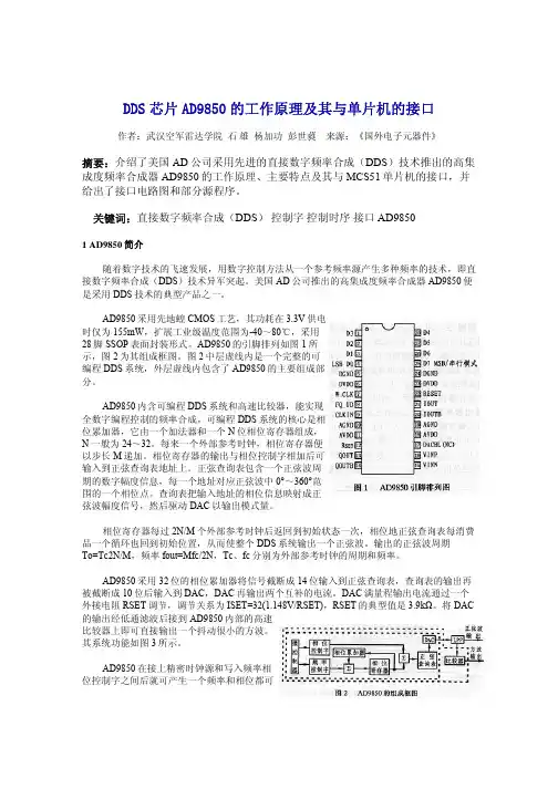
DDS芯片AD9850的工作原理及其与单片机的接口作者:武汉空军雷达学院石雄杨加功彭世蕤来源:《国外电子元器件》摘要:介绍了美国AD公司采用先进的直接数字频率合成(DDS)技术推出的高集成度频率合成器AD9850的工作原理、主要特点及其与MCS51单片机的接口,并给出了接口电路图和部分源程序。
关键词:直接数字频率合成(DDS)控制字控制时序接口 AD98501 AD9850简介随着数字技术的飞速发展,用数字控制方法从一个参考频率源产生多种频率的技术,即直接数字频率合成(DDS)技术异军突起。
美国AD公司推出的高集成度频率合成器AD9850便是采用DDS技术的典型产品之一。
AD9850采用先地蝗CMOS工艺,其功耗在3.3V供电时仅为155mW,扩展工业级温度范围为-40~80℃,采用28脚SSOP表面封装形式。
AD9850的引脚排列如图1所示,图2为其组成框图。
图2中层虚线内是一个完整的可编程DDS系统,外层虚线内包含了AD9850的主要组成部分。
AD9850内含可编程DDS系统和高速比较器,能实现全数字编程控制的频率合成。
可编程DDS系统的核心是相位累加器,它由一个加法器和一个N位相位寄存器组成,N一般为24~32。
每来一个外部参考时钟,相位寄存器便以步长M递加。
相位寄存器的输出与相位控制字相加后可输入到正弦查询表地址上。
正弦查询表包含一个正弦波周期的数字幅度信息,每一个地址对应正弦波中0°~360°范围的一个相位点。
查询表把输入地址的相位信息映射成正弦波幅度信号,然后驱动DAC以输出模式量。
相位寄存器每过2N/M个外部参考时钟后返回到初始状态一次,相位地正弦查询表每消费品一个循环也回到初始位置,从而使整个DDS系统输出一个正弦波。
输出的正弦波周期To=Tc2N/M,频率fout=Mfc/2N,Tc、fc分别为外部参考时钟的周期和频率。
AD9850采用32位的相位累加器将信号截断成14位输入到正弦查询表,查询表的输出再被截断成10位后输入到DAC,DAC再输出两个互补的电流。
应用笔记AN-587One Technology Way • P.O. Box 9106 • Norwood, MA 02062-9106 • 电话:781/329-4700 • 传真:781/326-8703 • 同步多个基于DDS 的频率合成器AD9850/AD9851作者:David Brandon ,ADI最佳布局简介许多应用要求产生两个或更多具有已知相位关系(如正交)的正弦波信号。
ADI 公司的AD9850和AD9851 DDS IC 能够提供这种信号。
本应用笔记详细说明了如何使两个或更多该器件同步,同时考虑了可能的相位误差源。
参考时钟(REF CLOCK)成功同步多个AD9850/AD9851的首要要求是所有DDS 的R EF CLK 输入之间的相位误差必须达到最小。
R EF CLK 边沿之间的任何相位差异都会导致DDS 输出处出现成比例的相位差异。
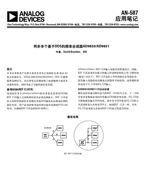
用户必须审慎考虑时钟分配在电路板PCB 上的布局,以确保REF CLK 边沿同步(见图1)。
AD9850/AD9851 R EF CLK 输入电路采用单端设计,因此,R EF CLK 必须具有最小的输入抖动和较短的上升/下降时间(建议5 ns 以下)。
R EF CLK 边沿上升时间较长会导致误差,因为输入电路的电压跳变点因器件不同而异。
这些属性同样适用于W_CLK 和FQ_UD 输入。
AD9850/AD9851 I/O 访问详情拥有边沿快速且路径适当的R EF CLK 信号之后,下一个时序要求是数据必须同步传输至DDS 程序寄存器。
FQ_UD 信号将数据传输至DDS 内核。
同步多个DDS 要求FQ_UD 的上升沿同时发生在所有DDS 上,如同EF CLK 一样。
另外,FQ_UD 必须发生在相对REF CLK 而言的适当时间。
图1. REF CLK 的分配AN-587图2. AD9850/AD9851功能框图图2为AD9850/AD9851的功能框图,两种器件之间仅存在较小差异。
多个基于DDS芯片AD9850/AD9851的合成器的同步方法一.概述在许多应用中,要求产生两个或者更多明确的相位相关的正弦信号,例如相位正交,美国ADI( Analog Devices Inc)公司推出的AD9850和AD9851 DDS集成芯片就可以提供这样的正弦信号。
本文详细地介绍了DDS芯片AD9850/AD9851的基本原理以及多个基于DDS芯片AD9850/AD9851的合成器的同步方法,提供了实现的步骤和指令,并且讨论了产生相位错误的可能原因。
二.基本原理1、AD9850/AD9851的基本特点和工作原理AD9850/AD9851是AD公司生产的最高时钟为125MHz、采用先进的CMOS技术的直接频率合成器。
它结合一个片内高速、高性能DAC和比较器构成一个完整的数字控制可编程频率合成器,是具有时钟产生功能的高集成度芯片。
由于采用了CMOS技术,其功耗较小,在+5V 电源供电,125MHz时钟时,能以380mW的功率工作。
AD9850/AD9851具有以下特点:a)125MHz的时钟频率;b)集成在一块集成电路芯片上的高性能DAC以及高速比较器;c)5bits相位调制;d)32bits频率控制字;e)40MHz模拟输出时,DAC输出的抑制寄生动态范围SFDR>50dB;f) +5V电源供电,125MHz时钟时,功率为380mW;g)简化的控制接口,并行或串行输入形式;h)极小的28管脚表面封装形式。
图1为AD9850/AD9851的功能模块图。
由此可以看出,这两种芯片只有微小的区别,那就是AD9851有一个6x时钟乘法器和MUX,而AD9850没有。
在DDS (Direct Digital Synthesis,直接数字式频率合成)内核前有两个寄存器,第一个是移位寄存器,它接收5字节的并行数据或者40位的串行数据,由字输入时钟信号W_CLK将数据锁存到该寄存器中。
当第二个寄存器由FQ_UD信号触发后,它就会将移位寄存器中的内容送到DDS内核,此过程在系统时钟信号的下一个上升沿完成。
DDS1.模块功能:DDS模块主要采用AD9850、AD812、125MHz有源晶振等器件,DDS是新一代的信号产生方式,它把一系列数字量形式的信号通过DAC转换成模拟量形式的信息。
它的工作方式是利用高速存储器作查询表,然后通过高速DAC产生已经用数字形式存入的波形。
与其他频率合成方法相比,DDS具有频率转换时间短、频率分辨率高、输出相位连续、可编程、全数字化仪与集成等突出优点。
本模块原理图见图1。
图 12.主要器件:(1) AD9850:(a)器件功能:AD9850是AD公司生产的采用先进的CMOS技术的直接频率合成器,主要由可编程DDS系统、高性能模数变换器(DAC)和高速比较器三部分构成,能实现全数字编程控制的频率合成,并且有时钟产生功能,能产生最高125MHZ 的时钟频率,功耗低。
它采用32位的相位累加器将信号截断成14位输入到正弦查询表,查询表的输出再被截断成10位后输入到DAC,DAC再输出两个互补的电流。
DAC满量程输出电流通过一个外接电阻REST调节,调节关系为Iset=32/(1.248V/RSET)。
(b) 器件引脚:AD9850引脚图如图2所示。
D0—D7:8比特数据输入端。
这是一个用于重复输入32比特频率和8比特相位/控制字的8比特数据输入端,D7是最高位,它还是40比特串行数据输入端口。
DGND:数字电路地。
DVDD:数字电路电源。
W_CLK:控制字输入时钟。
此时钟用来控制并行或串行输入频率/相位控制字。
FQ_UD:频率更新时钟。
在此时钟的上升沿,DDS将刷新已输入到数据输入寄存器中的频率(或相位)字,是输入数据寄存器归。
CLKIN:参考时钟输入。
AGND:模拟电路地。
AVDD:模拟电路电源。
Rset:DAC外部电阻Rset连接处。
QOUTB:输出为补充,是比较器的补充输出。
图2QOUT:输出为真。
是比较器的真正输出。
RESET:重新设置。
IOUT:DAC的模拟电源输出。
1、在您收到鑫悦电子AD9850模块后,请先大致熟悉AD9850模块:
SINA、SINB是正弦波形输出
QN、QP是方波输出
发光二极管是VCC电源指示灯(如果通电后,LED1不亮,请立即断电检查) 该模块可以用作并行和串行两种模式。
如何使用串行模式,请参考文件夹“串行”
2、按照下图连接好硬件。
然后把并行鑫悦电子ad9850模块测试程序
“ad9850.hex”烧到单片机AT89S52。
如果一切都顺利,那么您用示波器马上就能测出波形了。
3、如果没有波形输出,请按照以下办法解决。
是不是掌柜把AD9851的资料发给你了?那样肯定没有波形。
测试程序是按照A T89S52来写的,您是不是用别的单片机了。
程序运行了吗?如果单片机没有跑起来,那肯定没波形。
陕西理工学院毕业设计[摘要]本设计使用51单片机对DDS芯片进行控制,利用DDS造波的方法产生需要的正弦信号.用户可以根据需要对芯片设定一个频率值或相位值,通过单片机传输芯片控制字对芯片输出的频率和相位进行调节,达到用户所要求的信号。
本设计采用模块化设计的方法,不同的模块为实现不同的功能而设计,总体由单片机控制协调工作。
利用51单片机控制DDS芯片造波,具有如下优越性:1.造价低廉。
51系列单片机应用广泛,价格低廉,比较容易购买,DDS芯片价格较单片机稍高,但与价格成百上千的成品信号发生器相比,本设计经济优势显著。
2.电路简单。
本设计利用单片机进行数字化控制,外围元件较少,仅需辅以少量的阻容元件用于电流电压匹配控制以及滤波电路既可。
3.频率控制准确高效。
数字化控制的最大优点即控制准确。
本设计选用的DDS芯片内置32位高速数模转换器,分辨率高,响应快。
[关键词]51单片机;DDS造波;频率;The Design of Sinusoidal Signal Generator Based on SinglechipFan Pengxing[Abstract]: The design use 51series’ singlechip to control DDS chip’s ing DDS method to produce sine signal.The user can set a frequency or phase value freely.To achieve the user request signal,the singlechip need sending a control word to DDS chip,which determines the frequency and phase values.This design uses the modular design method, different modules designed for different functions.Singlechip responsible for coordination of all work.The benefits of DDS method to produce sine signal as follows:1.low cost. The 51 series’singlechip’s application are range,so they have low price and are easy to purchase.The price of DDS chip is slightly higher than singlechip.but to compare with the commodity signal generator which values hundreds even thousands,the advantages of this design is obvious.2.Simple circuit..Benefits which digital control takes is Peripheral element is less.It’s only need a few capacitance and resistance element for crrent and voltage matching and filter.3.Frequency control is accurate and efficient.Frequency control is accurate and efficient.This design using DDS chip with 32 bit high speed D/A converter,which has a high resolution, fast response.[Key words]: 51 singlechip;DDS method to produce signal;Frequency;第 1 页共 64 页目录The Design of Sinusoidal Signal Generator Based on Singlechip (1)引言 (4)1 绪论 (5)1.1单片机在函数信号发生器中的应用 (5)1.2发展现状 (5)1.3项目可行性研究 (5)1.4设计任务和要求 (6)2.方案及工作原理 (6)2.1方案设计 (6)2.1.1方案一 (6)2.1.2 方案二 (6)2.1.3 方案三 (6)2.1.4 方案四 (6)2.2DDS工作原理 (7)2.3DDS移相原理 (7)3.电路设计 (8)3.1设计思路 (8)3.2元件选型 (8)3.3系统总体框图 (8)3.4STC89C52RC单片机 (9)3.5AD9850芯片 (10)3.5.1 AD9850芯片简介 (10)3.5.2 AD9850工作方式介绍 (11)3.5.3相位控制字的计算 (11)3.61602LCD显示屏 (12)3.6.1液晶概述 (12)3.6.2接口信号说明 (12)3.6.3 1602地址说明 (13)3.6.4 1602指令码说明 (13)3.6.5 1602LCD写操作时序图 (13)3.7低通滤波器的设计 (14)3.7.1低通滤波器 (14)3.7.2低通滤波器的选型 (14)3.7.3低通滤波器的设计 (14)3.8总电路原理图 (16)3.9硬件调试 (16)3.10参数测量及误差分析 (20)3.10.1参数测量 (20)3.10.2误差分析 (20)4.软件设计 (21)4.1主程序流程图 (21)4.2源程序 (22)总结 (23)致谢 (24)参考文献 (25)附录 (26)附录A:文献原文 (26)附录B:外文文献翻译; (34)附录C:电路原理图 (41)附录D:元器件清单表。
精心整理第13章DDS 芯片AD9850/AD9851的设计13.1硬件设计信号源作为现代电子产品设计和生产中的重要工具,必须满足高精度、高速度、高分辨率等要求。
本章基于DDS(DirectDigitalSynthesis,直接数字频率合成)技术,采用AD9850DDS 芯片,采用F169单片机作为控制芯片,实现一种了简易信号发生器的设计,该信号发生器具有输出频率范围宽,可以输出正弦和方波两种波形,与键盘结合易于实现全数字化的设计。
(DDS )80℃,采用28图13-3系统的10位后输入到DAC ,DAC 再输出两个互补的电流。
DAC 满量程输出电流通过一个外接电阻set R 调节,调节关系为set I =32(1.148V/RSET),set R 的典型值是3.9K Ω。
将DAC 的输出经低通滤波后接到AD9850内部的高速比较器上即可直接输出一个抖动很小的方波。
其系统功能如图3-3所示。
AD9850在接上精密时钟源和写入频率相位控制字之后就可产生一个频率和相位都可编程控制的模拟正弦波输出,此正弦波可直接用作频率信号源或经内部的高速比较器转换为方波输出[23]。
在125MHz 的时钟下,32位的频率控制字可使AD9850的输出频率分辨率达0.0291Hz ;并具有5位相位控制位,而且允许相位按增量180,45,90,22.5,11.25或这些值的组合进行调整。
精心整理图13-3AD9850的内部结构13.1.2AD9850的控制字与控制时序AD9850有40位控制字,32位用于频率控制,5位用于相位控制。
1位用于电源休眠(Powerdown )控制,2位用于选择工作方式。
这40位控制字可通过并行方式或串行方式输入到AD9850,在并行装入方式中,通过8位总线D0…D7将可数据输入到寄存器,在重复5次之后再在FQ_UD 上升沿把40位数据从输入寄存器装入到频率/相位数据寄存器(更新DDS 输出频率和相位),同时把地址指针复位到第一个输入寄存器。
海纳电子资讯网:www.fpga-arm.com目录摘要 —————————————————————————2 创新之处 ———————————————————————2 关键词 ————————————————————————2 引言 —————————————————————————2 系统工作原理 —————————————————————3 直接数字频率合成 ———————————————————4 DDS 基本原理及性能特点 —————————————————5 采用 DDS 的 AD9851 ———————————————————6 AD9851 的原理 —————————————————————7 AD9851 在信号源中的应用 ————————————————8 AD9851 在本系统的应用电路 ———————————————9 低通滤波器(LPF) ——————————————————10 锁相环频率合成 ———————————————————11 锁相环频率合成 MC145151 在本电路中的应用 ————————12 压控振荡器(VCO) ———————————————————12 缓冲放大器 ——————————————————————13 单片机控制的整体电路 —————————————————14 功率放大 ———————————————————————15 本系统的软件设计 ———————————————————15 总调试 ————————————————————————25 结束语 ————————————————————————25 DDS 短波信号发生器技术指标 ——————————————26 所采用的仪器设备 ———————————————————26 所用软件 ———————————————————————26 参考文献 ———————————————————————26 参考网站 ———————————————————————27www.fpga-ar m1.海纳电子资讯网:www.fpga-arm.comDDS 短波信号发生器摘要: 本文主要介绍的是采用直接数字频率合成的短波信号发生器, 它 主要以微电脑控制部分、直接数字频率合成(DDS)部分、数字锁相 环频率合成部分、背光液晶显示部分、功率放大部分等组成。
一、原理图
二、模块说明
1、
注意实物与原理图的对应关系,电路板上也做了功能标识。
2、
使用非常简单,仅仅使用主接口,即能完成全部工作。
3、
主接口红色部分(即P1-1,P1-2)为外接电源。
1引脚为+5V, 2引脚为地,接反会烧毁芯片。
注意外接电源需要纯净,否则,影响正弦信号高频特性。
4、
主接口粉色部分(即P1-3,P1-4,P1-5)为单片机控制I/O。
5、 主接口青色部分(即P1-6,P1-7,P1-8)为模块输出引脚。
6脚为方波输出,7脚为正弦波滤波后输出,8脚为正弦波未滤波输出。
6、 辅助接口天蓝色部分对应原理图P4和主接口P1-7功能相同,可以用于示波器观测。