UC2824中文资料
- 格式:pdf
- 大小:387.33 KB
- 文档页数:8
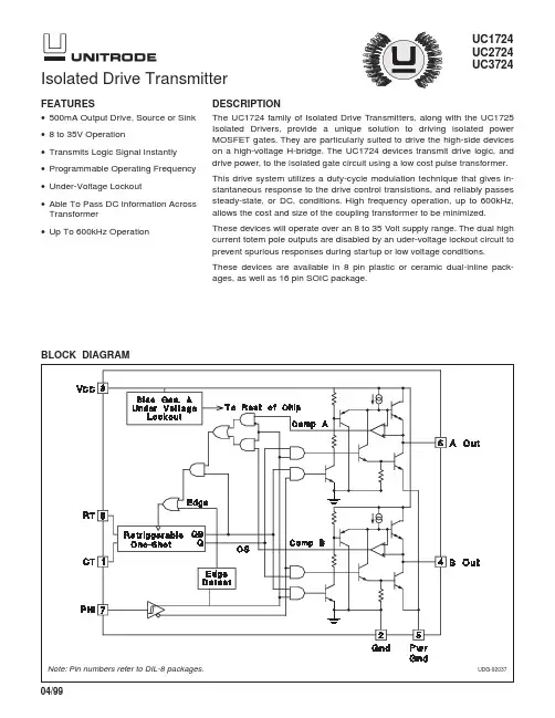
BLOCK DIAGRAM•Complementary Outputs•Practical Operation Switching Frequencies to 1MHz•50ns Propagation Delay to Output •High Current Dual Totem Pole Outputs (1.5A Peak)•Wide Bandwidth Error Amplifier •Fully Latched Logic with Double Pulse Suppression•Pulse-by-Pulse Current Limiting •Soft Start / Max. Duty Cycle Control •Under-Voltage Lockout with Hysteresis •Low Start Up Current (1.1 mA)•Trimmed Bandgap Reference (5.1V ± 1%)The UC1824 family of PWM control ICs is optimized for high fre-quency switched mode power supply applications. Particular care was given to minimizing propagation delays through the comparators and logic circuitry while maximizing bandwidth and slew rate of the error amplifier. This controller is designed for use in either current-mode or voltage mode systems with the capability for input voltage feed-forward.Protection circuitry includes a current limit comparator with a 1V threshold, a TTL compatible shutdown port, and a soft start pin which will double as a maximum duty cycle clamp. The logic is fully latched to provide jitter free operation and prohibit multiple pulses at an out-put. An under-voltage lockout section with 800mV of hysteresis as-sures low start up current. During under-voltage lockout, the outputs are high impedance.These devices feature totem pole outputs designed to source and sink high peak currents from capacitive loads, such as the gate of a power MOSFET . The on state is designed as a high level.UC1824UC2824UC3824High Speed PWM ControllerFEATURESDESCRIPTIONUDG-92034-1CONNECTION DIAGRAMSDIL-16 (Top View)J Or N PackageSOIC-16 (Top View)DW PackageUC3824ELECTRICAL CHARACTERISTICS:Unless otherwise stated,these specifications apply for , R T = 3.65k, C T = 1nF, V CC= 15V, -55°C<T A <125°C for the UC1824, –40°C<T A <85°C for the UC2824, and 0°C<T A <70°C for the UC3824, T A =T J.UC1824UC3824PARAMETERSTEST CONDITIONSUC2824MIN TYP MAX MIN TYP MAX UNITS Reference Section Output Voltage T J = 25°C, I O = 1mA 5.055.105.15 5.005.10 5.20V Line Regulation 10V < V CC < 30V 220220mV Load Regulation1mA < I O < 10mA 520520mV Temperature Stability*T MIN < T A < T MAX0.20.40.20.4mV/°C Total Output Variation*Line, Load, Temperature 5.00 5.20 4.955.25V Output Noise Voltage*10Hz < f < 10kHz 5050µV Long Term Stability*T J = 125°C, 1000hrs.525525mV Short Circuit Current V REF = 0V -15-50-100-15-50-100 mA Oscillator Section Initial Accuracy*T J = 25°C360400440360400440kHz Voltage Stability*10V < V CC < 30V 0.220.22%Temperature Stability*T MIN < T A < T MAX 55%Total Variation*Line, Temperature340460340460kHzPACKAGE PIN FUNCTIONFUNCTION PINN/C 1 INV 2NI3E/A Out 4Clock 5N/C 6R T 7C T 8Ramp 9Soft Start 10N/C 11ILIM/SD 12Gnd 13Out14Pwr Gnd 15N/C 16V C17INV OUT 18V CC19V REF 5.1V20PLCC-20 & LCC-20(Top View)Q & L PackagesABSOLUTE MAXIMUM RATINGS (Note 1)Supply Voltage (Pins 13, 15). . . . . . . . . . . . . . . . . . . . . . . . 30V Output Current, Source or Sink (Pins 11, 14)DC. . . . . . . . . . . . . . . . . . . . . . . . . . . . . . . . . . . . . . . . . . . . 0.5A Pulse (0.5µs). . . . . . . . . . . . . . . . . . . . . . . . . . . . . . . . . . . 2.0A Analog Inputs(Pins 1, 2, 7). . . . . . . . . . . . . . . . . . . . . . . . . . . . . . . -0.3V to 7V (Pin 8, 9). . . . . . . . . . . . . . . . . . . . . . . . . . . . . . . . . . -0.3V to 6V Clock Output Current (Pin 4). . . . . . . . . . . . . . . . . . . . . . . -5mA Error Amplifier Output Current (Pin 3). . . . . . . . . . . . . . . . 5mA Soft Start Sink Current (Pin 8) . . . . . . . . . . . . . . . . . . . . . 20mA Oscillator Charging Current (Pin 5). . . . . . . . . . . . . . . . . . -5mA Power Dissipation . . . . . . . . . . . . . . . . . . . . . . . . . . . . . . . . 1W Storage Temperature Range . . . . . . . . . . . . . . -65°C to +150°C Lead Temperature (Soldering, 10 seconds). . . . . . . . . . 300°C Note 1: All voltages are with respect to GND (Pin 10); all cur-rents are positive into, negative out of part; pin numbers refer to DIL-16 package.Note 3: Consult Unitrode Integrated Circuit Databook for ther-mal limitations and considerations of package.UC1824UC3824PARAMETERSTEST CONDITIONSUC2824MIN TYP MAX MIN TYP MAXUNITS Oscillator Section (cont.)Clock Out High 3.9 4.5 3.94.5V Clock Out Low 2.3 2.9 2.3 2.9V Ramp Peak * 2.6 2.8 3.0 2.6 2.8 3.0V Ramp Valley *0.7 1.0 1.250.7 1.0 1.25V Ramp Valley to Peak * 1.61.82.0 1.61.82.0V Error Amplifier Section Input Offset Voltage 1015mV Input Bias Current 0.630.63µA Input Offset Current 0.110.11µA Open Loop Gain 1V < V O < 4V 60956095dB CMRR 1.5V < V CM < 5.5V 75957595dB PSRR 10V < V CC < 30V 8511085110dB Output Sink Current V PIN 3 = 1V 1 2.51 2.5mA Output Source Current V PIN 3 = 4V -0.5-1.3-0.5-1.3mA Output High Voltage I PIN 3 = -0.5mA 4.0 4.7 5.0 4.0 4.7 5.0 V Output Low Voltage I PIN 3 = 1mA 00 .5 1.000.5 1.0V Unity Gain Bandwidth *3 5.53 5.5MHz Slew Rate *612612V/µs PWM Comparator Section Pin 7 Bias Current V PIN 7 = 0V -1-5-1-5µA Duty Cycle Range080085%Pin 3 Zero DC Threshold V PIN 7 = 0V 1.11.25 1.11.25V Delay to Output *50805080ns Soft-Start Section Charge Current V PIN 8 = 0.5V 39203920µA Discharge Current V PIN 8 = 1V 11mA Current Limit / Shutdown Section Pin 9 Bias Current 0 < V PIN 9 < 4V 1510µA Current Limit Threshold 0.9 1.0 1.10.9 1.0 1.1V Shutdown Threshold 1.251.40 1.55 1.251.40 1.55V Delay to Output 50805080ns Output Section Output Low Level I OUT = 20mA0.250.400.250.40V I OUT = 200mA1.22.21.22.2V Output High Level I OUT = -20mA13.013.513.013.5V I OUT = -200mA12.013.012.013.0V Collector Leakage V C = 30V 10050010500µA Rise/Fall Time *CL = 1nF 30603060ns Under-Voltage Lockout Section Start Threshold 8.89.29.68.89.29.6V UVLO Hysteresis0.40.8 1.20.40.8 1.2V Supply Current Section Start Up Current V CC = 8V 1.1 2.5 1.1 2.5mA ICC V PIN 1, V PIN 7, V PIN 9 = 0V; V PIN 2 = 1V22332233mAUnless otherwise stated,these specifications apply for , R T = 3.65k, C T= 1nF, V CC = 15V, -55°C<T A <125°C for the UC1824, –40°C<T A <85°C for the UC2824, and 0°C<T A <70°C for the UC3824, T A =T J.* This parameter not 100% tested in production but guaranteed by design.UC3824ELECTRICAL CHARACTERISTICS (cont.)High speed circuits demand careful attention to layout and component placement. T o assure proper performance of the UC1824 follow these rules: 1) Use a ground plane.2) Damp or clamp parasitic inductive kick energy from the gate of driven MOSFET s. Do not allow the output pins to ring below ground. A series gate resistor or a shunt 1 Amp Schottky diode at the output pin will serve this purpose. 3)Bypass V CC , V C , and V REF . Use 0.1µF monolithic ceramic capacitors with low equivalent series inductance. Allow less than 1 cm of total lead length for each capacitor be-tween the bypassed pin and the ground plane. 4) Treat the timing capacitor, C T , like a bypass capacitor.UC2824UC3824Open Loop Frequency Response Unity Gain Slew RateSimplified SchematicError Amplifier CircuitSynchronized OperationUC1824 Printed Circuit Board Layout ConsiderationsTwo Units in Close ProximityGeneralized SynchronizationOscillator CircuitUC3824µPrimary Output Deadtime vs C T (3k ≤ R T ≤ 100k)Timing Resistance vs Frequency8010012014016010k100k470pF1.0nF1MFREQ (Hz)T (n s )D Primary Output Deadtime vs FrequencyT C ()°T (ns)NO 01020304050607080-75-50-250255075100125Typical Non-Overlap Time (T NO ) Over TemperatureNon-Overlap Time (T NO )UC3824 Forward Technique for Off-Line Voltage Mode ApplicationConstant Volt-Second Clamp CircuitThe circuit shown here will achieve a constant volt-sec-ond product clamp over varying input voltages. Theramp generator components, R T and C R are chosen sothat the ramp at Pin 9 crosses the 1V threshold at thesame time the desired maximum volt-second productis reached. The delay through the functional nor blockmust be such that the ramp capacitor can be com-pletely discharged during the minimum deadtime.Output SectionSimplified Schematic Rise/Fall Time (C L=1nF)Rise/Fall Time (C L=10nF)Saturation CurvesUC3824 Open Loop Laboratory Test FixtureUDG-92036-2This test fixture is useful for exercising many of the UC1824’s functions and measuring their specifications.As with any wideband circuit, careful grounding and by-pass procedures should be followed. The use of a ground plane is highly recommended.UNITRODE CORPORATION7 CONTINENTAL BLVD. • MERRIMACK, NH 03054 TEL. (603) 424-2410 • FAX (603) 424-3460IMPORTANT NOTICETexas Instruments and its subsidiaries (TI) reserve the right to make changes to their products or to discontinue any product or service without notice, and advise customers to obtain the latest version of relevant information to verify, before placing orders, that information being relied on is current and complete. All products are sold subject to the terms and conditions of sale supplied at the time of order acknowledgement, including those pertaining to warranty, patent infringement, and limitation of liability.TI warrants performance of its semiconductor products to the specifications applicable at the time of sale in accordance with TI’s standard warranty. Testing and other quality control techniques are utilized to the extent TI deems necessary to support this warranty. Specific testing of all parameters of each device is not necessarily performed, except those mandated by government requirements.CERTAIN APPLICATIONS USING SEMICONDUCTOR PRODUCTS MAY INVOLVE POTENTIAL RISKS OF DEATH, PERSONAL INJURY, OR SEVERE PROPERTY OR ENVIRONMENTAL DAMAGE (“CRITICAL APPLICATIONS”). TI SEMICONDUCTOR PRODUCTS ARE NOT DESIGNED, AUTHORIZED, OR WARRANTED TO BE SUITABLE FOR USE IN LIFE-SUPPORT DEVICES OR SYSTEMS OR OTHER CRITICAL APPLICATIONS. INCLUSION OF TI PRODUCTS IN SUCH APPLICATIONS IS UNDERSTOOD TO BE FULLY AT THE CUSTOMER’S RISK.In order to minimize risks associated with the customer’s applications, adequate design and operating safeguards must be provided by the customer to minimize inherent or procedural hazards.TI assumes no liability for applications assistance or customer product design. TI does not warrant or represent that any license, either express or implied, is granted under any patent right, copyright, mask work right, or other intellectual property right of TI covering or relating to any combination, machine, or process in which such semiconductor products or services might be or are used. TI’s publication of information regarding any third party’s products or services does not constitute TI’s approval, warranty or endorsement thereof.Copyright © 1999, Texas Instruments Incorporated。