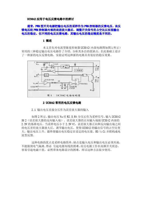
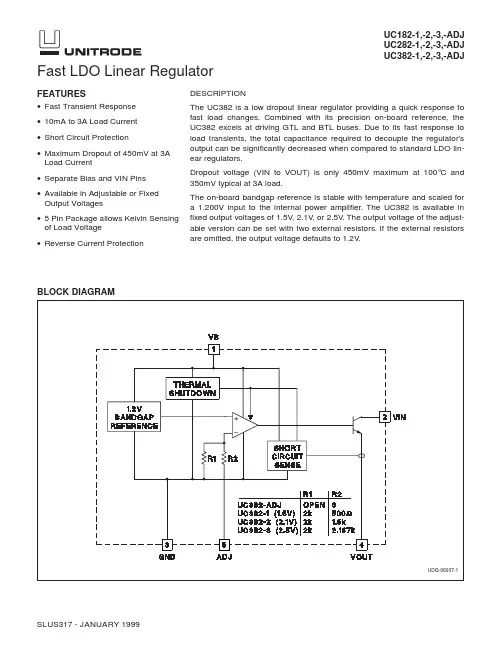
UC2872资料
- 格式:pdf
- 大小:180.52 KB
- 文档页数:7
UC1872
UC2872
UC3872
07/99FEATURES
•Controls Different Types of Lamps:Cold Cathode Fluorescent, Neon, andGas Discharge
•Zero Voltage Switching (ZVS) ofPush-Pull Drivers
•Accurate Control of Lamp Current
•Variable Lamp Intensity Control
•1µA Disable Current
•4.5V to 24V Operation
•Open Lamp Detection CircuitryDESCRIPTION
TheUC3872isaresonantlampballastcontrolleroptimizedfordriving
coldcathodefluorescent,neon,andothergasdischargelamps.Theres-
onantpowerstagedevelopsasinusoidallampdrivevoltage,andmini-
mizesswitchinglossandEMIgeneration.Lampintensityadjustmentis
accomplishedwithabuckregulator,whichissynchronizedtotheexternal
powerstage’sresonantfrequency.Suitableforautomotiveandbattery
powered applications, the UC3872 draws only 1µA when disabled.
Softstartandopenlampdetectcircuitryhavebeenincorporatedtomini-
mizecomponentstresses.Openlampdetectionisenabledatthecomple-
tionofasoftstartcycle.Thechipisoptimizedforsmoothdutycycle
control to 100%.
Otherfeaturesincludeaprecision1.2%reference,undervoltagelockout,
and accurate minimum and maximum frequency control.
Resonant Lamp Ballast Controller
4
6
53
2
12
131
147
8+–
0.5VSYNCOUTSENSEOSCILLATOR
GND+––
+OPENLAMPDETECT+–
+–UVLO3.0VREF10
9
11
R
STTOGGLE50k
50k
50kPUSHPULLOUTPUTSN-CHANNELVC
AOUT
BOUT
COUT
PGND0.1V
PWM1
0.2V200µA
ZERODETECT
ZDCTSSINVCOMPENBLREFVCC
1.5V20µA(HIGH=ENABLE)
BUCKDRIVEP-CHANNELEABLOCK DIAGRAM
UDG-99112Note:Pin numbers shown are for DIP package.application
INFO
available元器件交易网www.cecb2b.comUC1872
UC2872
UC3872
ELECTRICAL CHARACTERISTICS:Unless otherwise stated, these parameters apply for TJ=−55°C to +125°C for theUC1872, –40°C to +85°C for the UC2872,−0°C to +70°C for the UC3872; VCC= 5V, VC = 15V, VENBL= 5V, CT = 1nF, ZD = 1V.
PARAMETERTEST CONDITIONSMINTYPMAXUNITS
Reference Section
Output VoltageTJ= 25°C2.9633.0003.037V
Over Temperature2.9403.0003.060V
Line RegulationVCC = 4.75V to 18V10mV
Load RegulationIO= 0 to−5mA10mV
Oscillator Section
Free Running FrequencyTJ= 25°C576878kHz
Maximum Synchronization FrequencyTJ= 25°C160200240kHz
Charge CurrentVCT= 1.5V180200220µA
Voltage Stability2%
Temperature Stability48%
Zero Detect Threshold0.460.50.56V
Error Amp Section
Input VoltageVO= 2V1.4451.4751.505V
Input Bias Current−0.4−2µA
Open Loop GainVO= 0.5 to 3V6590dB
Output HighVINV= 1.3V3.13.53.9VABSOLUTE MAXIMUM RATINGS
Analog Inputs. . . . . . . . . . . . . . . . . . . . . . . . . . . . .−0.3 to +10VVCC, VC Voltage. . . . . . . . . . . . . . . . . . . . . . . . . . . . . . . .+24VZD Input CurrentHigh Impedance Source. . . . . . . . . . . . . . . . . . . . . .+10mAZD Input VoltageLow Impedance Source. . . . . . . . . . . . . . . . . . . . . . . .+24VPower Dissipation at TA= 25°C. . . . . . . . . . . . . . . . . . . . . .1WStorage Temperature. . . . . . . . . . . . . . . . . . .−65°C to +150°CLead Temperature. . . . . . . . . . . . . . . . . . . . . . . . . . . . . .300°C
Note1:Currentsarepositiveinto,negativeoutofthespecifiedterminal.
Note2:ConsultPackagingSectionofDatabookforthermallimi-tations and considerations of package.
DIL-14 (TOP VIEW)
N PackagePLCC-20 (Top View)
Q PackageCONNECTION DIAGRAMS
SOIC-16,SSOP-16 (TOP VIEW)DW,M Package元器件交易网www.cecb2b.comUC1872
UC2872
UC3872
ELECTRICAL CHARACTERISTICS:Unless otherwise stated, these parameters apply for TJ=−55°C to +125°C for theUC1872, –40°C to +85°C for the UC2872,−0°C to +70°C for the UC3872; VCC= 5V, VC = 15V, VENBL= 5V, CT = 1nF, ZD = 1V.
PARAMETERTEST CONDITIONSMINTYPMAXUNITS
Error Amp Section (cont.)
Output LowVINV= 1.7V0.10.2V
Output Source CurrentVINV= 1.3V, VO= 2V–350–500µA
Output Sink CurrentVINV= 1.7V, VO= 2V1020mA
Common Mode Range0VIN-1VV
Unity Gain BandwidthTJ= 25°C (Note 4)1MHz
Open Lamp Detect Section
Soft Start ThresholdVINV= 0V2.93.43.8V
Open Lamp Detect ThresholdVSS= 4.2V0.61.01.4V
Soft Start CurrentVSS= 2V102040µA
Output Section
Output Low LevelIOUT= 0, Outputs A and B0.050.2V
IOUT= 10mA0.10.4V
IOUT= 100mA1.52.2V
Output High LevelIOUT= 0, Output C13.914.9V
IOUT=−10mA13.514.3V
IOUT=−100mA12.513.5V
Rise TimeTJ= 25°C, Cl = 1nF (Note 4)3080ns
Fall TimeTJ= 25°C, Cl = 1nF (Note 4)3080ns
Output Dynamics
Out A and B Duty Cycle4849.950%
Out C Max Duty CycleVINV= 1V100%
Out C Min Duty CycleVINV= 2V0%
Under Voltage Lockout Section
Startup Threshold Voltage3.74.24.5V
Hysteresis120200280mV
Enable Section
Input High Threshold2V
Input Low Threshold0.8V
Input CurrentVENBL= 5V150400µA
Supply Current Section
VCC Supply CurrentVCC = 24V614mA
VC Supply CurrentVC = 24V512mA
ICC DisabledVCC = 24V, VENBL= 0V110µA
Note3:Unlessotherwisespecified,allvoltagesarewithrespecttoground.Currentsarepositiveinto,andnegativeoutofthespecified terminal.
Note 4:Guaranteed by design.Not 100% tested in production.元器件交易网www.cecb2b.com