P6SMB6中文资料
- 格式:pdf
- 大小:243.85 KB
- 文档页数:3
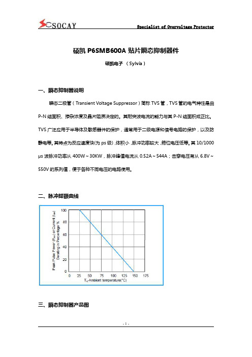
硕凯P6SMB600A贴片瞬态抑制器件硕凯电子(Sylvia)一、瞬态抑制器说明瞬态二极管(Transient Voltage Suppressor)简称TVS管,TVS管的电气特性是由P-N结面积、掺杂浓度及晶片阻质决定的。
其耐突波电流的能力与其P-N结面积成正比。
TVS广泛应用于半导体及敏感器件的保护,通常用于二级电源和信号电路的保护,以及防静电等。
其特点为反应速度快(为ps级),体积小,脉冲功率较大,箝位电压低等。
其10/1000μs波脉冲功率从400W~30KW,脉冲峰值电流从0.52A~544A;击穿电压有从6.8V~550V的系列值,便于各种不同电压的电路使用。
二、脉冲降额曲线三、瞬态抑制器产品图四、产品特性1、为表面安装应用优化电路板空间2、低泄漏3、单向和双向单元4、玻璃钝化结5、低电感6、优良的钳位能力7、600W的峰值功率能力在10×1000μ波形重复率(占空比):0.01%8、快速响应时间:从0伏特到最小击穿电压通常小于1.0ps9、典型的,在电压高于12V时,反向漏电流小于5μA10、高温焊接:终端260°C/40秒11、典型的最大温度系数△Vbr=0.1%x Vbr@25°C x△T12、塑料包装有保险商实验室可燃性94V-013、无铅镀雾锡14、无卤化,符合RoHS15、典型失效模式是在指定的电压或电流下出现16、晶须测试是基于JEDEC JESD201A每个表4a及4c进行的17、IEC-61000-4-2ESD15kV(空气),8kV(接触)18、数据线的ESD保护符合IEC61000-4-2(IEC801-2)19、数据线的EFT保护符合IEC61000-4-4(IEC801-4)五、编带和卷盘说明六、环境规定七、最大额定值Notes:1.Non-repetitive current pulse,per Fig.3and derated above TA=25°C per Fig.2.2.Mounted on5.0mm x5.0mm(0.03mm thick)Copper Pads to each terminal.3.8.3ms single half sine-wave,or equivalent square wave,Duty cycle=4pulses per minutes maximum.4.VF<3.5V for VBR<200V and VF<6.5V for VBR>201V.八、功能线路图九、英文描述The P6SMB series is designed specifically to protect sensitive electronic equipment from voltage transients induced by lightning and other transient voltage events.十、I-V曲线特性十一、产品应用TVS器件非常适合保护I/O接口,Vcc总线和其他应用于电信、计算机、工业和消费电子应用的易损电路。

P6SMB11CAT3 Series600 Watt Peak Power Zener Transient Voltage Suppressors Bidirectional*The SMB series is designed to protect voltage sensitive components from high voltage, high energy transients. They have excellent clamping capability, high surge capability, low zener impedance and fast response time. The SMB series is supplied in ON Semiconductor’s exclusive, cost-effective, highly reliable Surmetic t package and is ideally suited for use in communication systems, automotive, numerical controls, process controls, medical equipment, business machines, power supplies and many other industrial/consumer applications.Features•Working Peak Reverse V oltage Range − 9.4 to 77.8 V •Standard Zener Breakdown V oltage Range − 11 to 91 V •Peak Power − 600 W @ 1 ms•ESD Rating of Class 3 (>16 KV) per Human Body Model •Maximum Clamp V oltage @ Peak Pulse Current•Low Leakage < 5 m A Above 10 V•UL 497B for Isolated Loop Circuit Protection •Response Time is Typically < 1 ns•Pb−Free Packages are AvailableMechanical Characteristics:CASE:V oid-Free, Transfer-Molded, Thermosetting Plastic FINISH:All External Surfaces are Corrosion Resistant and Leads are Readily SolderableMAXIMUM CASE TEMPERATURE FOR SOLDERING PURPOSES: 260°C for 10 SecondsLEADS:Modified L−Bend Providing More Contact Area to Bond Pads POLARITY:Polarity Band Will Not be IndicatedMOUNTING POSITION:AnyMAXIMUM RATINGSRating Symbol Value Unit Peak Power Dissipation (Note 1) @ T L = 25°C,Pulse Width = 1 msP PK600WDC Power Dissipation @ T L = 75°C Measured Zero Lead Length (Note 2) Derate Above 75°CThermal Resistance, Junction−to−LeadP DR q JL3.04025WmW/°C°C/WDC Power Dissipation (Note 3) @ T A = 25°C Derate Above 25°CThermal Resistance, Junction−to−AmbientP DR q JA0.554.4226WmW/°C°C/WOperating and Storage Temperature Range T J, Tstg−65 to+150°CStresses exceeding Maximum Ratings may damage the device. Maximum Ratings are stress ratings only. Functional operation above the Recommended Operating Conditions is not implied. Extended exposure to stresses above the Recommended Operating Conditions may affect device reliability.1.10 X 1000 m s, non−repetitive2.1″ square copper pad, FR−4 board3.FR−4 board, using ON Semiconductor minimum recommended footprint, asshown in 403A case outline dimensions spec.*Please see P6SMB6.8AT3 to P6SMB200AT3 for Unidirectional devices.Devices listed in bold, italic are ON Semiconductor Preferred devices. Preferred devices are recommended choices for future use and best overall value.Device Package Shipping†ORDERING INFORMATIONP6SMBxxCAT3SMB2500/T ape & ReelP6SMBxxCAT3G SMB(Pb−Free)2500/T ape & Reel†For information on tape and reel specifications, including part orientation and tape sizes, please refer to our T ape and Reel Packaging Specifications Brochure, BRD8011/D.The “T3” suffix refers to a 13 inch reel.ELECTRICAL CHARACTERISTICS(T A = 25°C unless otherwise noted)Symbol ParameterI PP Maximum Reverse Peak Pulse CurrentV C Clamping Voltage @ I PPV RWM Working Peak Reverse VoltageI R Maximum Reverse Leakage Current @ V RWMV BR Breakdown Voltage @ I TI T Test CurrentQ V BR Maximum Temperature Coefficient of V BRELECTRICAL CHARACTERISTICS (Devices listed in bold, italic are ON Semiconductor Preferred devices.)Device*DeviceMarkingV RWM(Note 4)I R@V RWMBreakdown Voltage V C @ I PP(Note 6)Q V BRC typ(Note 7)V BR Volts (Note 5)@ I T V C I PPVolts m A Min Nom Max mA Volts Amps%/°C pFP6SMB11CAT3, G P6SMB12CAT3, G P6SMB13CAT3, G 11C12C13C9.410.211.155510.511.412.411.051213.0511.612.613.711115.616.718.23836330.0750.0780.081865800740P6SMB15CAT3, G P6SMB16CAT3, G P6SMB18CAT3, G P6SMB20CAT3, G 15C16C18C20C12.813.615.317.1555514.315.217.11915.0516182015.816.818.921111121.222.525.227.7282724220.0840.0860.0880.09645610545490P6SMB22CAT3, G P6SMB24CAT3, G P6SMB27CAT3, G P6SMB30CAT3, G 22C24C27C30C18.820.523.125.6555520.922.825.728.5222427.053023.125.228.431.5111130.633.237.541.420181614.40.090.0940.0960.097450415370335P6SMB33CAT3, G P6SMB36CAT3, G P6SMB39CAT3, G P6SMB43CAT3, G 33C36C39C43C28.230.833.336.8555531.434.237.140.933.053639.0543.0534.737.84145.2111145.749.953.959.313.21211.210.10.0980.0990.10.101305280260240P6SMB47CAT3, G P6SMB51CAT3, G P6SMB56CAT3, G P6SMB62CAT3, G 47C51C56C62C40.243.647.853555544.748.553.258.947.0551.05566249.453.658.865.1111164.870.177859.38.67.87.10.1010.1020.1030.104220205185170P6SMB68CAT3, G P6SMB75CAT3, G P6SMB82CAT3, G P6SMB91CAT3, G 68C75C82C91C58.164.170.177.8555564.671.377.986.56875.05829171.478.886.195.51111921031131256.55.85.34.80.1040.1050.1050.1061551401301204. A transient suppressor is normally selected according to the working peak reverse voltage (V RWM), which should be equal to or greater thanthe DC or continuous peak operating voltage level.5.V BR measured at pulse test current I T at an ambient temperature of 25°C.6.Surge current waveform per Figure 2 and derate per Figure 3 of the General Data − 600 Watt at the beginning of this group.7.Bias Voltage = 0 V, F = 1 MHz, T J = 25°C*The “G’’ suffix indicates Pb−Free package available. Please refer back to Ordering Information on front page.P , P E A K P O W E R (k W )P 1101000.1t, TIME (ms)Figure 2. Pulse WaveformTYPICAL PROTECTION CIRCUITFigure 3. Pulse Derating CurveP E A K P U L S E D E R A T I N G I N % O F P E A K P O W E R O R C U R R E N T @ T A = 25C°T A , AMBIENT TEMPERATURE (°C)Figure 4. Typical Junction Capacitance vs. BiasVoltageBIAS VOLTAGE (VOLTS)110100C , C A P A C I T A N C E (p F )APPLICATION NOTESRESPONSE TIMEIn most applications, the transient suppressor device is placed in parallel with the equipment or component to be protected. In this situation, there is a time delay associated with the capacitance of the device and an overshoot condition associated with the inductance of the device and the inductance of the connection method. The capacitive effect is of minor importance in the parallel protection scheme because it only produces a time delay in the transition from the operating voltage to the clamp voltage as shown in Figure 4.The inductive effects in the device are due to actual turn-on time (time required for the device to go from zero current to full current) and lead inductance. This inductive effect produces an overshoot in the voltage across the equipment or component being protected as shown in Figure 5. Minimizing this overshoot is very important in the application, since the main purpose for adding a transient suppressor is to clamp voltage spikes. The SMB series have a very good response time, typically < 1 ns and negligible inductance. However, external inductive effects could produce unacceptable overshoot. Proper circuit layout, minimum lead lengths and placing the suppressor device as close as possible to the equipment or components to be protected will minimize this overshoot. Some input impedance represented by Z in is essential to prevent overstress of the protection device. This impedance should be as high as possible, without restricting the circuit operation.DUTY CYCLE DERATINGThe data of Figure 1 applies for non-repetitive conditions and at a lead temperature of 25°C. If the duty cycle increases, the peak power must be reduced as indicated by the curves of Figure 6. A verage power must be derated as the lead or ambient temperature rises above 25°C. The average power derating curve normally given on data sheets may be normalized and used for this purpose.At first glance the derating curves of Figure 6 appear to be in error as the 10 ms pulse has a higher derating factor than the 10 m s pulse. However, when the derating factor for a given pulse of Figure 6 is multiplied by the peak power value of Figure 1 for the same pulse, the results follow the expected trend.VFigure 5. Figure 6.Figure 7. Typical Derating Factor for Duty CycleD E R A T I N GF A C T O R10.70.50.30.050.10.010.020.030.07D, DUTY CYCLE (%)UL RECOGNITIONThe entire series has Underwriters Laboratory Recognition for the classification of protectors (QVGV2)under the UL standard for safety 497B and File #116110.Many competitors only have one or two devices recognized or have recognition in a non-protective category. Some competitors have no recognition at all. With the UL497B recognition, our parts successfully passed several testsincluding Strike V oltage Breakdown test, Endurance Conditioning, Temperature test, Dielectric V oltage-Withstand test, Discharge test and several more.Whereas, some competitors have only passed a flammability test for the package material, we have been recognized for much more to be included in their Protector category.PACKAGE DIMENSIONSSMBDO−214AACASE 403A−03ISSUE F*For additional information on our Pb−Free strategy and solderingdetails, please download the ON Semiconductor Soldering andMounting Techniques Reference Manual, SOLDERRM/D.SURMETIC is a trademark of Semiconductor Components Industries, LLC.ON Semiconductor and are registered trademarks of Semiconductor Components Industries, LLC (SCILLC). SCILLC reserves the right to make changes without further notice to any products herein. SCILLC makes no warranty, representation or guarantee regarding the suitability of its products for any particular purpose, nor does SCILLC assume any liability arising out of the application or use of any product or circuit, and specifically disclaims any and all liability, including without limitation special, consequential or incidental damages.“Typical” parameters which may be provided in SCILLC data sheets and/or specifications can and do vary in different applications and actual performance may vary over time. All operating parameters, including “Typicals” must be validated for each customer application by customer’s technical experts. SCILLC does not convey any license under its patent rights nor the rights of others. SCILLC products are not designed, intended, or authorized for use as components in systems intended for surgical implant into the body, or other applications intended to support or sustain life, or for any other application in which the failure of the SCILLC product could create a situation where personal injury or death may occur. Should Buyer purchase or use SCILLC products for any such unintended or unauthorized application, Buyer shall indemnify and hold SCILLC and its officers, employees, subsidiaries, affiliates, and distributors harmless against all claims, costs, damages, and expenses, and reasonable attorney fees arising out of, directly or indirectly, any claim of personal injury or death associated with such unintended or unauthorized use, even if such claim alleges that SCILLC was negligent regarding the design or manufacture of the part. SCILLC is an Equal Opportunity/Affirmative Action Employer. This literature is subject to all applicable copyright laws and is not for resale in any manner.PUBLICATION ORDERING INFORMATION。


PB-08482-001_v02 | August 2017 Product BriefDOCUMENT CHANGE HISTORYPB-08482-001_v02Version Date Authors Description of Change01 March 24, 2017 VK, DV Initial release02 August 31, 2017 VK, DV Removed NVIDIA Confidential informationTABLE OF CONTENTS Overview (1)Specifications (3)Product Specification (3)Design Discussion (5)Form Factor (5)MXM PCB Mounting Holes (6)Compute Mode (8)Support Information (9)Certificates and Agencies (9)Certifications (9)Agencies (9)LIST OF FIGURES Figure 1. Tesla P6 Board (2)Figure 2. Tesla P6 Board Outline (5)Figure 3. Mounting Holes (6)LIST OF TABLES Table 1. Product Specifications (3)Table 2. Memory Specifications (4)Table 3. Software Feature Specifications (4)Table 4. Thermal Specifications (4)Table 5. Tesla P6 Board Outline Specifications (6)Table 6. Mounting Holes Specifications (7)Table 7. Compute Mode Settings (8)The NVIDIA® Tesla® P6 is an MXM 3.1 Type B card with a single NVIDIA® Pascal™GP104 graphics processing unit (GPU). It has 16 GB GDDR5 video memory and a 90 Watt maximum power limit.This board is intended for accelerated graphics in virtual remote workstation and virtual desktop environments, as well as for single precision GPU compute tasks. Tesla P6 is specifically optimized for space constrained systems like blade servers.NVIDIA does not ship this board with a cooling solution attached, however NVIDIA does provide thermal specifications for OEMs to design their custom heat sinks.A main feature of the Tesla P6 board is the support of NVIDIA® GRID™ software which includes NVIDIA® GRID™ vGPU™. This technology enables the virtualization of physical GPUs into full-featured virtual GPUs providing maximum performance and scalability.For performance optimization, this board utilizes NVIDIA GPU BOOST™. By adjusting the GPU clock dynamically, maximum performance is achieved within the power cap limit (90 W).Tesla P6 supports H.264 and H.265 hardware encoding, which is particularly important for reducing round-trip latency and image quality for virtual desktops and applications.OverviewFigure 1. Tesla P6 BoardPRODUCT SPECIFICATIONTable 1 provides the product specifications for the Tesla P6 board. Table 1. Product SpecificationsSpecification DescriptionBoard SKU PG418 SKU 200Total board power 90 W (70 W optional)GPU SKU GP104-995IDs DEVID: 0x1BB4SSID: 0x11C6Form Factor MXM 3.1 Type BNVIDIA® CUDA® cores 2048GPU clocks Base 1012 MHz (TGP: 90 W) Boost 1506 MHz (TGP: 90 W)PCI Express interface P0: Gen3 16 lanes, 16.0 GbpsP8: Gen1 16 lanes, 2.5 GbpsSpecificationsTable 2 provides the memory specifications for the Tesla P6 graphics board.Table 2. Memory SpecificationsSpecification DescriptionMemory clock 3003 MHzMemory size 16 GBMemory I/O 256-bitMemory configuration 16 pcs 256M × 16 GDDR5sMemory bandwidth 192.2 GB/sTable 3 provides the software feature specifications.Table 3. Software Feature SpecificationsSpecification DescriptionEEPROM size 4 Mb Serial ROMPCI class code PCI base class: 0x03PCI sub-class: 0x02ECC support Supported (enabled by default)SMBPBI (SMBus Post Box Interface) SupportedTable 4 provides the thermal specifications for the Tesla P6 graphics board.Table 4. Thermal SpecificationsAction T j (°C)GPU shutdown temperature 94GPU slowdown temperature 91GPU maximum operating temperature 89GPU hardware slowdown amount 50%FORM FACTORTesla P6 follows the MXM 3.1 Type B mechanical specifications. For more details on the mechanical specifications, refer to the latest version of the MXM Electromechanical Specification.Figure 2. Tesla P6 Board OutlineTable 5. Tesla P6 Board Outline SpecificationsSymbolmm inchesMinimum Nominal Maximum Minimum Nominal MaximumA1 82.00 3.228A2 70.00 2.756A3 105.00 4.134A4 3.37 3.50 3.63 0.133 0.138 0.143A5 78.37 78.50 78.63 3.085 3.091 3.096A6 3.87 4.00 4.13 0.152 0.157 0.163A7 65.87 66.00 66.13 2.593 2.598 2.604A8 38.87 39.00 39.13 1.530 1.535 1.541MXM PCB MOUNTING HOLESThe module has six holes. Two are used to secure the board to the system and the other four to fasten the thermal solution to the module.Figure 3. Mounting HolesTable 6. Mounting Holes SpecificationsSymbolmm inchesMinimum Nominal Maximum Minimum Nominal MaximumB1 75.00 2.953B2 8.25 0.325B3 54.25 2.136B4 5.50 0.217B5 51.50 2.028B6 3.07 3.20 3.33 0.121 0.126 0.131 B7 3.07 3.20 3.33 0.121 0.126 0.131In contrast to Tesla M6, Tesla P6 is offered only in compute mode. Starting with Pascal-generation boards, switching between graphics and compute mode is no longerrequired. NVIDIA GRID software automatically handles most setting adjustments previously requiring the switch to graphics mode. Nevertheless, ECC must be disabledbefore running NVIDIA GRID software.Table 7 provides details of the compute mode settings.Table 7. Compute Mode SettingsSetting Value NotesClass code 3D Controller This class code indicates to operatingsystems (OS) that the GPU is not intendedfor use as a primary display device. Memory BAR 16 gigabytes Tesla GPUs expose a large memory baseaddress register (BAR) for direct access tothe frame buffer from the CPU, and otherPCI Express devices.I/O base BAR Disabled The GPU need not consume any legacy I/Oresources when used as a non-displaydevice.ECC protection Enabled Error Correcting Code (ECC) is enabled onthe GPU frame buffer to protect againstsingle- and multi-bit memory errors. ECCcan be turned off.CERTIFICATES AND AGENCIESCertifications④Windows Hardware Quality Lab (WHQL):●Certified Windows 7, Windows 8.1, and Windows 10●Certified Windows Server 2008 R2, Windows Server 2012 R2, and Windows Server2016④EU Reduction of Hazardous Substances (EU RoHS)④Joint Industry guide (J-STD) / Registration, Evaluation, Authorization, and Restriction of Chemical Substance (EU) – (JIG / REACH)④Halogen Free (HF)④EU Waste Electrical and Electronic Equipment (WEEE)Agencies④Australian Communications Authority and Radio Spectrum Management Group of New Zealand (C-Tick)④Bureau of Standards, Metrology, and Inspection (BSMI)④Conformité Européenne (CE)④Federal Communications Commission (FCC)④Industry Canada - Interference-Causing Equipment Standard (ICES)④Underwriters Laboratories (cUL, UL)④Voluntary Control Council for Interference (VCCI)NoticeThe information provided in this specification is believed to be accurate and reliable as of the date provided. However, NVIDIA Corporation (“NVIDIA”) does not give any representations or warranties, expressed or implied, as to the accuracy or completeness of such information. NVIDIA shall have no liability for the consequences or use of such information or for any infringement of patents or other rights of third parties that may result from its use. This publication supersedes and replaces all other specifications for the product that may have been previously supplied.NVIDIA reserves the right to make corrections, modifications, enhancements, improvements, and other changes to this specification, at any time and/or to discontinue any product or service without notice. Customer should obtain the latest relevant specification before placing orders and should verify that such information is current and complete.NVIDIA products are sold subject to the NVIDIA standard terms and conditions of sale supplied at the time of order acknowledgement, unless otherwise agreed in an individual sales agreement signed by authorized representatives of NVIDIA and customer. NVIDIA hereby expressly objects to applying any customer general terms and conditions with regard to the purchase of the NVIDIA product referenced in this specification.NVIDIA products are not designed, authorized or warranted to be suitable for use in medical, military, aircraft, space or life support equipment, nor in applications where failure or malfunction of the NVIDIA product can reasonably be expected to result in personal injury, death or property or environmental damage. NVIDIA accepts no liability for inclusion and/or use of NVIDIA products in such equipment or applications and therefore such inclusion and/or use is at customer’s own risk.NVIDIA makes no representation or warranty that products based on these specifications will be suitable for any specified use without further testing or modification. Testing of all parameters of each product is not necessarily performed by NVIDIA. It is customer’s sole responsibility to ensure the product is suitable and fit for the application planned by customer and to do the necessary testing for the application in order to avoid a default of the application or the product. Weaknesses in customer’s product designs may affect the quality and reliability of the NVIDIA product and may result in additional or different conditions and/or requirements beyond those contained in this specification. NVIDIA does not accept any liability related to any default, damage, costs or problem which may be based on or attributable to: (i) the use of the NVIDIA product in any manner that is contrary to this specification, or (ii) customer product designs.No license, either expressed or implied, is granted under any NVIDIA patent right, copyright, or other NVIDIA intellectual property right under this specification. Information published by NVIDIA regarding third-party products or services does not constitute a license from NVIDIA to use such products or services or a warranty or endorsement thereof. Use of such information may require a license from a third party under the patents or other intellectual property rights of the third party, or a license from NVIDIA under the patents or other intellectual property rights of NVIDIA. Reproduction of information in this specification is permissible only if reproduction is approved by NVIDIA in writing, is reproduced without alteration, and is accompanied by all associated conditions, limitations, and notices.ALL NVIDIA DESIGN SPECIFICATIONS, REFERENCE BOARDS, FILES, DRAWINGS, DIAGNOSTICS, LISTS, AND OTHER DOCUMENTS (TOGETHER AND SEPARATELY, “MATERIALS”) ARE BEING PROVIDED “AS IS.” NVIDIA MAKES NO WARRANTIES, EXPRESSED, IMPLIED, STATUTORY, OR OTHERWISE WITH RESPECT TO THE MATERIALS, AND EXPRESSLY DISCLAIMS ALL IMPLIED WARRANTIES OF NONINFRINGEMENT, MERCHANTABILITY, AND FITNESS FOR A PARTICULAR PURPOSE. Notwithstanding any damages that customer might incur for any reason whatsoever, NVIDIA’s aggregate and cumulative liability towards customer for the products described herein shall be limited in accordance with the NVIDIA terms and conditions of sale for the product.TrademarksNVIDIA, the NVIDIA logo, BOOST, CUDA, GRID, Pascal, and Tesla are trademarks and/or registered trademarks of NVIDIA Corporation in the U.S. and other countries. Other company and product names may be trademarks of the respective companies with which they are associated.Copyright© 2017 NVIDIA Corporation. All rights reserved.。

MECHANICAL DATACase: SMB (DO-214AA)Molding compound meets UL 94 V-0 flammability rating Base P/N-E3 - RoHS-compliant, commercial gradeBase P/N-M3 - halogen-free, RoHS-compliant, commercial gradeBase P/NHE3_X - RoHS-compliant and AEC-Q101 qualified Base P/NHM3_X - halogen-free, RoHS-compliant, and AEC-Q101 qualified(“_X” denotes revision code e.g. A, B, ..... and only available for 250 V to 540 V type)Terminals: matte tin plated leads, solderable per J-STD-002 and JESD 22-B102E3, M3, HE3, and HM3 suffix meets JESD 201 class 2 whisker testPolarity: for uni-directional types the band denotes cathode end, no marking on bi-directional typesNotes(1) Non-repetitive current pulse, per fig. 3 and derated above T A= 25 °C per fig. 2 (2) Mounted on 0.2" x 0.2" (5.0 mm x 5.0 mm) copper pads to each terminalFEATURES• Low profile package• Ideal for automated placement • Glass passivated chip junction• Available in uni-directional and bi-directional • 600 W peak pulse power capability with a 10/1000 μs waveform, repetitive rate (duty cycle): 0.01 %• Excellent clamping capability • Very fast response time• Low incremental surge resistance• Meets MSL level 1, per J-STD-020, LF maximum peak of 260 °C• AEC-Q101 qualified available- Automotive ordering code: base P/NHE3 or P/NHM3(1) Pulse test: t p 50 ms(2) Surge current waveform per fig. 3 and derate per fig. 2(3) For bi-directional types with V WM of 10 V and less, the I D limit is doubled(4) All terms and symbols are consistent with ANSI/IEEE CA62.35(5) V F = 3.5 V at I F = 50 A (uni-directional only)RATINGS AND CHARACTERISTICS CURVES (T A = 25 °C unless otherwise noted)1001011007550250.10.1 µs 1.0 µs 10 µs 100 µs 1.0 ms 10 ms0 25 50 75 100125 150 175 200t d - Pulse Width (s) TJ - Initial Temperature (°C) Fig. 1 - Peak Pulse Power Rating Curve Fig. 2 - Pulse Power or Current vs. Initial Junction TemperatureFig. 3 - Pulse Waveform Fig. 5 - Typical Transient Thermal Impedance Fig. 4 - Typical Junction Capacitance Fig. 6 - Maximum Non-Repetitive Peak Forward Surge Current PPPM-PeakPulsePower(kW)PeakPulsePower(PPP)orCurrent(IPP)DeratinginPercentage,%。

P6SMBJ SERIESSURFACE MOUNT TRANSIENT VOLTAGE SUPPRESSOR VOLTAGE - 5.0 TO 170 Volts Peak Power Pulse - 600WattFEATURESl For surface mounted applications in order to optimize board space l Low profile package l Built-in strain relief l Glass passivated junction l Low inductancel Excellent clamping capability l Repetition Rate(duty cycle):0.01% l Fast response time: typically less than 1.0 ps from 0 volts to BV for unidirectional types l Typical I D less than 1 A above 10V l High temperature soldering : 260 /10 seconds at terminalsl Plastic package has Underwriters Laboratory Flammability Classification 94V-OMECHANICAL DATACase: JEDEC DO-214AA molded plastic over passivated junctionTerminals: Solder plated, solderable per MIL-STD-750, Method 2026Polarity: Color band denotes positive end(cathode) except BidirectionalStandard packaging:12 mm tape per(EIA 481) Weight: 0.003 ounce, 0.093 gramMAXIMUM RATINGS AND ELECTRICAL CHARACTERISTICSRatings at 25 ambient temperature unless otherwise specified.SYMBOL VALUEUNITS Peak Pulse Power Dissipation on 10/1000 s waveform (Note 1,2,Fig 1)P PPM Minimum 600 Watts Peak Pulse Current on 10/1000 s waveform (Note 1,Fig 3)I PPM See Table 1 Amps Peak forward Surge Current 8.3ms single half sine-wave superimposed on rated load(JEDEC Method) (Note 2,3) I FSM 100.0 AmpsOperating Junction and Storage Temperature Range T J ,T STG-55 to +150NOTES:1.Non-repetitive current pulse, per Fig. 3 and derated above T A =25 per Fig.2. SMB/DO-214AA查询P6SMBJ14A供应商2.Mounted on 5.0mm2 (.013mm thick) land areas.3.Measured on 8 .3ms, single half sine-wave or equivalent square wave, duty cycle= 4 pulses per minutes maximum.MAXIMUM RATINGS AND CHARACTERISTIC CURVES P6SMBJ SERIESFig. 1-PEAK PULSE POWER RATING VERSUS Fig. 2-PULSE RATING CURVEFig. 3-PULSE WAVEFORM Fig. 4-TYPICAL JUNCTIONCAPACITANCENUMBER VRWM (V) MIN. @IT MAX. @IT (mA) @I PP VC (V) I PP (A) IR (uA)P6SMBJ5.0 P6SMBJ5.0A P6SMBJ6.0 P6SMBJ6.0A KDKEKFKG5.05.06.06.06.406.406.676.677.557.258.457.67101010109.69.211.410.362.565.252.658.3800800800800P6SMBJ6.5 P6SMBJ6.5A P6SMBJ7.0 P6SMBJ7.0A KHKKKLKM6.56.57.07.07.227.227.787.789.148.309.868.951010101012.311.213.312.048.753.645.150.0500500200200P6SMBJ7.5 P6SMBJ7.5A P6SMBJ8.0 P6SMBJ8.0A KNKPKQKR7.57.58.08.08.338.338.898.8910.679.5811.3010.23111114.312.915.013.642.046.540.044.11001005050P6SMBJ8.5 P6SMBJ8.5A P6SMBJ9.0 P6SMBJ9.0A KSKTKUKV8.58.59.09.09.449.4410.0010.0011.9210.8212.6011.50111115.914.416.915.437.741.735.539.0101055P6SMBJ10 P6SMBJ10A P6SMBJ11 P6SMBJ11A KWKXKYKZ10.010.011.011.011.1011.1012.2012.2014.1012.8015.4014.00111118.817.020.118.231.935.329.933.05555P6SMBJ12 P6SMBJ12A P6SMBJ13 P6SMBJ13A LDLELFLG12.012.013.013.013.3013.3014.4014.4016.9015.3018.2016.50111122.019.923.821.527.330.225.227.95555P6SMBJ14 P6SMBJ14A P6SMBJ15 P6SMBJ15A LHLKLLLM14.014.015.015.015.6015.6016.7016.7019.8017.9021.1019.20111125.823.226.924.423.325.822.324.05555P6SMBJ16 P6SMBJ16A P6SMBJ17 P6SMBJ17A LNLPLQLR16.016.017.017.017.8017.8018.9018.9022.6020.5023.9021.70111128.826.030.527.620.823.119.721.75555P6SMBJ18 P6SMBJ18A P6SMBJ20 P6SMBJ20A LSLTLULV18.018.020.020.020.0020.0022.2022.2025.3023.3028.1025.50111132.229.235.832.418.620.516.718.55555P6SMBJ22 P6SMBJ22A P6SMBJ24 P6SMBJ24A LWLXLYLZ22.022.024.024.024.4024.4026.7026.7030.9028.0033.8030.70111139.435.543.038.915.216.914.015.45555P6SMBJ26 P6SMBJ26A P6SMBJ28 P6SMBJ28A MDMEMFMG26.026.028.028.028.9028.9031.1031.1036.6033.2039.4035.80111146.642.150.045.412.414.212.013.25555P6SMBJ30 P6SMBJ30A P6SMBJ33 P6SMBJ33A MHMKMLMM30.030.033.033.033.3033.3036.7036.7042.2038.3046.5042.20111153.548.459.053.311.212.410.211.35555P6SMBJ36 P6SMBJ36A P6SMBJ40 P6SMBJ40A MNMPMQMR36.036.040.040.040.0040.0044.4044.4050.7046.0056.3051.10111164.358.171.464.59.310.38.49.35555P6SMBJ43 P6SMBJ43A P6SMBJ45 P6SMBJ45A MSMTMUMV43.043.045.045.047.8047.8050.0050.0060.5054.9063.3057.50111176.769.480.372.77.88.67.58.35555P6SMBJ48 P6SMBJ48A P6SMBJ51 P6SMBJ51A MWMXMYMZ48.048.051.051.053.3053.3056.7056.7067.5061.3071.8065.20111185.577.491.182.47.07.76.67.35555P6SMBJ54 P6SMBJ54A P6SMBJ58 P6SMBJ58A NDNENFNG54.054.058.058.060.0060.0064.4064.4076.0069.0081.6074.10111196.387.1103.093.66.26.95.86.45555P6SMBJ60 P6SMBJ60A P6SMBJ64 P6SMBJ64A NHNKNLNM60.060.064.064.066.7066.7071.1071.1084.5076.7090.1081.801111107.096.8114.0103.05.66.25.35.85555NUMBER VRWM (V) MIN. @IT MAX. @IT (mA) @I PP VC (V) I PP (A) IR (uA)P6SMBJ70 P6SMBJ70A P6SMBJ75 P6SMBJ75A NNNPNQNR70.070.075.075.077.8077.8083.3083.3098.6089.50105.7095.801111125.0113.0134.0121.04.85.34.54.95555P6SMBJ78 P6SMBJ78A P6SMBJ85 P6SMBJ85A NSNTNUNV78.078.085.085.086.7086.7094.4094.40109.8099.70119.20108.201111139.0126.0151.0137.04.34.73.94.45555P6SMBJ90P6SMBJ90A P6SMBJ100 P6SMBJ100A NWNXNYNZ90.090.0100.0100.0100.00100.00111.00111.00126.50115.50141.00128.001111160.0146.0179.0162.03.84.13.43.75555P6SMBJ110 P6SMBJ110A P6SMBJ120 P6SMBJ120A PDPEPFPG110.0110.0120.0120.0122.00122.00133.00133.00154.50140.50169.00153.001111196.0177.0214.0193.03.03.42.83.15555P6SMBJ130 P6SMBJ130A P6SMBJ150 P6SMBJ150A PHPKPLPM130.0130.0150.0150.0144.00144.00167.00167.00182.50165.50211.50192.501111231.0209.0268.0243.02.62.92.22.55555P6SMBJ160 P6SMBJ160A P6SMBJ170 P6SMBJ170A PNPPPQPR160.0160.0170.0170.0178.00178.00189.00189.00226.00205.00239.50217.501111287.0259.0304.0275.02.12.32.02.25555BI-DIRECTIONAL 600 Watt Surface Mount TVSBI-DIRECTIONALPARTNUMBERDEVICEMARKINGCODEREVERSESTAND-OFFVOLTAGEVRWM (V)BREAKDOWNVOLTAGEVBR (V)MIN. @ITBREAKDOWNVOLTAGEVBR (V)MAX. @ITTESTCURRENTIT(mA)MAXIMUMCLAMPINGVOLTAGE@I PP VC (V)PEAKPULSECURRENTI PP (A)REVERSELEAKAGE@VRWMIR (uA)P6SMBJ5.0C P6SMBJ5.0CA P6SMBJ6.0C P6SMBJ6.0CA ADAEAFAG5.05.06.06.06.406.406.676.677.557.258.457.67101010109.69.211.410.362.565.252.658.31600160016001600P6SMBJ6.5C P6SMBJ6.5CA P6SMBJ7.0C P6SMBJ7.0CA AHAKALAM6.56.57.07.07.227.227.787.789.148.309.868.951010101012.311.213.312.048.753.645.150.010001000400400P6SMBJ7.5C P6SMBJ7.5CA P6SMBJ8.0C P6SMBJ8.0CA ANAPAQAR7.57.58.08.08.338.338.898.8910.679.5811.3010.23111114.312.915.013.642.046.540.044.1200200100100P6SMBJ8.5C P6SMBJ8.5CA P6SMBJ9.0C P6SMBJ9.0CA ASATAUAV8.58.59.09.09.449.4410.0010.0011.9210.8212.6011.50111115.914.416.915.437.741.735.539.020201010P6SMBJ10C P6SMBJ10CA P6SMBJ11C P6SMBJ11CA AWAXAYAZ10.010.011.011.011.1011.1012.2012.2014.1012.8015.4014.00111118.817.020.118.231.935.329.933.05555P6SMBJ12C P6SMBJ12CA P6SMBJ13C P6SMBJ13CA BDBEBFBG12.012.013.013.013.3013.3014.4014.4016.9015.3018.2016.50111122.019.923.821.527.330.225.227.95555P6SMBJ14C P6SMBJ14CA P6SMBJ15C P6SMBJ15CA BHBKBLBM14.014.015.015.015.6015.6016.7016.7019.8017.9021.1019.20111125.823.226.924.423.325.822.324.05555P6SMBJ16C P6SMBJ16CA P6SMBJ17C P6SMBJ17CA BNBPBQBR16.016.017.017.017.8017.8018.9018.9022.6020.5023.9021.70111128.826.030.527.620.823.119.721.75555P6SMBJ18C P6SMBJ18CA P6SMBJ20C P6SMBJ20CA BSBTBUBV18.018.020.020.020.0020.0022.2022.2025.3023.3028.1025.50111132.229.235.832.418.620.516.718.55555P6SMBJ22C P6SMBJ22CA P6SMBJ24C P6SMBJ24CA BWBXBYBZ22.022.024.024.024.4024.4026.7026.7030.9028.0033.8030.70111139.435.543.038.915.216.914.015.45555P6SMBJ26C P6SMBJ26CA CDCE26.026.028.9028.9036.6033.201146.642.112.414.255P6SMBJ28C P6SMBJ28CA CFCG28.028.031.1031.1039.4035.801150.045.412.013.255P6SMBJ30C P6SMBJ30CA P6SMBJ33C P6SMBJ33CA CHCKCLCM30.030.033.033.033.3033.3036.7036.7042.2038.3046.5042.20111153.548.459.053.311.212.410.211.35555P6SMBJ36C P6SMBJ36CA P6SMBJ40C P6SMBJ40CA CNCPCQCR36.036.040.040.040.0040.0044.4044.4050.7046.0056.3051.10111164.358.171.464.59.310.38.49.35555P6SMBJ43C P6SMBJ43CA P6SMBJ45C P6SMBJ45CA CSCTCUCV43.043.045.045.047.8047.8050.0050.0060.5054.9063.3057.50111176.769.480.372.77.88.67.58.35555P6SMBJ48C P6SMBJ48CA P6SMBJ51C P6SMBJ51CA CWCXCYCZ48.048.051.051.053.3053.3056.7056.7067.5061.3071.8065.20111185.577.491.182.47.07.76.67.35555P6SMBJ54C P6SMBJ54CA P6SMBJ58C P6SMBJ58CA DDDEDFDG54.054.058.058.060.0060.0064.4064.4076.0069.0081.6074.10111196.387.1103.093.66.26.95.86.45555P6SMBJ60C P6SMBJ60CA P6SMBJ64C P6SMBJ64CA DHDKDLDM60.060.064.064.066.7066.7071.1071.1084.5076.7090.1081.801111107.096.8114.0103.05.66.25.35.85555BI-DIRECTIONAL 600 Watt Surface Mount TVSBI-DIRECTIONALPARTNUMBERDEVICEMARKINGCODEREVERSESTAND-OFFVOLTAGEVRWM (V)BREAKDOWNVOLTAGEVBR (V)MIN. @ITBREAKDOWNVOLTAGEVBR (V)MAX. @ITTESTCURRENTIT(mA)MAXIMUMCLAMPINGVOLTAGE@I PP VC (V)PEAKPULSECURRENTI PP (A)REVERSELEAKAGE@VRWMIR (uA)P6SMBJ70C P6SMBJ70CA P6SMBJ75C P6SMBJ75CA DNDPDQDR70.070.075.075.077.8077.8083.3083.3098.6089.50105.7095.801111125.0113.0134.0121.04.85.34.54.95555P6SMBJ78C P6SMBJ78CA P6SMBJ85C P6SMBJ85CA DSDTDUDV78.078.085.085.086.7086.7094.4094.40109.8099.70119.20108.201111139.0126.0151.0137.04.34.73.94.45555P6SMBJ90CP6SMBJ90CA P6SMBJ100C P6SMBJ100CA DWDXDYDZ90.090.0100.0100.0100.00100.00111.00111.00126.50115.50141.00128.001111160.0146.0179.0162.03.84.13.43.75555P6SMBJ110C P6SMBJ110CA P6SMBJ120C P6SMBJ120CA EDEEEFEG110.0110.0120.0120.0122.00122.00133.00133.00154.50140.50169.00153.001111196.0177.0214.0193.03.03.42.83.15555P6SMBJ130C P6SMBJ130CA P6SMBJ150C P6SMBJ150CA EHEKELEM130.0130.0150.0150.0144.00144.00167.00167.00182.50165.50211.50192.501111231.0209.0268.0243.02.62.92.22.55555P6SMBJ160C P6SMBJ160CA P6SMBJ170C P6SMBJ170CA ENEPEQER160.0160.0170.0170.0178.00178.00189.00189.00226.00205.00239.50217.501111287.0259.0304.0275.02.12.32.02.25555。


低功耗瞬态管P6SMB15CA型号说明硕凯电子(Sylvia)一、最大额定值Notes:1.Non-repetitive current pulse,per Fig.3and derated above TA=25°C per Fig.2.2.Mounted on5.0mm x5.0mm(0.03mm thick)Copper Pads to each terminal.3.8.3ms single half sine-wave,or equivalent square wave,Duty cycle=4pulses per minutes maximum.4.VF<3.5V for VBR<200V and VF<6.5V for VBR>201V.二、脉冲浪涌三、UL认证编号四、产品应用说明TVS器件非常适合保护I/O接口,Vcc总线和其他应用于电信、计算机、工业和消费电子应用的易损电路。
五、脉冲降额曲线五、电路图六、I-V曲线特性七、产品特性1、为表面安装应用优化电路板空间2、低泄漏3、单向和双向单元4、玻璃钝化结5、低电感6、优良的钳位能力7、600W的峰值功率能力在10×1000μ波形重复率(占空比):0.01%8、快速响应时间:从0伏特到最小击穿电压通常小于1.0ps9、典型的,在电压高于12V时,反向漏电流小于5μA10、高温焊接:终端260°C/40秒11、典型的最大温度系数△Vbr=0.1%x Vbr@25°C x△T12、塑料包装有保险商实验室可燃性94V-013、无铅镀雾锡14、无卤化,符合RoHS15、典型失效模式是在指定的电压或电流下出现16、晶须测试是基于JEDEC JESD201A每个表4a及4c进行的17、IEC-61000-4-2ESD15kV(空气),8kV(接触)18、数据线的ESD保护符合IEC61000-4-2(IEC801-2)19、数据线的EFT保护符合IEC61000-4-4(IEC801-4)八、瞬态管产品图。


P6SMB600 W Transient voltage suppressorProduct features• Low profile SMB package • Excellent clamping capability•600 W peak pulse power capability at 10/1000 μs waveform• Typical I R less than 1 μA above 12 V•Fast response time: typically less than 1.0 ps from 0 V to V BR minimum•High temperature reflow soldering: +260 °C /40 s at terminal•Plastic package meets UL 94 V-0 flammability rating• Meets moisture sensitivity level (MSL) level 1•Terminal: Solder plated leads, solderable per J-STD-002•For surface mounted applications in order to optimize board space•UL 497B recognized.File No. : E198449 Guide QVGQ2Applications• Consumer electronics • Telecommunications • Computing and servers • Appliances• Industrial automation •Mobile and wearablesEnvironmental compliance and general specificationsP6SMB 6-8 C AFamily name V R voltage(“-” indicates decimal point) Bi-/Uni-Directional(Blank=Uni, C=Bi)Voltage toleranceOrdering part numberPIN configurationPb HALOGENHF FREE2Technical Data 11212Effective November 2020P6SMB600 W Transient voltage suppressor/electronicsParameterSymbolValueUnitStorage operating junction temperature range T STG / T J -55 to +150°C Steady state power dissipation at T L = +75 °C P M(AV) 5.0W Peak pulse power dissipation on 10/1000 μs waveformP PP 600W Maximum instantaneous forward voltage at 100 A for unidirectionalV F 5.0V Peak forward surge current, 8.3 ms single half sine wave 1I FSM 100A Typical thermal resistance junction to leadR JL20°C/W Typical thermal resistance junction to ambientR JA100°C/WAbsolute maximum ratings(+25 °C, RH=45%-75%, unless otherwise noted)1. Measured on 8.3 ms single half sine wave or equivalent square wave for unidirectional device only, duty cycle = 4 per minute maximumPackaging information (mm)Drawing not to scale.Supplied in tape and reel packaging, 3,000 parts per 13” diameter reel (EIA-481 compliant)Mechanical parameters, pad layout- mmMillimetersInches Dimension MinimumMaximumMinimumMaximumA 3.30 3.940.1300.155B 4.30 4.800.1690.189C 1.90 2.200.0750.087D 0.95 1.520.0370.060E 5.20 5.600.2050.220F 0.0510.2030.0020.008G 0.150.310.0060.012H 2.10 2.400.0830.094J 2.200.087K 2.600.102L2.300.091Part markingDimension Millimeters InchesA0 3.76 ± 0.30.148 ± 0.012B0 5.69 ± 0.30.224 ± 0.012C 330.013.0 D0 1.55 ± 0.10.061 ± 0.004E 1.75 ± 0.20.069 ± 0.008E113.3 ± 0.30.524 ± 0.012F 5.5 ± 0.20.217 ± 0.008P0 4.00 ± 0.20.157 ± 0.008P18.00 ± 0.20.315 ± 0.008P2 2.00 ± 0.2 0.079 ± 0.008W 12.0 ± 0.20.472 ± 0.008W115.7 ± 2.00.618 ± 0.079Cathode band (Uni-polar only)Part marking: xxxx = Date codeyyyy- Refer to marking designator listed in Electrical Characteristics table3Technical Data 11212Effective November 2020P6SMB600 W Transient voltage suppressor /electronicsPart number Marking V RI R @ V R V BR @ I T I TV C @ I PP I PP Uni-polarBi-polarUni Bi(V)(μA)min (V)max (V)(mA)max (V)(A)P6SMB6-8A P6SMB6-8CA 6V8A 6V8C 5.8150 6.457.141010.558.1P6SMB7-5A P6SMB7-5CA 7V5A 7V5C 6.41207.137.881011.354P6SMB8-2A P6SMB8-2CA 8V2A 8V2C 7.02507.798.611012.150.4P6SMB9-1A P6SMB9-1CA 9V1A 9V1C 7.78208.659.55113.445.5P6SMB10A P6SMB10CA 10A 10C 8.55109.510.5114.542.1P6SMB11A P6SMB11CA 11A 11C 9.4510.511.6115.639.1P6SMB12A P6SMB12CA 12A 12C 10.2211.412.6116.736.5P6SMB13A P6SMB13CA 13A 13C 11.1112.413.7118.233.5P6SMB15A P6SMB15CA 15A 15C 12.8114.315.8121.228.8P6SMB16A P6SMB16CA 16A 16C 13.6115.216.8122.527.1P6SMB18A P6SMB18CA 18A 18C 15.3117.118.9125.224.2P6SMB20A P6SMB20CA 20A 20C 17.111921127.721.7P6SMB22A P6SMB22CA 22A 22C 18.8120.923.1130.619.7P6SMB24A P6SMB24CA 24A 24C 20.5122.825.2133.218.4P6SMB27A P6SMB27CA 27A 27C 23.1125.728.4137.516.3P6SMB30A P6SMB30CA 30A 30C 25.6128.531.5141.414.7P6SMB33A P6SMB33CA 33A 33C 28.2131.434.7145.713.3P6SMB36A P6SMB36CA 36A 36C 30.8134.237.8149.912.2P6SMB39A P6SMB39CA 39A 39C 33.3137.141153.911.3P6SMB43A P6SMB43CA 43A 43C 36.8140.945.2159.310.3P6SMB47A P6SMB47CA 47A 47C 40.2144.749.4164.89.4P6SMB51A P6SMB51CA 51A 51C 43.6148.553.6170.18.7P6SMB56A P6SMB56CA 56A 56C 47.8153.258.81777.9P6SMB62A P6SMB62CA 62A 62C 53158.965.11857.2P6SMB68A P6SMB68CA 68A 68C 58.1164.671.4192 6.6P6SMB75A P6SMB75CA 75A 75C 64.1171.378.81103 5.9P6SMB82A P6SMB82CA 82A 82C 70.1177.986.11113 5.4P6SMB91A P6SMB91CA 91A 91C 77.8186.595.51125 4.9P6SMB100A P6SMB100CA 100A 100C 85.51951051137 4.5P6SMB110A P6SMB110CA 110A 110C 94110511611524P6SMB120A P6SMB120CA 120A 120C 10211141261165 3.7P6SMB130A P6SMB130CA 130A 130C 11111241371179 3.4P6SMB150A P6SMB150CA 150A 150C 12811431581207 2.9P6SMB160A P6SMB160CA 160A 160C 13611521681219 2.8P6SMB170A P6SMB170CA 170A 170C 14511621791234 2.6P6SMB180A P6SMB180CA 180A 180C 15411711891246 2.5P6SMB200A P6SMB200CA 200A 200C 17111902101274 2.2P6SMB220A P6SMB220CA 220A 220C 18512092311328 1.9P6SMB250A P6SMB250CA 250A 250C 21412372631344 1.8P6SMB300A P6SMB300CA 300A 300C 25612853151414 1.5P6SMB350A P6SMB350CA 350A 350C 30013323681482 1.3P6SMB400A P6SMB400CA 400A 400C 34213804201548 1.1P6SMB440A P6SMB440CA 440A 440C 376141846216021P6SMB480A P6SMB480CA 480A 480C 408145650416580.9P6SMB510A P6SMB510CA 510A 510C 434148553516980.9P6SMB540A P6SMB540CA 540A 540C 460151356717400.8P6SMB600AP6SMB600CA600A600C512157063018280.75Electrical characteristics (+25 °C)4Technical Data 11212Effective November 2020P6SMB600 W Transient voltage suppressor/electronicsI P P M (% I R S M )t (ms)200 25 50 75 100125 150 175P P P d e r a t i n g i n p e r c e n t a g e (%)100406080T J -Initial junction temperature (°C)V- I curve characteristics (Uni-directional)V- I curve characteristics (Bi-directional)Pulse waveformPulse derating curveSurge waveform: 10/1000 μsV R : Stand-off voltage -- Maximum voltage that can be applied V BR : Breakdown voltageV C : Clamping voltage -- Peak voltage measured across the suppressor at a specified I PP I R : Reverse leakage current I T : Test currentV F : Forward voltage drop for Uni-directional TVS diode0.001 0.01 0.11.0 100.11.010010600 W at 10/1000 μs +25 °CP p p (k W )t d -Pulse width (ms)Peak pulse power dissipation vs. pulse widthRatings and V-I characteristic curves (+25 °C unless otherwise noted)EatonElectronics Division 1000 Eaton Boulevard Cleveland, OH 44122United States/electronics© 2020 EatonAll Rights Reserved Printed in USAPublication No. 11212 BU-MC20190November 2020Technical Data 11212Effective November 2020P6SMB600 W Transient voltage suppressor Life Support Policy: Eaton does not authorize the use of any of its products for use in life support devices or systems without the express writtenapproval of an officer of the Company. Life support systems are devices which support or sustain life, and whose failure to perform, when properly used in accordance with instructions for use provided in the labeling, can be reasonably expected to result in significant injury to the user.Eaton reserves the right, without notice, to change design or construction of any products and to discontinue or limit distribution of any products. Eaton also reserves the right to change or update, without notice, any technical information contained in this bulletin.Solder reflow profileT e m p e r a t u r eT LT PEaton is a registered trademark.All other trademarks are property of their respective owners.Follow us on social media to get the latest product and support information.Reference J-STD-020Profile featureStandard SnPb solderLead (Pb) free solderPreheat and soak • Temperature min. (T smin )100 °C 150 °C • Temperature max. (T smax )150 °C 200 °C • Time (T smin to T smax ) (t s )60-120 seconds 60-180 seconds Ramp up rate T L to T p 3 °C/ second max. 3 °C/ second max.Liquidous temperature (T l ) Time (t L ) maintained above T L183 °C60-150 seconds 217 °C60-150 seconds Peak package body temperature (T P )*Table 1Table 2Time (t p )* within 5 °C of the specified classification temperature (T c )20 seconds*40 seconds*Ramp-down rate (T p to T L ) 6 °C/ second max. 6 °C/ second max.Time 25 °C to peak temperature6 minutes max.8 minutes max.* Tolerance for peak profile temperature (T p ) is defined as a supplier minimum and a user maximum.Table 1 - Standard SnPb solder (T c )Package thicknessVolume mm3 <350Volume mm3 ≥350<2.5 mm 235 °C 220 °C ≥2.5 mm220 °C220 °CTable 2 - Lead (Pb) free solder (T c )Package thicknessVolume mm 3 <350Volume mm 3350 - 2000Volume mm 3 >2000<1.6 mm 260 °C 260 °C 260 °C 1.6 – 2.5 mm 260 °C 250 °C 245 °C >2.5 mm250 °C245 °C245 °C。


双向瞬态电压抑制二极管P6SMB30CA
硕凯电子(Sylvia)
一、命名方式
二、物理说明
三、产品特性
1、为表面安装应用优化电路板空间
2、低泄漏
3、单向和双向单元
4、玻璃钝化结
5、低电感
6、优良的钳位能力
7、600W的峰值功率能力在10×1000μ波形重复率(占空比):0.01%
8、快速响应时间:从0伏特到最小击穿电压通常小于1.0ps
9、典型的,在电压高于12V时,反向漏电流小于5μA
10、高温焊接:终端260°C/40秒
11、典型的最大温度系数△Vbr=0.1%x Vbr@25°C x△T
12、塑料包装有保险商实验室可燃性94V-0
13、无铅镀雾锡
14、无卤化,符合RoHS
15、典型失效模式是在指定的电压或电流下出现
16、晶须测试是基于JEDEC JESD201A每个表4a及4c进行的
17、IEC-61000-4-2ESD15kV(空气),8kV(接触)
18、数据线的ESD保护符合IEC61000-4-2(IEC801-2)
19、数据线的EFT保护符合IEC61000-4-4(IEC801-4)
四、UL认证编号
五、应用说明
TVS器件非常适合保护I/O接口,Vcc总线和其他应用于电信、计算机、工业和消费电子应用的易损电路。
六、瞬态电压抑制二极管产品图
七、产品电路图
八、最大不重复浪涌电流
九、编带说明。

100 A V F P6SMB6V8 ........... P6SMB300A P6SMB6V8C ...... P6SMB250CAMaximum Ratings and Electrical Characteristics at 25 ºCP PPM Peak Pulse Power Dissipation with 10/1000 µs exponential pulse600 W I FSMPeak Forward Surge Current 8.3 ms.(Jedec Method)Max. forward voltage drop at I F = 100 A3.5 V Operating Junction and StorageNote 1: Only for UnidirectionalT J -T STG- 65 to + 175 ºC(Note 1)(Note 1)Nov - 06600 W Unidirectional and Bidirectional Surface Mounted Transient Voltage Suppressor DiodesP6SMB6V8P6SMB6V8A P6SMB7V5P6SMB7V5A P6SMB8V2P6SMB8V2A P6SMB9V1P6SMB9V1A P6SMB10P6SMB10A P6SMB11P6SMB11A P6SMB12P6SMB12A P6SMB13P6SMB13A P6SMB15P6SMB15A P6SMB16P6SMB16A P6SMB18P6SMB18A P6SMB20P6SMB20A P6SMB22P6SMB22A P6SMB24P6SMB24A P6SMB27P6SMB27A P6SMB30P6SMB30A P6SMB33P6SMB33A P6SMB36P6SMB36A P6SMB39P6SMB39ATypeMaximum Reverse Leakage Current atUnidirectional(µA)(V)Nom.Max.(mA)(1)I RMI Rat (V)Breakdown Voltage Max. Clamping VoltageV BR V CL at I pp V RMmax. 1ms. Expo.(V)(A)(1) Tested with pulses.Pulse test: tp £ 50 ms; d < 2%Marking Code Min.KD 5657515348504445404137383536323327282627232421221920171815161414.412.613.211.61210.611.210.810.511.711.312.512.113.813.415.014.516.215.617.316.719.018.222.021.223.522.526.525.529.127.731.930.634.733.239.137.543.541.447.745.752.049.956.453.91010101011011111111111111111111111111111111050050020020050101051000100050555555555555555555555555555KE KF KG KH KK KL KM KN KP KQ KR KS KT KU KV KW KX KY KZ LD LE LF LG LH LK LL LM LN QP LQ LR LS LT LU LV LW LX5.505.806.056.406.637.027.377.788.108.558.929.409.7210.210.511.112.112.812.913.614.515.316.217.117.818.819.420.521.823.124.325.626.828.229.130.831.633.36.126.456.757.137.387.798.198.659.009.509.9010.510.811.411.712.413.514.314.415.216.217.118.019.019.820.921.622.824.325.727.028.529.731.432.434.235.137.16.87.486.87.147.58.257.57.888.29.028.28.619.110.09.19.5511.010101111121213131515161618182020222224242727303033333636393910.512.111.613.212.614.313.716.515.817.616.819.818.922.021.024.223.126.425.229.728.433.031.536.334.739.637.842.941.047.345.251.749.456.153.661.658.868.265.174.871.482.578.890.286.110095.511010512111613212614313716515817616818717919818922021024223127526334.838.140.241.343.645.447.850.253.055.158.160.764.166.470.173.777.881.085.589.294.097.210210511112112813013613814514615416217117518520221438.740.942.344.745.948.555.858.961.264.667.571.373.877.981.986.590.0095.099.0108114117124135143144152153162162171180190198209225237434747515156566262686875758282919110010011011012012013013015015016016017017018018020020022022025025036.84350.453.261.959.367.864.873.570.180.577.089.085.098.092.01081031181131311251441371581521731651871792152072302192442342582462872743443283603449.6TypeMaximum Reverse Leakage Current atUnidirectional(µA)(V)Nom.Max.(mA)(1)I RMI Rat (V)Breakdown Voltage Max. Clamping VoltageV BR V CL at I pp V RMmax. 1ms. Expo.(V)(A)(1) Tested with pulses.Pulse test: tp £ 50 ms; d < 2%Marking Code Min.L Y 155555555555555555555555555555555555555P6SMB43P6SMB43A P6SMB47P6SMB47A P6SMB51P6SMB51A P6SMB56P6SMB56A P6SMB62P6SMB62A P6SMB68P6SMB68A P6SMB75P6SMB75A P6SMB82P6SMB82A P6SMB91P6SMB91A P6SMB100P6SMB100A P6SMB110P6SMB110A P6SMB120P6SMB120A P6SMB130P6SMB130A P6SMB150P6SMB150A P6SMB160P6SMB160A P6SMB170P6SMB170A P6SMB180P6SMB180A P6SMB200P6SMB200A P6SMB220P6SMB220A P6SMB250P6SMB250A 55LZ MD ME MF MG MH MK ML MM MN MP MQ MR MS MT MU MV MW MX MY MZ ND NE NF NG NH NK NL NM NN NP NQ NR NS NT NU NV NW NX 105P6SMB300P6SMB300ANJ NZ552432562702853003001111111111111111111111111111111111111111133031543441410.18.99.38.28.67.47.86.87.16.16.55.55.85.15.34.54.84.24.43.84.03.53.63.23.32.82.92.62.72.52.62.32.42.12.21.751.831.671.751.391.45P6SMB6V8C P6SMB6V8CA P6SMB7V5C P6SMB7V5CA P6SMB8V2C P6SMB8V2CA P6SMB9V1C P6SMB9V1CA P6SMB10C P6SMB10CA P6SMB11C P6SMB11CA P6SMB12C P6SMB12CA P6SMB13C P6SMB13CA P6SMB15C P6SMB15CA P6SMB16C P6SMB16CA P6SMB18C P6SMB18CA P6SMB20C P6SMB20CA P6SMB22C P6SMB22CA P6SMB24C P6SMB24CA P6SMB27C P6SMB27CA P6SMB30C P6SMB30CA P6SMB33C P6SMB33CA P6SMB36C P6SMB36CA P6SMB39C P6SMB39CATypeMaximum Reverse Leakage Current atBidirectional(µA)(V)Nom.Max.(mA)(1)I RMI Rat (V)Breakdown Voltage Max. Clamping VoltageV BR V CL at I pp V RMmax. 1ms. Expo.(V)(A)(1) Tested with pulses.Pulse test: tp £ 50 ms; d < 2%Marking Code Min.PD 5657515348504445404137383536323327282627232421221920171815161414.412.613.211.61210.611.210.810.511.711.312.512.113.813.415.014.516.215.617.316.719.018.222.021.223.522.526.525.529.127.731.930.634.733.239.137.543.541.447.745.752.049.956.453.91010101011011111111111111111111111111111111050050020020050101051000100050555555555555555555555555555PE PF PG PH PK PL PM PN PP PQ PR PS PT PU PV PW PX PY PZ QD QE QF QG QH QK QL QM QN QP QQ QR QS QT QU QV QW QX5.505.806.056.406.637.027.377.788.108.558.929.409.7210.210.511.112.112.812.913.614.515.316.217.117.818.819.420.521.823.124.325.626.828.229.130.831.633.36.126.456.757.137.387.798.198.659.009.509.9010.510.811.411.712.413.514.314.415.216.217.118.019.019.820.921.622.824.325.727.028.529.731.432.434.235.137.16.87.486.87.147.58.257.57.888.29.028.28.619.110.09.19.5511.010101111121213131515161618182020222224242727303033333636393910.512.111.613.212.614.313.716.515.817.616.819.818.922.021.024.223.126.425.229.728.433.031.536.334.739.637.842.941.047.345.251.749.456.153.661.658.868.265.174.871.482.578.890.286.110095.511010512111613212614313716515817616818717919818922021024223127526334.838.140.241.343.645.447.850.253.055.158.160.764.166.470.173.777.881.085.589.294.097.210210511112112813013613814514615416217117518520221438.740.942.344.745.948.555.858.961.264.667.571.373.877.981.986.590.0095.099.0108114117124135143144152153162162171180190198209225237434747515156566262686875758282919110010011011012012013013015015016016017017018018020020022022025025036.84350.453.261.959.367.864.873.570.180.577.089.085.098.092.01081031181131311251441371581521731651871792152072302192442342582462872743443283603449.6TypeMaximum Reverse Leakage Current atBidirectional(µA)(V)Nom.Max.(mA)(1)I RMI Rat (V)Breakdown Voltage Max. Clamping VoltageV BR V CL at I pp V RMmax. 1ms. Expo.(V)(A)(1) Tested with pulses.Pulse test: tp £ 50 ms; d < 2%Marking Code Min.QY 155555555555555555555555555555555555555P6SMB43C P6SMB43CA P6SMB47C P6SMB47CA P6SMB51C P6SMB51CA P6SMB56CP6SMB56CA P6SMB62C P6SMB62CA P6SMB68C P6SMB68CA P6SMB75C P6SMB75CA P6SMB82C P6SMB82CA P6SMB91C P6SMB91CA P6SMB100C P6SMB100CA P6SMB110C P6SMB110CA P6SMB120C P6SMB120CA P6SMB130C P6SMB130CA P6SMB150C P6SMB150CA P6SMB160C P6SMB160CA P6SMB170C P6SMB170CA P6SMB180C P6SMB180CA P6SMB200C P6SMB200CA P6SMB220C P6SMB220CA P6SMB250C P6SMB250CA55QZ TD TE TF TG TH TK TL TM TN TP TQ TR TS TT TU TV TW TX TY TZ VD VE VF VG VH VK VL VM VN VP VQ VR VS VT VU VV VW VX10511111111111111111111111111111111111111110.18.99.38.28.67.47.86.87.16.16.55.55.85.15.34.54.84.24.43.84.03.53.63.23.32.82.92.62.72.52.62.32.42.12.21.751.831.671.75P6SMBRating And Characteristic Curves1007550250T emperature in ºCPulse wave form 10/1000DERATING CURVE100 ns1µs 10µs 1 msPulse time-t100 µs PEAK PULSE POWER RATING CURVEP p p , - P e a k P u l s e P o w e r (W )255075100125150175102103104105P p p , - P e a k P u l s e P o w e r i n % o f 25 °C。

双向TVS二极管P6SMB12CA型号硕凯电子(Sylvia)一、双向TVS二极管产品图二、最大额定值Notes:1.Non-repetitive current pulse,per Fig.3and derated above TA=25°C per Fig.2.2.Mounted on5.0mm x5.0mm(0.03mm thick)Copper Pads to each terminal.3.8.3ms single half sine-wave,or equivalent square wave,Duty cycle=4pulses per minutes maximum.4.VF<3.5V for VBR<200V and VF<6.5V for VBR>201V.三、UL认证编号四、产品应用说明TVS器件非常适合保护I/O接口,Vcc总线和其他应用于电信、计算机、工业和消费电子应用的易损电路。
五、脉冲降额曲线五、电路图六、I-V曲线特性七、产品特性1、为表面安装应用优化电路板空间2、低泄漏3、单向和双向单元4、玻璃钝化结5、低电感6、优良的钳位能力7、600W的峰值功率能力在10×1000μ波形重复率(占空比):0.01%8、快速响应时间:从0伏特到最小击穿电压通常小于1.0ps9、典型的,在电压高于12V时,反向漏电流小于5μA10、高温焊接:终端260°C/40秒11、典型的最大温度系数△Vbr=0.1%x Vbr@25°C x△T12、塑料包装有保险商实验室可燃性94V-013、无铅镀雾锡14、无卤化,符合RoHS15、典型失效模式是在指定的电压或电流下出现16、晶须测试是基于JEDEC JESD201A每个表4a及4c进行的17、IEC-61000-4-2ESD15kV(空气),8kV(接触)18、数据线的ESD保护符合IEC61000-4-2(IEC801-2)19、数据线的EFT保护符合IEC61000-4-4(IEC801-4)八、脉冲浪涌。


Mechanical DataFeature:Transient Voltage Suppressors* 600 Watt Peak Power Dissipation * Glass Passivated Die Construction* Excellent Clamping Capability Fast Response Time* Plastic Material Has UL Flammability Classification Rating 94V-O* Case: Transfer Molded Epoxy* Polarity: Indicator by Cathode Band* Terminals: Solderable per MIL-STD-202 Method 208* Weight: 0.1grams(approx)(Bi-directional Devices Has no Polarity Indicator)NOTE: 1. Non-Repetitive Current Pulse, per FIG3 and Derated 2. Mounted on 5.0mm Copper Pads to each Terminal3. 8.3ms Single Half Sine-Wave, or equivalent Square above TA=25 C per FIG2Wave, Duty Cycle=4 pulses per minutes Maximum.Maximum Ratings2SMB(DO-214AA)1/4UNI- POLAR BI-POLAR(1)UNI BI P6SMB6.8A P6SMB7.5A P6SMB8.2A P6SMB9.1A P6SMB10A P6SMB11A P6SMB12AP6SMB13A P6SMB15A P6SMB16A P6SMB18A P6SMB20A P6SMB22A P6SMB24A P6SMB27A P6SMB30A P6SMB33A P6SMB36A P6SMB39A P6SMB43A P6SMB47A P6SMB51A P6SMB56A P6SMB62A P6SMB68A P6SMB75A P6SMB82A P6SMB91A P6SMB100A P6SMB110A P6SMB120A P6SMB130A P6SMB150A P6SMB160A P6SMB170A P6SMB180A P6SMB200A P6SMB220A P6SMB250A P6SMB300A P6SMB350A P6SMB400A P6SMB440A P6SMB480A P6SMB510A P6SMB530A P6SMB540A P6SMB550A P6SMB6.8CA P6SMB7.5CA P6SMB8.2CA P6SMB9.1CA P6SMB10CA P6SMB11CA P6SMB12CA P6SMB13CA P6SMB15CA P6SMB16CA P6SMB18CA P6SMB20CA P6SMB22CA P6SMB24CA P6SMB27CA P6SMB30CA P6SMB33CA P6SMB36CA P6SMB39CA P6SMB43CA P6SMB47CA P6SMB51CA P6SMB56CA P6SMB62CA P6SMB68CA P6SMB75CA P6SMB82CA P6SMB91CA P6SMB100CA P6SMB110CA P6SMB120CA P6SMB130CA P6SMB150CA P6SMB160CA P6SMB170CA P6SMB180CA P6SMB200CA P6SMB220CA P6SMB250CA P6SMB300CA P6SMB350CA P6SMB400CA P6SMB440CA P6SMB480CA P6SMB510CA P6SMB530CA P6SMB540CA P6SMB550CA 6V8A 5.80 6.451010.558.110007V5A 6.407.131011.354.08008V2A 7.027.791012.150.42009V1A 7.788.651013.445.55010A 8.559.50114.542.11011A 9.4010.50115.639.1512A 10.2011.40116.736.5513A 11.1012.40118.233.5515A 12.8014.30121.228.8516A 13.6015.20122.527.1518A 15.3017.10125.524.2520A 17.1019.00127.722.0522A 18.8020.90130.619.9524A 20.5022.80133.218.4527A 23.1025.70137.516.3530A 25.6028.50141.414.7533A 28.2031.40145.713.3536A 30.8034.20149.912.2539A 33.3037.10153.911.3543A 36.8040.90159.310.3547A 40.2044.70164.89.4551A 43.6048.50170.18.7556A 47.8053.20177.07.9562A 53.0058.90185.07.2568A 58.1064.60192.0 6.6575A 64.1071.301103.0 5.9582A 70.1077.901113.0 5.4591A 77.8086.501125.0 4.95100A 85.5095.001137.0 4.55110A 94.00105.001152.0 4.05120A 102.00114.001165.0 3.75130A 111.00124.001179.0 3.45150A 128.00143.001207.0 2.95160A 136.00152.001219.0 2.85170A 145.00162.001234.0 2.65180A 154.00171.001246.0 2.55200A 171.00190.001274.0 2.25220A 185.00209.001328.0 1.95250A 214.00237.001344.0 1.85300A 256.00285.001414.0 1.55350A 300.00332.001482.0 1.35400A 342.00380.001548.0 1.15440A 376.00418.001602.0 1.05480A 408.00456.001658.00.95510A 434.00485.001698.00.95530A 540A 550A 6V8C 7V5C 8V2C 9V1C 10C11C12C13C 15C16C18C20C 22C24C 27C 30C 33C36C 39C 43C 47C51C56C62C 68C75C82C91C100C 110C 120C 130C 150C 160C 170C 180C 200C 220C 250C 300C 350C 400C 440C 480C 510C 530C 540C 550C 450.00459.00467.00503.50513.00522.507.147.888.619.5510.5011.6012.5013.7015.8016.8018.9021.0023.1025.2028.4031.5034.7037.8041.0045.2049.4053.6058.8065.1071.4078.8086.1095.50105.00116.00126.00137.00158.00168.00179.00189.00210.00231.00263.00315.00368.00420.00462.00504.00535.00556.50567.00577.50111725.0740.0760.00.80.80.8555For bidirectional type having Vrwm of 10 volts and less, the IR limit is double.for parts without A , the V BR is + + 10%.BREAK DO WN VOLTAGE V BR (V)(1)V BR (V)(2)MAX.@I TTEST CURRE NT I T (mA)MAXIMUM CLAMPING VOLTAGE @Ipp Vc(V)PEAK PULSE CURRENT Ipp (A)P6SMBPART NUMBER DEVICE MARKING CODEREVERSE STAND-OFF VOLTAGE V RWM (V)MIN.@I T REVERSE LEAKAGE @ V RWMI R (µA)(3)Electrical characteristicsNOTE: 1. Suffix C denotes Bi-direction device, Suffix A denotes the V is 5% BR2. V messured with I Current pulse=300us.BRT 3.Transient Voltage Suppressors2/4P P P M — P e a k P u l s e P o w e r (k W )FIG. 6 - Maximum Non-Repetitive PeakForward Surge CurrentNumber of C ycles at 60H Z11100t p — P ulse Duration (sec)T r a n s i e n t T h e r m a l I m p e d a n c e C /W )FIG. 5 - Typical T ransient ThermalImpedance0.0010.010.11101001000I P P M — P e a k P u l s e C u r r e n t , % I R S MRatings and Characteristic CurvesTransient Voltage Suppressors3/4Transient Voltage Suppressors SMB Outline Dimension4/4。

P6SMB11CAT3 Series600 Watt Peak Power Zener Transient Voltage Suppressors Bidirectional*The SMB series is designed to protect voltage sensitive components from high voltage, high energy transients. They have excellent clamping capability, high surge capability, low zener impedance and fast response time. The SMB series is supplied in ON Semiconductor’s exclusive, cost-effective, highly reliable Surmetic t package and is ideally suited for use in communication systems, automotive, numerical controls, process controls, medical equipment, business machines, power supplies and many other industrial/consumer applications.Features•Working Peak Reverse V oltage Range − 9.4 to 77.8 V •Standard Zener Breakdown V oltage Range − 11 to 91 V •Peak Power − 600 W @ 1 ms•ESD Rating of Class 3 (>16 KV) per Human Body Model •Maximum Clamp V oltage @ Peak Pulse Current•Low Leakage < 5 m A Above 10 V•UL 497B for Isolated Loop Circuit Protection •Response Time is Typically < 1 ns•Pb−Free Packages are AvailableMechanical Characteristics:CASE:V oid-Free, Transfer-Molded, Thermosetting Plastic FINISH:All External Surfaces are Corrosion Resistant and Leads are Readily SolderableMAXIMUM CASE TEMPERATURE FOR SOLDERING PURPOSES: 260°C for 10 SecondsLEADS:Modified L−Bend Providing More Contact Area to Bond Pads POLARITY:Polarity Band Will Not be IndicatedMOUNTING POSITION:AnyMAXIMUM RATINGSRating Symbol Value Unit Peak Power Dissipation (Note 1) @ T L = 25°C,Pulse Width = 1 msP PK600WDC Power Dissipation @ T L = 75°C Measured Zero Lead Length (Note 2) Derate Above 75°CThermal Resistance, Junction−to−LeadP DR q JL3.04025WmW/°C°C/WDC Power Dissipation (Note 3) @ T A = 25°C Derate Above 25°CThermal Resistance, Junction−to−AmbientP DR q JA0.554.4226WmW/°C°C/WOperating and Storage Temperature Range T J, Tstg−65 to+150°CStresses exceeding Maximum Ratings may damage the device. Maximum Ratings are stress ratings only. Functional operation above the Recommended Operating Conditions is not implied. Extended exposure to stresses above the Recommended Operating Conditions may affect device reliability.1.10 X 1000 m s, non−repetitive2.1″ square copper pad, FR−4 board3.FR−4 board, using ON Semiconductor minimum recommended footprint, asshown in 403A case outline dimensions spec.*Please see P6SMB6.8AT3 to P6SMB200AT3 for Unidirectional devices.Devices listed in bold, italic are ON Semiconductor Preferred devices. Preferred devices are recommended choices for future use and best overall value.Device Package Shipping†ORDERING INFORMATIONP6SMBxxCAT3SMB2500/T ape & ReelP6SMBxxCAT3G SMB(Pb−Free)2500/T ape & Reel†For information on tape and reel specifications, including part orientation and tape sizes, please refer to our T ape and Reel Packaging Specifications Brochure, BRD8011/D.The “T3” suffix refers to a 13 inch reel.ELECTRICAL CHARACTERISTICS(T A = 25°C unless otherwise noted)Symbol ParameterI PP Maximum Reverse Peak Pulse CurrentV C Clamping Voltage @ I PPV RWM Working Peak Reverse VoltageI R Maximum Reverse Leakage Current @ V RWMV BR Breakdown Voltage @ I TI T Test CurrentQ V BR Maximum Temperature Coefficient of V BRELECTRICAL CHARACTERISTICS (Devices listed in bold, italic are ON Semiconductor Preferred devices.)Device*DeviceMarkingV RWM(Note 4)I R@V RWMBreakdown Voltage V C @ I PP(Note 6)Q V BRC typ(Note 7)V BR Volts (Note 5)@ I T V C I PPVolts m A Min Nom Max mA Volts Amps%/°C pFP6SMB11CAT3, G P6SMB12CAT3, G P6SMB13CAT3, G 11C12C13C9.410.211.155510.511.412.411.051213.0511.612.613.711115.616.718.23836330.0750.0780.081865800740P6SMB15CAT3, G P6SMB16CAT3, G P6SMB18CAT3, G P6SMB20CAT3, G 15C16C18C20C12.813.615.317.1555514.315.217.11915.0516182015.816.818.921111121.222.525.227.7282724220.0840.0860.0880.09645610545490P6SMB22CAT3, G P6SMB24CAT3, G P6SMB27CAT3, G P6SMB30CAT3, G 22C24C27C30C18.820.523.125.6555520.922.825.728.5222427.053023.125.228.431.5111130.633.237.541.420181614.40.090.0940.0960.097450415370335P6SMB33CAT3, G P6SMB36CAT3, G P6SMB39CAT3, G P6SMB43CAT3, G 33C36C39C43C28.230.833.336.8555531.434.237.140.933.053639.0543.0534.737.84145.2111145.749.953.959.313.21211.210.10.0980.0990.10.101305280260240P6SMB47CAT3, G P6SMB51CAT3, G P6SMB56CAT3, G P6SMB62CAT3, G 47C51C56C62C40.243.647.853555544.748.553.258.947.0551.05566249.453.658.865.1111164.870.177859.38.67.87.10.1010.1020.1030.104220205185170P6SMB68CAT3, G P6SMB75CAT3, G P6SMB82CAT3, G P6SMB91CAT3, G 68C75C82C91C58.164.170.177.8555564.671.377.986.56875.05829171.478.886.195.51111921031131256.55.85.34.80.1040.1050.1050.1061551401301204. A transient suppressor is normally selected according to the working peak reverse voltage (V RWM), which should be equal to or greater thanthe DC or continuous peak operating voltage level.5.V BR measured at pulse test current I T at an ambient temperature of 25°C.6.Surge current waveform per Figure 2 and derate per Figure 3 of the General Data − 600 Watt at the beginning of this group.7.Bias Voltage = 0 V, F = 1 MHz, T J = 25°C*The “G’’ suffix indicates Pb−Free package available. Please refer back to Ordering Information on front page.P , P E A K P O W E R (k W )P 1101000.1t, TIME (ms)Figure 2. Pulse WaveformTYPICAL PROTECTION CIRCUITFigure 3. Pulse Derating CurveP E A K P U L S E D E R A T I N G I N % O F P E A K P O W E R O R C U R R E N T @ T A = 25C°T A , AMBIENT TEMPERATURE (°C)Figure 4. Typical Junction Capacitance vs. BiasVoltageBIAS VOLTAGE (VOLTS)110100C , C A P A C I T A N C E (p F )APPLICATION NOTESRESPONSE TIMEIn most applications, the transient suppressor device is placed in parallel with the equipment or component to be protected. In this situation, there is a time delay associated with the capacitance of the device and an overshoot condition associated with the inductance of the device and the inductance of the connection method. The capacitive effect is of minor importance in the parallel protection scheme because it only produces a time delay in the transition from the operating voltage to the clamp voltage as shown in Figure 4.The inductive effects in the device are due to actual turn-on time (time required for the device to go from zero current to full current) and lead inductance. This inductive effect produces an overshoot in the voltage across the equipment or component being protected as shown in Figure 5. Minimizing this overshoot is very important in the application, since the main purpose for adding a transient suppressor is to clamp voltage spikes. The SMB series have a very good response time, typically < 1 ns and negligible inductance. However, external inductive effects could produce unacceptable overshoot. Proper circuit layout, minimum lead lengths and placing the suppressor device as close as possible to the equipment or components to be protected will minimize this overshoot. Some input impedance represented by Z in is essential to prevent overstress of the protection device. This impedance should be as high as possible, without restricting the circuit operation.DUTY CYCLE DERATINGThe data of Figure 1 applies for non-repetitive conditions and at a lead temperature of 25°C. If the duty cycle increases, the peak power must be reduced as indicated by the curves of Figure 6. A verage power must be derated as the lead or ambient temperature rises above 25°C. The average power derating curve normally given on data sheets may be normalized and used for this purpose.At first glance the derating curves of Figure 6 appear to be in error as the 10 ms pulse has a higher derating factor than the 10 m s pulse. However, when the derating factor for a given pulse of Figure 6 is multiplied by the peak power value of Figure 1 for the same pulse, the results follow the expected trend.VFigure 5. Figure 6.Figure 7. Typical Derating Factor for Duty CycleD E R A T I N GF A C T O R10.70.50.30.050.10.010.020.030.07D, DUTY CYCLE (%)UL RECOGNITIONThe entire series has Underwriters Laboratory Recognition for the classification of protectors (QVGV2)under the UL standard for safety 497B and File #116110.Many competitors only have one or two devices recognized or have recognition in a non-protective category. Some competitors have no recognition at all. With the UL497B recognition, our parts successfully passed several testsincluding Strike V oltage Breakdown test, Endurance Conditioning, Temperature test, Dielectric V oltage-Withstand test, Discharge test and several more.Whereas, some competitors have only passed a flammability test for the package material, we have been recognized for much more to be included in their Protector category.PACKAGE DIMENSIONSSMBDO−214AACASE 403A−03ISSUE F*For additional information on our Pb−Free strategy and solderingdetails, please download the ON Semiconductor Soldering andMounting Techniques Reference Manual, SOLDERRM/D.SURMETIC is a trademark of Semiconductor Components Industries, LLC.ON Semiconductor and are registered trademarks of Semiconductor Components Industries, LLC (SCILLC). SCILLC reserves the right to make changes without further notice to any products herein. SCILLC makes no warranty, representation or guarantee regarding the suitability of its products for any particular purpose, nor does SCILLC assume any liability arising out of the application or use of any product or circuit, and specifically disclaims any and all liability, including without limitation special, consequential or incidental damages.“Typical” parameters which may be provided in SCILLC data sheets and/or specifications can and do vary in different applications and actual performance may vary over time. All operating parameters, including “Typicals” must be validated for each customer application by customer’s technical experts. SCILLC does not convey any license under its patent rights nor the rights of others. SCILLC products are not designed, intended, or authorized for use as components in systems intended for surgical implant into the body, or other applications intended to support or sustain life, or for any other application in which the failure of the SCILLC product could create a situation where personal injury or death may occur. Should Buyer purchase or use SCILLC products for any such unintended or unauthorized application, Buyer shall indemnify and hold SCILLC and its officers, employees, subsidiaries, affiliates, and distributors harmless against all claims, costs, damages, and expenses, and reasonable attorney fees arising out of, directly or indirectly, any claim of personal injury or death associated with such unintended or unauthorized use, even if such claim alleges that SCILLC was negligent regarding the design or manufacture of the part. SCILLC is an Equal Opportunity/Affirmative Action Employer. This literature is subject to all applicable copyright laws and is not for resale in any manner.PUBLICATION ORDERING INFORMATION。