数据手册_HR7P187_Datasheet_C V2.1
- 格式:pdf
- 大小:950.10 KB
- 文档页数:85

福禄克187万用表维修手册(副本)主板关键测试点一、电源电路驱动波形:测试LT1307芯片第5脚(SW)上的波形。
如图所示:电源电路使用的是LT1307(DC/DC芯片)产生600KHz驱动波形,如果测不到这个波形,整个电源电路是不会工作的,LT1307此芯片损坏会导致无法产生600KHz波形。
二、主时钟驱动波形。
测试7.37MHz晶振两端波形,为7.3M正弦波,如果这个晶振损坏或者没有波形,则整机无法正常工作(此晶振是给FLUKE2000单片机芯片提供时钟信号)。
93C56(EEPROM芯片)供电电压来自钽电容的3V供电。
提示:以上所有测试点都是以电源负极为参考点测量的电压和波形。
三、显示驱动芯片时钟波形。
FLUKE1998是LCD液晶屏驱动芯片,此芯片旁边有一颗32.768KHz的实时时钟晶振,此晶振波形为32K正弦波。
此32.768KHz实时时钟晶振如果损坏,会导致显示不正常,(FLUKE1998)液晶屏驱动芯片本身损坏也会导致显示不正常。
四、(主控芯片)/液晶屏驱动芯片供电电压。
FLUKE1998是液晶屏驱动芯片。
FLUKE2000是主控芯片(MCU)。
FLUKE1998(液晶屏驱动芯片)的供电是(TPS77030)LDO芯片输出的3.3V经过管子转换为3.09V左右的供电提供给液晶屏驱动芯片供电。
FLUKE2000(主控芯片)的供电来自电源电路中的钽电容产生的3.11V提供给主控芯片供电。
测试点如果图所示:↓五、模拟芯片(FLUKE669918)供电和基准电压。
FLUKE669918(模拟芯片),此芯片内部集成了:A/D转换,真有效值(RMS)模块,功能测量都是这个芯片完成的。
FLUKE669918芯片的供电电压来自TPS77001(LDO)芯片输出的5V供电。
LMC6042双运算放大器的供电电压也来自TPS77001输出的5V 供电。
REF43G是电压基准芯片,该芯片的6脚输出2.5V基准电压提供给FLUKE669918芯片内部的A/D转换电路基准电压。

MTMT00A08-1415034-19-1415043-17-1393163-37-1415043-1 8-1393163-3MTMT00A0..MT7874002-2017, Rev. © 2015 Tyco Electronics Corporation,a TE Connectivity Ltd. company Datasheets and product specification according to IEC 61810-1 and to be used only together with the ‘Definitions’ section.Datasheets and product data is subject to the terms of the disclaimer and all chapters of the ‘Definitions’ section, available at /definitionsDatasheets, product data, ‘Definitions’ sec-tion, application notes and all specifications are subject to change.1SCHRACKn Snap-on mounting on DIN-rail n Screw mountingn Pozidrive screws with rising clamp terminals n Logical layout of input-/output connections n White marking areaMT DIN-rail sockets with screw-type terminalsMT 78 750 MT3 DIN-rail socket with screw-type terminals, 11-pin MT 78 755 MT2 DIN-rail socket with screw-type terminals, 8-pinMT78 760 MT3 DIN-rail socket with screw-type terminals, 11-pinMT 78 740 MT3 DIN-rail socket with screw-type terminals, 11-pin MT 78 745 MT2 DIN-rail socket with screw-type terminals, 8-pinGeneral Purpose Relays AccessoriesAccessories Multimode Relay MTZF0235-BF0103-BS0414-AB S0414-ACF0103-BS0311-BB S0414-AAF0200-BS0366-ASocket system MT 78 740 and MT 78 745n 8/11 pin socket for MT2 / MT3n Double A2 screw for simple further connection of coil supplyZ Zb02-2017, Rev. 0217© 2015 Tyco Electronics Corporation, a TE Connectivity Ltd. company Datasheets and product specificationaccording to IEC 61810-1 and to be usedonly together with the ‘Definitions’ section.Datasheets and product data is subject to theterms of the disclaimer and all chapters ofthe ‘Definitions’ section, available at/definitionsDatasheets, product data, ‘Definitions’ sec-tion, application notes and all specificationsare subject to change.2SCHRACKType Part NumberMT 28 800Metal retaining clip MT 8-1393163-0LED and Protection modules for MT 78 740, MT 78 745Type Part NumberMTM T0 0A0Protection diode 1N4007 (A1+, A2-) 7-1393163-6MTM U0 730RC-network 110...230 VAC 7-1393163-8MTM L0 024red LED 24 VAC / VDC 7-1393163-4Function modules for MT 78 740, MT 78 745Type Part NumberMTM Z0 W00 Delay ON 7-1393163-9MTM F0 W00Multifunction 7-1393163-3Technical data - Function modulesNominal voltage 24...240 VDC / VACMains frequency 48...63 HzPrecision of time setting + 0.5 %Readiness for repetition ≤ 0.5 % or 5 msInfluence of temperature ≤ 0.1 %/°CTime range switchable 0.05s...240h in 8 rangesMaterial compliance: EU RoHS/ELV, China RoHS, REACH, Halogen contentrefer to the Product Compliance Support Center at/customersupport/rohssupportcenterAmbient temperature range -25…+55˚CGeneral Purpose RelaysAccessoriesAccessories Multimode Relay MT (Continued)ApprovalsVDE Cert. No. 40009096, cULus E135149Technical data MT78 750/755/760/740/745Rated voltage/Max. switching voltage AC 240/400 VACRated current 10 ADielectric strengthcoil-contact circuit 2500 V rmsopen contact circuit 1500 V rmsadjacent contact circuit 2500 V rmsClearance / creepage coil-contact circuit ≥ 2.8/4 mmMaterial group of insulation parts IIIaInsulation to IEC 60664-1Type of insulation coil-contact circuit basicopen contact circuit functionaladjacent contact circuits basicRated insulation voltage 250 VPollution degree 2Rated voltage system 230/400 VOvervoltage category IIIMaterial compliance: EU RoHS/ELV, China RoHS, REACH, Halogen contentrefer to the Product Compliance Support Center at/customersupport/rohssupportcenterAmbient temperature range -20…+80˚CTerminals screwTerminal screw torque acc. IEC 61984 0.5 Nmmax. 0.7 NmWire strip length 9 mmWire cross sectionsingle wire 2 x 2.5 mm2fine wire 2 x 2.5 mm2with bootlace crimp (DIN 46228/1) 2 x 1.5 mm2Insertion cycles A (10)Max. Insertion Force total 100 NMounting distance ≥ 0 mm, dense packingWeightMT 78 750/760 54 gMT 78 755 47 gMT 78 740 62 gMT 78 745 56 gPackaging unit 25 pcsDIN-rail sockets with screw-type terminalsType Part NumberMT 78 750DIN-rail socket with screw-type 1415035-1terminals, 11-pinMT 78 755DIN-rail socket with screw-type 3-1415035-1terminals, 8-pinMT 78 760DIN-rail socket with screw-type 8-1415034-1terminals, 11-pinMT 78 740DIN-rail socket with screw-type 8-1393163-3terminals, 11-pinMT 78 745DIN-rail socket with screw-type8-1393163-4F0201-BF0203-BF0204-B02-2017, Rev. 0117© 2015 Tyco Electronics Corporation, a TE Connectivity Ltd. company Datasheets and product specificationaccording to IEC 61810-1 and to be usedonly together with the ‘Definitions’ section.Datasheets and product data is subject to theterms of the disclaimer and all chapters ofthe ‘Definitions’ section, available at/definitionsDatasheets, product data, ‘Definitions’ sec-tion, application notes and all specificationsare subject to change.3SCHRACKFunction modules for MT 78 740, MT 78 745FunctionDelay ONDelay OFFsingle shot leading edgesingle shot trailing edgeDelay ONtriggerd by signal contactsingle shotflasher starting with pauseflasher starting with pulseAccessories Multimode Relay MT(Continued)Technical data MT78 602/603/612/613Rated voltage/Max. switching voltage AC 240/400 VACRated current 10 ADielectric strengthcoil-contact circuit 2500 V rmsopen contact circuit 1500 V rmsadjacent contact circuits 2500 V rmsClearance / creepage coil-contact circuit ≥ 2.8/4 mmMaterial group of insulation parts IIIaInsulation to IEC 60664-1Type of insulation coil-contact circuit basicopen contact circuit functionaladjacent contact circuits basicRated insulation voltage 250 VPollution degree 2Rated voltage system 230/400 VOvervoltage category IIIMaterial compliance: EU RoHS/ELV, China RoHS, REACH, Halogen contentrefer to the Product Compliance Support Center at/customersupport/rohssupportcenterAmbient temperature range -40…+70˚CTerminals pcb, solder terminalsInsertion cycles A (10)Max. Insertion Force total 100 NMounting distance ≥ 0 mm, dense packingResistance to soldering heat 270°C/10sWeight 7 gPackaging unit 25 pcsSockets with solder and PCB terminalsType Part NumberMT 78 612Socket 8-pin with solder terminals 7-1415043-1MT 78 613Socket 11-pin with solder terminals 8-1415043-1MT 78 602Socket 8-pin with PCB terminals 9-1415043-1MT 78 603Socket 11-pin with PCB terminals 1415044-1MT 78 613Socket 11-pin with solder terminalsMT 78 603Socket 11-pin with PCB terminalsF0107-AS0309-AAF0104-AS0309-ABF0105-AS0309-ACF0106-AS0309-ADGeneral Purpose RelaysAccessoriesMTMT00A08-1415034-19-1415043-17-1393163-37-1415043-1 8-1393163-3MTMT00A0..MT78740。

MAX187/189 中文资料+5V,低功耗,12位串行ADC一般描述:MAX187/MAX189串行12位模数转换器可以在单5V电源下工作,接受0-5V的模拟输入。
MAX187,189均为逐次逼近式ADC,快速采样/保持(1.5uS),片内时钟,高速3线串行接口。
MAX187/MAX189转换速度为75Ksps。
通过一个外部时钟从内部读取数据,并可省却外部硬件而与绝大多数的数字信号处理器或微控制器通讯。
接口与SPI,QSPI,和Microwire 兼容。
MAX187有内部基准,MAX189则需要一个外部基准。
MAX187和MAX189采用节约空间的8脚DIP和16脚SO封装。
电源消耗为7.5mW,在关断模式下可以减少至10uW。
优异的AC特性和极低的电源消耗,同时及其容易的使用和较小的封装尺寸使得MAX187/189能理想的应用于远程DSP和传感器,或者应用于对电源消耗和空间极为苛刻的地方。
应用范围:移动式数据处理(Portable Data Logging)远程数字信号处理(Remote Digital Signal Processing)隔离数据获取(Isolated Data Acquisition)高精度处理控制(High-Accuracy Process Control)特性:12位精度±1/2 LSB完整非线性(Integral Nonlinearity)(MAX187A/MAX189A)内部采样/保持电路,75KHz采样速率单+5V电源工作低功耗:关断模式下2uA5mA操作电流内部4.096V基准(MAX187)3线串行接口,SPI,QSPI和Microwire兼容小管脚8脚DIP和16脚SO封装。
定购信息:功能框图:管脚配置:极限指标:电气特性:(VDD = +5V ±5%; GND = 0V; unipolar input mode; 75ksps, fCLK = 4.0MHz, external clock (50% duty cycle); MAX187—internal reference: VREF = 4.096V, 4.7µF capacitor at REF pin, or MAX189—external reference: VREF = 4.096V applied to REF pin, 4.7µF capacitor at REF pin; TA = TMIN to TMAX; unless otherwise noted.)时序特征(TIMING CHARACTERISTICS):典型操作特征:管脚描述:细节描述:1,转换器操作:MAX187/MAX189使用采样/保持(T/H)和逐次逼近寄存器(SAR)电路来转换模拟量至12位数字量输出。

1/3®1N5711SMALL SIGNAL SCHOTTKY DIODEOctober 2001 - Ed: 1BSymbol ParameterValue Unit V RRM Repetitive Peak Reverse Voltage 70V I F Forward Continuous Current*T a = 25°C 15mA P tot Power Dissipation*T a = 25°C430mW T stg T j Storage and Junction Temperature Range- 65 to 200- 65 to 200°C T LMaximum Lead Temperature for Soldering during 10s at 4mm from Case230°CABSOLUTE RATINGS (limiting values)Symbol Test ConditionsValue Unit R th(j-a)Junction-ambient*400°C/WTHERMAL RESISTANCE* On infinite heatsink with 4mm lead length **Pulse test: t p ≤300µs δ<2%.Matched batches available on request. Test conditions (forward voltage and/or capacitance) according to customer specification.Symbol Test Conditions Min.Typ.Max.Unit V BR T amb = 25°C I R = 10µA 70V V F * *T amb = 25°C I F = 1mA 0.41VT amb = 25°CI F = 15mA 1I R * *T amb = 25°CV R = 50V0.2µASTATIC CHARACTERISTICSELECTRICAL CHARACTERISTICS Symbol Test Conditions Min.Typ.Max.Unit C T amb = 25°C V R = 0V f = 1MHz 2pF τT amb = 25°CI F = 5mAKrakauer Method100psDYNAMIC CHARACTERISTICSMetal to silicon junction diode featuring high break-down, low turn-on voltage and ultrafast switching.Primarly intended for high level UHF/VHF detec-tion and pulse application with broad dynamic range. Matched batches are available on requestDESCRIPTION1N5711Fig.1:Forward current versus forward voltage atlow level (typical values).Fig.2:Capacitance C versus reverse applied voltage V R (typical values).Fig.3:Reverse current versus ambient tempera-ture.Fig.4:Reverse current versus continuous reverse voltage (typical values).Cooling method : by convection and conductionMarking: clear, ring at cathode end.Weight: 0.15gInformation furnished is believed to be accurate and reliable.However,STMicroelectronics assumes no responsibility for the consequences of use of such information nor for any infringement of patents or other rights of third parties which may result from its use.No license is granted by implication or otherwise under any patent or patent rights of STMicroelectronics.Specifications mentioned in this publication are subject to change without notice. This publication supersedes and replaces all information previously supplied.STMicroelectronics products are not authorized for use as critical components in life support devices or systems without express written approval of STMicroelectronics.The ST logo is a registered trademark of STMicroelectronics© 2001 STMicroelectronics - Printed in Italy - All rights reserved.STMicroelectronics GROUP OF COMPANIESAustralia - Brazil - China - Finland - France - Germany - Hong Kong - India - Italy - Japan - Malaysia Malta - Morocco - Singapore - Spain - Sweden - Switzerland - United Kingdom - U.S.A.。


1HE17x SeriesUSB Data Logger UserManualCONTENTSB Data Logger Hardware (3)1.1Introduction (3)1.2Features (3)1.3Application (3)1.4USB Data Logger Model (3)1.5USB Temperature Data Logger Appearance(HE170/HE171/HE172) (4)1.6USB Temperature Data Logger Screen(HE170/HE171/HE172) (4)1.7USB Temperature&Humidity Data Logger Appearance(HE173/HE174) (5)1.8USB Temperature&Humidity Data Logger Screen(HE173/HE174) (5)1.9Button (6)1.10Install Battery (6)1.11Fix USB Data Logger (6)Chapter2.Logpro Software (7)2.1The Requirement of the Computer Hardware (7)2.2Install Driver&Software (7)2.3Setting the logger’s properties to start a new measurement (8)2.4Properties Description (9)2.5Start record time description (10)2.6Download the Records after a Measurement (10)2.7Data Listing Window (12)2.8Exporting Logs from Logpro (12)2.9Delete Records in the Logger (13)2.10Check the Save File in File List (13)Chapter3.Attention (14)Chapter4.FAQ (14)4.1LCD Screen Dim (14)4.2Data&Time Error (14)4.3Software"Runtime Error" (14)4.4Check COM Port Number (14)B Data Logger Hardware1.1IntroductionHE170USB series has USB interface,enjoying elegant appearance and compact construction,specially designed for refrigerator and cold-chain transportation as well as container transport applications.HE170USB series adopts friendly USB interface,friendly mounting bracket and the screws.HE170USB series can show temperature/temperature and humidity simultaneously as well as the battery indication.The OK key can help to check the Max/Min/Current value and the upper and lower limits.1.2Features⏹Waterproof and dustproof standard IP67,resisting moisture and dust.⏹Can set temperature and humidity limit value and LED lights will flash when the valuebeing exceeded.⏹Lower consumption design,1/2AA3.6V Lithium battery,working for12months and easyto replace.(Logging Interval:600s)⏹Transfer logging data to PC through software and can be saved as different types toensure the existence.⏹Use high sensitivity sensor,fast reaction and high precision.⏹Size(L x H x D):126mm x34mm x28mm1.3ApplicationWildly use in cold chain Transportation,Containers.1.4USB Data Logger Model1.5USB Temperature Data Logger Appearance(HE170/HE171/HE172)8①LCD Screen⑥Battery Replacement Position.②Button⑦Waterproof Transparent Cover③LED Warming Light When the⑧Fixed BracketTemperature Value Exceeds SettingLimits.④USB Connection Port⑨Model Label⑤Waterproof Ring1.6USB Temperature Data Logger Screen(HE170/HE171/HE172)①Display the High Limit⑤Display the Maximum Value inRecords②Display the Low Limit⑥symbol display shows being thelogging status.③Battery power indication.⑦Temperature Value④Display the Minimum Value in⑧Temperature Unit(℃or℉)Records1.7USB Temperature&Humidity Data Logger Appearance(HE173/HE174)8①LCD Screen⑥Battery Replacement Position.②Button⑦Waterproof Transparent Cover③LED Warming light When the⑧Fixed BracketTemperature or Humidity ValueExceeds the Setting Limits.④USB Connection Port⑨Model Label⑤Waterproof Ring1.8USB Temperature&Humidity Data Logger Screen(HE173/HE174)①Display the High Limit⑤Battery power indication.②Display the Low Limit⑥Units symbol display℃or℉,%RH③Display the Maximum Value in⑦ValueRecords④Display the Minimum Value inRecords1.9ButtonOK Button1.Press this button for long to 5seconds can turn on/off the logger.2.Check the MAX;MIN;High &Low values as well as the current value in the working status.1.10Install Battery1.Open the Battery Cover2.Remove shell3.Install Battery1.11Fix USB Data Loggere Screw to Fix the Bracket onto the Wall.2.Install the Data Logger.Chapter 2.Logpro Software2.1The Requirement of the Computer Hardware1.OS:Windows2000/XP/Vista/Win7/Win8/Win10(32/64-bit ),nonsupport Linux/UnixOS.2.CPU:1.6GHz3.Physical Memory:512MB4.Hard-drive Space:4GBB Port:12.2Install Driver &Software1.Install DriverPut the assigned software disc into the computer driver and open the file tofindand select the driver based on the operating system.OS Win7/Win8/Win10-64select “CH341SER[64bit]”.OS Win XP;Vista;Win7-32select “CH341SER[32bit]”(1)Click 【CH341SER 】;(2)Click 【INSTALL 】—【Confirm】2.Install Logpro SoftwareNotice:Please Install Logpro Software inD:\2.3Setting the logger’s properties to start a new measurement.1.Connect the data logger to the computer.12.Running Logpro software on the PC.3.From the toolbar select Connect.24.Read the logger’s properties.5.Set the properties.6.Sync the properties &time.(The PC time will be synchronized to the logger as well.)7.From the toolbar select Disconnect8.Unplug the logger from the Computer,and then the logger is in Standby mode 3.9.Press OK button on the logger,turn on the Data Logger and start recording.1The windows operating system cannot handle USB devices being unplugged and plugged back too fast.When unplugging the logger,wait for about 5seconds before plugging it in again.If you unplug and plug back a device too quickly,the computer may stop recognizing any USB devices on that port.If this happens you will have to restart the computer.This is a windows USB problem and is not related to Logpro.2If more than one logger is connected to your computer at the same time,the program will ask you to choose COM port manually.3The logger has three modes:1.LOG:In the mode,the logger samples and records data timely.2.Standby:In the mode,the logger stops to sample and record,and the LCD display is OFF.3.OFF:In the mode,the logger stops to sample and record,and the LCD display is off.Logpro cannot connect to the logger also.654732.4Properties DescriptionProperty Text DescriptionName English letters orNumbersName of the loggerSN10Characters Must be the same as the one in the label oflogger.Sampling Interval(s)Number from1to240Sampling frequency in LCD screenLogging Interval(s)Number from2to86400Logging frequency.Logs The count of records in the memory.Capacity The total capacity of the logger’s storage. Temperature type℃The unit of temperature is centigrade℉The unit for Fahrenheit temperatureStart Mode Start Now Start log when the Logger was turn ON.Delay Start Wait Delay Time then start log.Timing Start Start log when Delay Time:HHMMSSe.g.170000means17:00:00Delay Time Input a Delay Time or Timing Time.High&Low Limit CH1:TemperatureCH2:Humidity When the value over the limit,the buzz will sounds and alarm.Offset4CH1:TemperatureCH2:Humidity Input positive number to decrease the value. Input negative number to increase the value.4Calibrate the logger:The logger is factory calibrated to an accuracy given in the device specifications.However, there may be times when you wish to adjust the calibration of your logger.Logpro provides you with the ability to perform a single point offset calibration.This calibration can be used to increase the accuracy of the logger for a restricted data range.2.5Start record time description1.Select the mode to start the record in the property bar:Start Now:the recorder starts immediately to record the data.Delay start:the recorder starts to record the data after the set delay time.Timing start:the recorder starts recording data at the specified time point.(Note:the recorder will start at the turn on state and the recorder will not start the record automatically when the logger at the turn off state).2,Entry delay time or timing time in the property bar.Start Now:the default is0.Delay start:fill in the delay time,the unit is second.For example,fill in120indicates that the instrument starts to record the data after turn on logger two minutesTiming start:fill in the timing time and fill in the format of HHMMSS.For example,fill180000 indicates that the instrument starts to record the data at6:00:00pm3,Synchronization property and time(The PC time will also be synchronized to the recorder).2.6Download the Records after a Measurement.10.Connect the data logger to a free USB port on the computer.11.Running Logpro software on the PC.12.From the toolbar select Connect.13.From the toolbar select Download1213Once the data is transferred from the logger to the PC,the data graph will be displayed.The graph display will be blank if there are not any logs.Tips:Press and hold the left mouse button to drag a box,when the left mouse button is released,the graph will be redraw with the data in the selected rectangle area(Magnified data table).Click right button,then the graph will be redrawing with all the data in thelogs file.2.7Data Listing WindowClick"Data List"button on the toolbar,and then the data listing window is shown below. Channel3unit is Dew Point.The Value is calculated from temperature&humidity.The data pane lists the data samples collected by the logging device.The column width of each column is adjustable by using the left mouse button and dragging the column the desired width.2.8Exporting Logs from Logpro●:Export data list to an Excel file.●:Export data list to a PDF file.●:Export graph to a BMP file.2.9Delete Records in the Logger14.From the toolbar select Delete 5142.10Check the Save File in File List15.From the toolbar select Filelist.616.Click to open the file.1516●Double click left mouse button,then the selected file is opened.●Click right mouse button,a popup menu is shown as below,you can rename or delete orlog file.●The save file is saved in the Logpro software’s installation path in the PC’s hard driver.5Clear the logger's memory.It will not affect downloaded file.6These files are located in the installed path of Logpro.Chapter3.Attention●HE17x water proof level is IP67.Do not put it into the water.●HE17x plastic shell is ABS,flame retardant,not resistant to acid and alkali.●If repair is needed,only authorized technician could do the repair.●The instrument configuration by1x ER14250lithium battery(3.7V)is not rechargeable.●USB power supply(5V)cannot let the Data Logger work.Chapter4.FAQ4.1LCD Screen DimReason:●Insufficient battery or the environment temperature is too low or too high.Solution:●In the case of insufficient battery,please replace the battery.If resulted from environmenttemperature,please immediately take the logger out of the environment.4.2Data&Time ErrorReason:●The battery level is low●The data logger is not synchronous properties,before start recording.Solution:●Replace the battery.●Please sync the properties,before start recording.4.3Software"Runtime Error"Reason:●OS forbid software creating files.Solution:●Run the program(software)as an administrator.●Install software in Disk D:\●A data logger name cannot contain any of the following characters:\/:*?"<>|●Software’s installation path cannot include Chinese character or garbage character.4.4Check COM Port Number●Press“Win”+“R”in keyboard->Run"devmgmt.msc"to Open"Device Manager"inWindows->Expand"Ports(COM&LPT)"->"USB-SERIAL CH340(COM No.)"is the Data Logger。

Assembly of SMD PackagesFor SHTxx and STSxx Sensirion Humidity and Temperature SensorsPrefaceThe open cavity SMD Packages of Sensirion humidity and temperature sensors are designed for high volume applications and therefore they are compatible with standard assembly and soldering processes.Nevertheless, a humidity sensor is not a normal electronic component and some care has to be taken in to ensure proper and reliable operation of the sensor. This document contains information on soldering process and handling of SHTxx and STSxx sensors in a production environment.1 Soldering InstructionsFor soldering, standard reflow soldering ovens may be used. The sensors are designed to withstand soldering profile according to IPC/JEDEC J-STD-020 with peak temperatures at 260°C during up to30sec for Pb-free assembly in IR/Convection reflow ovens (see Figure 1).Figure 1 Soldering profile according to JEDEC standard. T P ≤ 260°C and t P ≤ 30sec above 255°C for Pb-free assembly. T L < 220°C and t L < 150sec. Ramp-up rate <3°C and ramp-down rate < 6°C/sec for temperatures > T L. The use of “no clean” type 3 solder paste2 is recommended. An appropriate amount of solder paste shall be used, to result in a stand-off height (clearance between the package body and an y part of the substrate) of 50μm to 75μm. Please consult the appropriate sensor data sheet for device specific information on the metal land pattern and recommendations on solder paste printing stencils. Sandard pick & place equipment and vacuum nozzles for standard QFN packages may be used for assembly of SHTxx and STSxx sensors. No board wash shall be applied to SHTxx humidity sensors. Therefore, and as mentioned above, it is strongly recommended to use “no-clean” solder paste. For manual soldering conta ct time must be limited to 5 seconds at up to 350°C.Immediately after the exposure to high temperatures SHTxx humidity sensors may temporarily read a negative humidity offset (typ. -1 to -2 %RH after reflow soldering). This offset slowly disappears again by itself when the sensor is exposed to ambient conditions (typ. within 1-3 days). If RH testing is performed immediately after reflow soldering, this offset should be considered when definingthe test limits. It is important to note that the diced edge or side faces of the I/O pads may oxidise over time, therefore a solder fillet may or may not form. Hence there is no guarantee for solder joint fillet heights of any kind.2 Storage Conditions and HandlingInstructionsIt is of great importance to understand that a SHTxx humidity sensor is not a standard electronic component and needs to be handled with care. Chemical vapors at high concentration in combination with long exposure times may offset the sensor reading. In manufacturing, transport and operation the sensors shall be prevented of high concentration of chemical solvents and long exposure times. Out-gassing of glues, adhesive tapes and stickers or out-gassing packaging material such as bubble foils, foams, etc. shall be avoided. Manufacturing area shall be well ventilated. For more detailed information please consult the document “Handling Instructions” or contact Sensirion.2 Solder types are related to the solder particle size in the paste: Type3 covers the size range of 25 – 45 µm as specified in IPC J-STD-005A . Revision HistoryDate Version Page(s) Changes26.May 2014 1 all Initial versionCopyright © 2014 by SENSIRIONCMOSens®is a trademark of SensirionAll rights reserved。


The NCP718 is 300 mA LDO Linear V oltage Regulator. It is a verystable and accurate device with ultra−low quiescent currentconsumption (typ. 4 m A over the full temperature range) and a wideinput voltage range (up to 24 V). The regulator incorporates severalprotection features such as Thermal Shutdown and Current Limiting.Features •Operating Input V oltage Range: 2.5 V to 24 V •Fixed V oltage Options Available: 1.2 V to 5 V (upon request)•Adjustable V oltage Option from 1.2 V to 5 V •Ultra−Low Quiescent Current: typ. 4 m A over Temperature •±2% Accuracy Over Full Load, Line and Temperature Variations •PSRR: 60 dB at 1 kHz •Noise: typ. 36 m V RMS from 100 Hz to 100 kHz •Stable with Small 1 m F Ceramic Capacitor •Soft−start to Reduce Inrush Current and Overshoots •Thermal Shutdown and Current Limit Protection •SOA Limiting for High Vin / High Iout – Static / Dynamic •Active Discharge Option Available (upon request)•Available in TSOT−23−5 and WDFN6 2x2 mm Packages•These Devices are Pb−Free, Halogen Free/BFR Free and are RoHSCompliant Typical Applications •Wireless Chargers •Portable Equipment •Communication Systems Figure 1. Typical Application Schematic See detailed ordering and shipping information in the packagedimensions section on page 6 of this data sheet.ORDERING INFORMATIONMARKING DIAGRAMS WDFN6MT SUFFIXCASE 511BRPIN CONNECTIONSWDFN6 2x2 mm (Top View)TSOT−23−5SN SUFFIXCASE 419AE (Note: Microdot may be in either location)XX = Specific Device Code M = Date Code*G = Pb−Free Package XX = Specific Device CodeM = Date CodeTSOT−23−5(Top View)*Date Code orientation and/or position may vary depending upon manufacturing location.IN NC EN OUTNC/ADJGNDINGND ENOUTNC/ADJFigure 2. Simplified Block DiagramFixed Version Adjustable VersionTable 1. PIN FUNCTION DESCRIPTIONPin No.(WDFN6)Pin No.(TSOT−23−5)Pin Name Description 61IN Input pin. A small capacitor is needed from this pin to ground to assure stability.3, EXP2GND Power supply ground.43EN Enable pin. Driving this pin high turns on the regulator. Driving EN pin low puts the regu-lator into shutdown mode.24NC / ADJ Fixed Version: No connection. This pin can be tied to ground to improve thermal dissipa-tion or left disconnected.Adjustable Version: Feedback pin for set−up output voltage. Use resistor divider for volt-age selection.15OUT Regulated output voltage pin. A small 1 m F ceramic capacitor is needed from this pin toground to assure stability.5−N/CNo connection. This pin can be tied to ground to improve thermal dissipation or left dis-connected.Table 2. ABSOLUTE MAXIMUM RATINGSRatingSymbol Value Unit Input Voltage (Note 1)V IN −0.3 to 24V Enable VoltageV EN −0.3 to V IN+0.3V Output VoltageV OUT −0.3 to V IN+0.3 (max. 6)V Output Short Circuit Durationt SC Indefinite s Maximum Junction TemperatureT J(MAX)150°C Storage TemperatureT STG −55 to 150°C ESD Capability, Human Body Model (Note 2)ESD HBM 2000V ESD Capability, Charged Device Model (Note 2)ESD CDM 1000VStresses exceeding those listed in the Maximum Ratings table may damage the device. If any of these limits are exceeded, device functionality should not be assumed, damage may occur and reliability may be affected.1.Refer to ELECTRICAL CHARACTERISTICS and APPLICATION INFORMATION for Safe Operating Area.2.This device series incorporates ESD protection and is tested by the following methods:ESD Human Body Model tested per AEC−Q100−002 (EIA/JESD22−A114)ESD Charged Device Model tested per EIA/JESD22−C101, Field Induced Charge Model.Latch up Current Maximum Rating tested per JEDEC standard: JESD78. Latch−up is not guaranteed on ENABLE pin.6523540J 125IN OUT OUTC IN = C OUT = 1 m F, unless otherwise noted. Typical values are at T J = +25°C. (Note 3)Parameter Test Conditions Symbol Min Typ Max Unit Operating Input Voltage V IN 2.524VOutput Voltage Accuracy (fixed versions)−40°C ≤ T J≤ 125°C,V OUT + 1 V < V IN < 16 V,0.1 mA < I OUT < 300 mA (Note 5)V OUT < 1.8 V V OUT−3%+3%VV OUT≥ 1.8 V−2%+2%Reference Voltage−40°C ≤ T J≤ 125°C,V OUT + 1 V < V IN < 16 VV ADJ 1.2VReference Voltage Accuracy−40°C ≤ T J≤ 125°C,V OUT + 1 V < V IN < 16 VV OUT−2%+2%V Line Regulation V OUT + 1 V ≤ V IN≤ 16 V, Iout = 1 mA Reg LINE10mV Load Regulation I OUT = 0.1 mA to 300 mA Reg LOAD10mVDropout voltage V DO = V IN – (V OUT(NOM) – 3%),I OUT = 300 mA (Note 4)2.1 V – 2.4 V V DO480mV 2.5 V − 2.7 V3002.8 V −3.2 V2803.3 V –4.9 V2605 V240Maximum Output Current V IN = V OUT+ 1 V (Note 5)I LIM300800mADisable Current V EN= 0 V I DIS0.1 1.0m AQuiescent Current I OUT = 0 mA, −40°C ≤ T J≤ 125°C I Q 4.08.0m AGround current I OUT = 10 mA I GND50m AI OUT = 300 mA300Power Supply Rejection Ratio V IN= 3.5 V + 100 mVppV OUT = 2.5 VI OUT = 1 mA, Cout = 1 m Ff = 1 kHz PSRR60dBOutput Noise Voltage V OUT = 1.2 V, I OUT = 10 mAf = 100 Hz to 100 kHzV N36m V rms Enable Input Threshold Voltage Voltage increasing V EN_HI 1.2−−VVoltage decreasing V EN_LO−−0.4ADJ Pin Current V IN = V OUT+ 1 V I ADJ0.1 1.0m AEN Pin Current V EN = 5.5 V I EN100nAActive Output DischargeResistanceV IN= 5.5 V, V EN= 0 V Rdis100WThermal Shutdown Temperature(Note 6)Temperature increasing from T J = +25°C T SD165°CThermal Shutdown Hysteresis(Note 6)Temperature falling from T SD T SDH−25−°CProduct parametric performance is indicated in the Electrical Characteristics for the listed test conditions, unless otherwise noted. Product performance may not be indicated by the Electrical Characteristics if operated under different conditions.3.Performance guaranteed over the indicated operating temperature range by design and/or characterization production tested at T J = T A =25°C. Low duty cycle pulse techniques are used during testing to maintain the junction temperature as close to ambient as possible.4.Voltage dropout for voltage variants below 2.1 V is given by minimum input voltage 2.5 V.5.Respect SOA6.Guaranteed by design and characterization.Figure 3. Output Voltage vs. Temperature −V OUT = 1.2 VFigure 4. Quiescent Current vs. Input Voltage T J , JUNCTION TEMPERATURE (°C)V IN , INPUT VOLTAGE (V)100806040200−20−401.1801.1841.1921.1961.2001.220Figure 5. Disable Current vs. TemperatureFigure 6. Current to Enable Pin vs.Temperature T J , JUNCTION TEMPERATURE (°C)T J , JUNCTION TEMPERATURE (°C)120806040200−20−4000.10.20.30.40.50.61.0120806040200−20−4000.010.020.060.070.080.090.10Figure 7. Ground Current vs. Output Current −V OUT = 1.2 V Figure 8. Short Circuit Current vs.TemperatureI OUT , OUTPUT CURRENT (mA)T J , JUNCTION TEMPERATURE (°C)1201006040200−20−40440460500520560580600640V O U T , O U T P U I Q , Q U I E S C E N I D I S , D I S A B L E C U R R E N T (m A )I E N , E N A B L E C U R R E N T (m A )I G N D , G R O U N D C U R R E N T (m A )I S C , S H O R T C I R C U I T C U R R E N T (m A )1201.1881.2041.2081.2121.2160.70.80.91001000.050.040.0380480540620Figure 9. SOA Current Limit vs. DifferentialVoltageFigure 10. Dropout Voltage vs. Output Current − V OUT = 2.5 V V DIF , DIFFERENTIAL VOLTAGE V IN − V OUT (V)I OUT , OUTPUT CURRENT (mA)Figure 11. Power Supply Rejection Ratio vs.Current, V IN = 3.5 V, C OUT = 1 m FFigure 12. Power Supply Rejection Ratio vs.Current, V IN = 12 V, C OUT = 1 m F FREQUENCY (Hz)FREQUENCY (Hz)Figure 13. Output Voltage Noise SpectralDensity for V OUT = 1.2 V, I OUT = 10 mA,C OUT = 1 m F Figure 14. Output Voltage Noise Spectral Density for V OUT = 1.8 V, I OUT = 10 mA,C OUT = 1 m FFREQUENCY (Hz)FREQUENCY (Hz)S O A C U R R E N T V D R O P , D R O P O R R , R I P P L E R E J E C T I O N (d B )R R , R I P P L E R E J E C T I O N (d B )O U T P U T V O L T A G E N O I S E (n V /√H z )O U T P U T V O L T A G E N O I S E (n V /√H z )Input Decoupling (C IN )It is recommended to connect at least 1 m F ceramic X5Ror X7R capacitor between IN and GND pin of the device.This capacitor will provide a low impedance path for anyunwanted AC signals or noise superimposed onto constantinput voltage. The good input capacitor will limit theinfluence of input trace inductances and source resistanceduring sudden load current changes.Higher capacitance and lower ESR capacitors willimprove the overall line transient response.Output Decoupling (C OUT )The NCP718 does not require a minimum Equivalent Series Resistance (ESR) for the output capacitor. The device is designed to be stable with standard ceramics capacitors with values of 1 m F or greater. The X5R and X7R types havethe lowest capacitance variations over temperature thus theyare recommended.The maximum power dissipation the NCP718 can handle is given by:P D(MAX)+ƪT J(MAX)*T A ƫR q JA (eq. 1)The power dissipated by the NCP718 for given application conditions can be calculated from the following equations:P D [V IN ǒI GND (I OUT )Ǔ)I OUT ǒV IN *V OUT Ǔ(eq. 2)orV IN(MAX)[P D(MAX))ǒV OUT I OUT ǓI OUT )I GND (eq. 3)Hints V IN and GND printed circuit board traces should be aswide as possible. When the impedance of these traces ishigh, there is a chance to pick up noise or cause the regulatorto malfunction. Place external components, especially theoutput capacitor, as close as possible to the NCP718, andmake traces as short as possible .ORDERING INFORMATION Device Part No.Voltage Option Marking Option Package Shipping †NCP718AMTADJTBGAdj.GA With Active Output Discharge WDFN6(Pb−Free)3000 / Tape & ReelNCP718BMTADJTBGAdj.GC Without Active Output Discharge NCP718ASNADJT1GAdj.GAA With Active Output Discharge TSOT−23−5(Pb−Free)3000 / Tape & Reel NCP718ASN120T1G1.2 V GAE NCP718ASN150T1G1.5 V GAF NCP718ASN180T1G1.8 V GAD NCP718ASN250T1G2.5 V GAG NCP718ASN300T1G3.0 V GAH NCP718ASN330T1G3.3 V GAJ NCP718ASN500T1G5.0 V GAK NCP718BSNADJT1GAdj.GAC Without Active Output Discharge NCP718BSN180T1G1.8 V GCD NCP718BSN500T1G 5.0 V GCE †For information on tape and reel specifications, including part orientation and tape sizes, please refer to our Tape and Reel Packaging Specifications Brochure, BRD8011/D.TOP VIEW SIDE VIEWEND VIEWNotes:(1) All dimensions are in millimeters. Angles in degrees.(2) Complies with JEDEC MO-193.θA A1A2bcDEE1eL0º8ºL1L20.010.800.300.120.300.050.870.152.90 BSC 2.80 BSC 1.60 BSC 0.95 TYP 0.400.60 REF 0.25 BSC 1.000.100.900.450.200.50MOUNTING FOOTPRINT*RECOMMENDED DIMENSIONS: MILLIMETERS6X *For additional information on our Pb−Free strategy and solderingdetails, please download the ON Semiconductor Soldering andMounting Techniques Reference Manual, SOLDERRM/D.1.2.CONTROLLING DIMENSION: MILLIMETERS.3.DIMENSION b APPLIES TO PLATED TERMINAL AND IS MEASURED BETWEEN 0.15 AND 0.25 mm FROM THE TERMINAL TIP.4.COPLANARITY APPLIES TO THE EXPOSED PAD AS WELL AS THE TERMINALS.5.FOR DEVICES CONTAINING WETTABLE FLANK OPTION, DETAIL A ALTERNATE CONSTRUCTION A-2 AND DETAIL B ALTERNATE CONSTRUCTION B-2 ARE NOT APPLICABLE.DIM A MIN MAX MILLIMETERS 0.700.80A10.000.05A30.20 REF b0.250.35D2.00 BSC D21.50 1.700.90 1.10E2.00 BSC E2e0.65 BSC 0.200.40LL1DETAIL A L ALTERNATE CONSTRUCTIONS ---0.15L1DETAIL B ALTERNATE CONSTRUCTIONSALTERNATE B−2ALTERNATE B−1ALTERNATE A−2ALTERNATE A−1ON Semiconductor and are trademarks of Semiconductor Components Industries, LLC dba ON Semiconductor or its subsidiaries in the United States and/or other countries.ON Semiconductor owns the rights to a number of patents, trademarks, copyrights, trade secrets, and other intellectual property. A listing of ON Semiconductor’s product/patent PUBLICATION ORDERING INFORMATION。


1.Product profile1.1General descriptionThe BB187is a planar technology variable capacitance diode,in a SOD523(SC-79)ultra small plastic SMD package. The excellent matching performance is achieved by gliding matching and a Direct Matching Assembly (DMA) procedure.1.2Featuress High linearitys Excellent matching to 2 % DMA s Ultra small plastic SMD packages C d(25V): 2.75pF; C d(2V) to C d(25V) ratio:minimum 11sLow series resistance.1.3Applicationss Electronic tuning in VHF television tuners s Voltage Controlled Oscillators (VCO).2.Pinning information[1]The marking bar indicates the cathode.3.Ordering informationBB187VHF variable capacitance diodeRev. 04 — 3 November 2004Product data sheetTable 1:PinningPin Description Simplified outline [1]Symbol1cathode 2anode12Top viewsym008Table 2:Ordering informationType numberPackage NameDescriptionVersion BB187SC-79plastic surface mounted package; 2leadsSOD5234.Marking5.Limiting values6.CharacteristicsTable 3:MarkingType numberMarking code BB187XTable 4:Limiting valuesIn accordance with the Absolute Maximum Rating System (IEC 60134).Symbol Parameter ConditionsMin Max Unit V R reverse voltage -32V V RM peak reverse voltage in series with a 10k Ω resistor -35V I F forward current -20mA T stg storage temperature −55+150°C T jjunction temperature−55+125°CTable 5:CharacteristicsT j = 25°C unless otherwise specified.Symbol Parameter Conditions Min Typ MaxUnitI Rreverse currentsee Figure 2--V R =30V--10nA V R =30V; T j =85°C--200nA r s diode series resistance f =470MHz; V R = 5 V --0.75ΩC ddiodecapacitancef =1MHz;see Figure 1and Figure 3V R =2V 29.3-34.2pF V R =25V2.57 2.75 2.92pFcapacitance ratio f =1MHz11--capacitance matchingV R =2V to 25V; in a sequence of 10diodes (gliding)--2%C d 2V ()C d 25V ()-------------------C d ∆C d---------f =1MHz; T j =25°C.Fig 1.Diode capacitance as a function of reverse voltage; typical values.Fig 2.Reverse current as a function of junctiontemperature; maximum values.Fig 3.Temperature coefficient of diode capacitanceas a function of reverse voltage; typical values.mcd7812030104050C d (pF)0V R (V)10−1102101mlc81610210103I R (nA)1T j (°C)010080406020mlc81511010−310−410−510−1102V R (V)TC d (K −1)7.Package outlineFig 4.Package outline SOD523 (SC-79).REFERENCESOUTLINE VERSION EUROPEAN PROJECTIONISSUE DATE IECJEDECJEITA SOD523SC-7998-11-2502-12-13Plastic surface mounted package; 2 leadsSOD52300.5 1 mmscaleD 12H EEb pAcv M AAUNITb pc D E v mm A H E DIMENSIONS (mm are the original dimensions)Note1. The marking bar indicates the cathode.(1)0.340.260.170.110.10.850.751.251.150.650.581.651.558.Revision historyTable 6:Revision historyDocument ID Release date Data sheet status Change notice Doc. number SupersedesBB187_420041103Product data sheet-9397 750 13835BB187_3Modifications:•The format of this data sheet has been redesigned to comply with the new presentation andinformation standard of Philips Semiconductors•Table 5 “Characteristics”:∆C d/C d conditions changed from sequence of 15 diodes to sequence of 10 diodes•Table 5 “Characteristics”: added typical value of 2.75 pF for C d(25V).BB187_320020220Product specification-9397 750 09385BB187_2BB187_219991019Product specification-9397 750 06459BB187_1BB187_119990915Preliminary specification-9397 750 06307-9.Data sheet status[1]Please consult the most recently issued data sheet before initiating or completing a design.[2]The product status of the device(s) described in this data sheet may have changed since this data sheet was published. The latest information is available on the Internet at URL .[3]For data sheets describing multiple type numbers, the highest-level product status determines the data sheet status.10.DefinitionsShort-form specification —The data in a short-form specification is extracted from a full data sheet with the same type number and title. For detailed information see the relevant data sheet or data handbook.Limiting values definition — Limiting values given are in accordance with the Absolute Maximum Rating System (IEC 60134). Stress above one or more of the limiting values may cause permanent damage to the device.These are stress ratings only and operation of the device at these or at any other conditions above those given in the Characteristics sections of the specification is not implied. Exposure to limiting values for extended periods may affect device reliability.Application information — Applications that are described herein for any of these products are for illustrative purposes only. Philips Semiconductors make no representation or warranty that such applications will be suitable for the specified use without further testing or modification.11.DisclaimersLife support —These products are not designed for use in life support appliances, devices, or systems where malfunction of these products can reasonably be expected to result in personal injury. Philips Semiconductors customers using or selling these products for use in such applications do so at their own risk and agree to fully indemnify Philips Semiconductors for any damages resulting from such application.Right to make changes —Philips Semiconductors reserves the right to make changes in the products - including circuits, standard cells, and/or software - described or contained herein in order to improve design and/or performance. When the product is in full production (status ‘Production’),relevant changes will be communicated via a Customer Product/Process Change Notification (CPCN). Philips Semiconductors assumes noresponsibility or liability for the use of any of these products, conveys no license or title under any patent, copyright, or mask work right to theseproducts,and makes no representations or warranties that these products are free from patent,copyright,or mask work right infringement,unless otherwise specified.12.Contact informationFor additional information, please visit: For sales office addresses, send an email to: sales.addresses@Level Data sheet status [1]Product status [2][3]DefinitionI Objective data Development This data sheet contains data from the objective specification for product development. Philips Semiconductors reserves the right to change the specification in any manner without notice.IIPreliminary dataQualificationThis data sheet contains data from the preliminary specification.Supplementary data will be published at a later date.Philips Semiconductors reserves the right to change the specification without notice,in order to improve the design and supply the best possible product.III Product data ProductionThis data sheet contains data from the product specification. Philips Semiconductors reserves the right to make changes at any time in order to improve the design,manufacturing and supply.Relevant changes will be communicated via a Customer Product/Process Change Notification (CPCN).13.Contents1Product profile. . . . . . . . . . . . . . . . . . . . . . . . . . 11.1General description. . . . . . . . . . . . . . . . . . . . . . 11.2Features . . . . . . . . . . . . . . . . . . . . . . . . . . . . . . 11.3Applications . . . . . . . . . . . . . . . . . . . . . . . . . . . 12Pinning information. . . . . . . . . . . . . . . . . . . . . . 13Ordering information. . . . . . . . . . . . . . . . . . . . . 14Marking. . . . . . . . . . . . . . . . . . . . . . . . . . . . . . . . 25Limiting values. . . . . . . . . . . . . . . . . . . . . . . . . . 26Characteristics. . . . . . . . . . . . . . . . . . . . . . . . . . 27Package outline . . . . . . . . . . . . . . . . . . . . . . . . . 48Revision history. . . . . . . . . . . . . . . . . . . . . . . . . 59Data sheet status. . . . . . . . . . . . . . . . . . . . . . . . 610Definitions . . . . . . . . . . . . . . . . . . . . . . . . . . . . . 611Disclaimers. . . . . . . . . . . . . . . . . . . . . . . . . . . . . 612Contact information . . . . . . . . . . . . . . . . . . . . . 6© Koninklijke Philips Electronics N.V.2004All rights are reserved.Reproduction in whole or in part is prohibited without the priorwritten consent of the copyright owner.The information presented in this document doesnot form part of any quotation or contract,is believed to be accurate and reliable and maybe changed without notice.No liability will be accepted by the publisher for anyconsequence of its use.Publication thereof does not convey nor imply any license underpatent- or other industrial or intellectual property rights.Date of release: 3 November 2004Document number: 9397 750 13835。
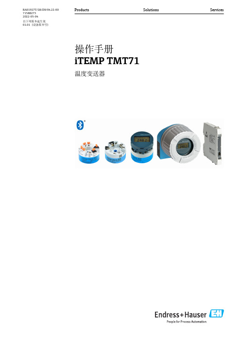
Products Solutions Services操作手册iTEMP TMT71温度变送器BA01927T/28/ZH/04.22-00715882732022-05-04自下列版本起生效01.01(设备版本号)iTEMP TMT71目录Endress+Hauser 3目录1文档信息 (4)1.1文档功能 (4)1.2《安全指南》(XA) (4)1.3信息图标 (4)1.4工具图标 (5)1.5文档资料 (6)1.6注册商标 (6)2基本安全指南 (7)2.1人员要求 (7)2.2预定用途 (7)2.3操作安全 (7)3到货验收和产品标识 (8)3.1到货验收 (8)3.2产品标识 (8)3.3制造商名称和地址 (9)3.4供货清单 (9)3.5证书和认证 (9)3.6储存和运输 (9)4安装 (11)4.1安装条件 (11)4.2安装 (11)4.3安装后检查 (16)5电气连接 (17)5.1接线要求 (17)5.2快速接线指南 (18)5.3连接传感器电缆 (19)5.4连接变送器 (19)5.5保证防护等级 (21)5.6连接后检查 (21)6操作方式 (22)6.1操作方式概述 (22)6.2操作菜单的结构和功能 (25)6.3通过调试软件访问操作菜单 (27)6.4通过SmartBlue App 访问操作菜单 (28)7系统集成 (30)7.1设备描述文件概述 (30)7.2测量变量 (30)8调试 (31)8.1安装后检查 (31)8.2启动变送器 (31)8.3设置测量设备 (31)8.4进行写保护设置,防止未经授权的访问 (33)9诊断和故障排除...................349.1常规故障排除........................349.2现场显示单元上的诊断信息..............369.3通过通信接口查看诊断信息..............369.4诊断信息列表........................369.5事件日志............................379.6诊断事件概览........................379.7固件变更历史........................3810维护..............................3911维修..............................3911.1概述...............................3911.2备件...............................3911.3返厂...............................3911.4处置...............................3912附件..............................3912.1设备专用附件........................4012.2通信专用附件........................4012.3服务专用附件........................4012.4系统产品............................4113技术参数..........................4213.1输入...............................4213.2输出...............................4313.3电源...............................4313.4性能参数............................4413.5环境条件............................5013.6机械结构............................5213.7证书和认证..........................5513.8文档资料............................5714操作菜单和菜单参数说明...........5814.1Diagnostics:诊断菜单.................6114.2Application:应用菜单.................6714.3System:系统菜单....................75索引.. (86)文档信息iTEMP TMT714Endress+Hauser1 文档信息1.1 文档功能《操作手册》包含设备生命周期内各个阶段所需的所有信息:从产品标识、到货验收和储存,至安装、电气连接、操作和调试,以及故障排除、维护和废弃。

ANPQP手册编辑整理:尊敬的读者朋友们:这里是精品文档编辑中心,本文档内容是由我和我的同事精心编辑整理后发布的,发布之前我们对文中内容进行仔细校对,但是难免会有疏漏的地方,但是任然希望(ANPQP手册)的内容能够给您的工作和学习带来便利。
同时也真诚的希望收到您的建议和反馈,这将是我们进步的源泉,前进的动力。
本文可编辑可修改,如果觉得对您有帮助请收藏以便随时查阅,最后祝您生活愉快业绩进步,以下为ANPQP手册的全部内容。
A.N。
P.Q。
P。
ANPQP 指南是为了将 Renault 和 Nissan 对全球供应商在新但是为了维持各公司的品牌特征,在某以 QS9000 APQP(产品品质先期策划和控制计划)为基础,5 个阶段。
ANPQP 阶段示意图显示了新车型开发时5 个阶段的联系,而且显示了主要的节点,这些节点表示进入每一新阶段所必须完成的工作。
Renault 和 Nissan 各自的节点显示在ANPQP的阶段与项目基本日程对照示意图中。
各项目特定的时程应与Renault 和/或 Nissan 的项目负责人一起在适当时间进行确认.某一项目的反馈结果将用作下一项目的第一阶段的输入。
高级管理层承诺对实现项目所有目的和目标给予充分支持,是贯穿 ANPQP 5个阶段的基本要求。
请注意, Renault 和/或 Nissan 保留在其认为适当时,随时对供应商进行现场审核的权利。
ANPQP 的目的为供应商开发新产品时可以达到Renault / Nissan联盟的品质、成本和交货期(QCD) 目标,指定所需采用的方法。
ANPQP 的适用范围ANPQP 是从项目初始策划阶段直至 SOP 和进入满负荷生产阶段,对供应商提出的联合要求。
请参阅ANPQP的持续性和其他 ASG 项目. ANPQP 应当在产品和/或工艺更改时应用,产品和/或工艺更改在产品的整个寿命周期都可能发生.ANPQP 适用于所有外部供应商,包括车辆、驱动系统、原材料和服务备件等,还适用于生产零件的内部供应商。

Document # SRAM111 REV BFEATURESFull CMOS, 6T CellHigh Speed (Equal Access and Cycle Times)– 10/12/15/20/25/35/45 ns (Commercial)– 12/15/20/25/35 /45 ns (Industrial)– 15/20/25/35/45/55/70/85 ns (Military)Low Power Operation – 743 mW Active -10– 660/770 mW Active for -12/15– 550/660 mW Active for -20/25 /35– 193/220 mW Standby (TTL Input)– 83/110 mW Standby (CMOS Input) P4C187– 5.5 mW Standby (CMOS Input) P4C 187L (Military)Single 5V±10% Power SupplyP4C187/P4C187LULTRA HIGH SPEED 64K x 1STATIC CMOS RAMSPIN CONFIGURATIONSFUNCTIONAL BLOCK DIAGRAM DIP (P3, D3, C3)LCC Pin configurations at end of datasheet.Data Retention with 2.0V Supply (P4C187L Military)Separate Data I/O Three-State Output TTL Compatible Output Fully TTL Compatible Inputs Standard Pinout (JEDEC Approved)– 22-Pin 300 mil DIP – 24-Pin 300 mil SOJ– 22-Pin 290x490 mil LCC – 28-Pin 350x550 mil LCCDESCRIPTIONThe P4C187/P4C187L are 65, 536-bit ultra high speed static RAMs organized as 64K x 1. The CMOS memories require no clocks or refreshing and have equal access and cycle times. The RAMs operate from a single 5V ± 10%tolerance power supply. Data integrity is maintained for sup-ply voltages down to 2.0V, typically drawing 10µA.Access times as fast as 10 nanoseconds are available,greatly enhancing system speeds. CMOS reduces powerconsumption to a low 743mW active, 193/83mW standby for TTL/CMOS inputs and only 5.5 mW standby for the P4C187L.The P4C187/P4C187L are available in 22-pin 300 mil DIP,24-pin 300 mil SOJ, 22-pin and 28-pin LCC packages pro-viding excellent board level densities.P4C187/187LMAXIMUM RATINGS (1)Symbol Parameter Value Unit V CCPower Supply Pin with –0.5 to +7VRespect to GND Terminal Voltage with –0.5 to V TERM Respect to GND V CC +0.5V (up to 7.0V)T AOperating Temperature–55 to +125°CSymbol Parameter Value Unit T BIAS Temperature Under –55 to +125°C BiasT STG Storage Temperature –65 to +150°C P T Power Dissipation 1.0W I OUTDC Output Current50mARECOMMENDED OPERATINGTEMPERATURE AND SUPPLY VOLTAGEI SBStandby Power Supply Current (TTL Input Levels)CE ≥ V IH Mil.V CC = Max ., Ind./Com’l.f = Max., Outputs Open ______4035____________201540n/a 1.0n/amAmA______CE ≥ V HC Mil.V CC = Max., Ind./Com’l.f = 0, Outputs Open V IN ≤ V LC or V IN ≥ V HCStandby Power Supply Current(CMOS Input Levels)I SB1Grade(2)Ambient TemperatureGND V CC0V 0V5.0V ± 10%5.0V ± 10%0V 5.0V ± 10%–55°C to +125°C Symbol C IN C OUTParameter Input Capacitance Output CapacitanceConditions V IN = 0V V OUT = 0V57Unit pF pFCAPACITANCES (4)V CC = 5.0V, T A = 25°C, f = 1.0MHz n/a = Not ApplicableSymbol DC ELECTRICAL CHARACTERISTICSOver recommended operating temperature and supply voltage (2)V IH V IL V HC V LC V CD V OL V OH I LI I LO ParameterInput High Voltage Input Low Voltage CMOS Input High Voltage CMOS Input Low VoltageInput Clamp Diode Voltage Output Low Voltage (TTL Load)Output High Voltage (TTL Load)Input Leakage Current Output Leakage CurrentTest ConditionsV CC = Min., I IN = 18 mA I OL = +8 mA, V CC = Min.I OH = –4 mA, V CC = Min.V CC = Max. Mil.V IN = GND to V CC Com’l.V CC = Max., CE = V IH , Mil.V OUT = GND to V CC Com’l.P4C187Min 2.2–0.5(3)V CC –0.2–0.5(3)2.4–10–5–10–5Max V CC +0.50.8V CC +0.50.2–1.20.4+10+5+10+5P4C187LMin Max 2.2–0.5(3)V CC –0.2–0.5(3)2.4–5n/a –5n/a V CC +0.50.8V CC +0.50.20.4–1.2+5n/a +5n/a UnitV V V V V V V µA µA Notes:1.Stresses greater than those listed under MAXIMUM RATINGS may cause permanent damage to the device. This is a stress rating only and functional operation of the device at these or any other conditions above those indicated in the operational sections of this specification is not implied. Exposure to MAXIMUM rating conditions for extended periods may affect reliability.2.Extended temperature operation guaranteed with 400 linear feet per minute of air flow.3.Transient inputs with V IL and I IL not more negative than –3.0V and –100mA, respectively, are permissible for pulse widths up to 20 ns.4.This parameter is sampled and not 100% tested.itaryIndustrial–40°C to +85°C 0°C to +70°C Commercial*V CC = 5.5V. Tested with outputs open. f = Max. Switching inputs are 0V and 3V. CE = V IL .DATA RETENTION CHARACTERISTICS (P4C187L Military Temperature Only)Symbol V DR I CCDR t CDR t R †ParameterV CC for Data Retention Data Retention Current Chip Deselect to Data Retention Time Operation Recovery TimeTest Conditons CE ≥ V CC –0.2V,V IN ≥ V CC –0.2V or V IN ≤ 0.2VMin 2.00t RC §Typ.*V CC = 2.0V 3.0V Max V CC = 2.0V 3.0VUnit 1015600900VµA ns ns*T A = +25°C§t RC = Read Cycle Time†This parameter is guaranteed but not tested.DATA RETENTION WAVEFORMI CCSymbol ParameterTemperature RangeDynamic Operating Current*Commercial Industrial Military–10N/A–12–15–20–25–35–45Unit N/A mA mA mAPOWER DISSIPATION CHARACTERISTICS VS. SPEEDN/A 150155160170180N/A170160155150145180170160155150N/A N/A –85N/A 145N/A –70N/A 145N/A –55N/A 145N/AP4C187/187LNotes:5.CE is LOW and WE is HIGH for READ cycle.6.WE is HIGH, and address must be valid prior to or coincident with CE transition LOW.7.Transition is measured ±200mV from steady state voltage prior to change with specified loading in Figure 1. This parameter is sampled and not 100% tested.8.Read Cycle Time is measured from the last valid address to the first transitioning address.TIMING WAVEFORM OF READ CYCLE NO. 2(6)TIMING WAVEFORM OF READ CYCLE NO. 1(5)AC CHARACTERISTICS—READ CYCLE(V CC = 5V ± 10%, All Temperature Ranges)(2)Notes:9.CE and WE must be LOW for WRITE cycle.10.If CE goes HIGH simultaneously with WE HIGH, the output remainsin a high impedance state.11.Write Cycle Time is measured from the last valid address to the firsttransition address.TIMING WAVEFORM OF WRITE CYCLE NO. 1 (WE CONTROLLED)(9)AC CHARACTERISTICS - WRITE CYCLE(V CC = 5V ± 10%, All Temperature Ranges)(2)P4C187/187LTIMING WAVEFORM OF WRITE CYCLE NO. 2 (CE CONTROLLED)(9)Figure 1. Output LoadFigure 2. Thevenin Equivalent* including scope and test fixture.Note:Due to the ultra-high speed of the P4C187/L, care must be taken when testing this device; an inadequate setup can cause a normal functioning part to be rejected as faulty. Long high-inductance leads that cause supply bounce must be avoided by bringing the V CC and ground planes directly up to the contactor fingers. A 0.01 µF high frequency capacitor is also required between V CCand ground. To avoid signal reflections,proper termination must be used; for example, a 50Ω test environment should be terminated into a 50Ω load with 1.73V (Thevenin Voltage) at the comparator input, and a 116Ω resistor must be used in series with D OUT to match 166Ω (Thevenin Resistance).AC TEST CONDITIONSTRUTH TABLEInput Pulse Levels GND to 3.0VInput Rise and Fall Times 3ns Input Timing Reference Level 1.5V Output Timing Reference Level 1.5VOutput LoadSee Figures 1 and 2Mode CE WE Output Power Standby H X High Z Standby Read L H D OUT Active WriteLLHigh ZActiveP4C187/187LORDERING INFORMATIONSELECTION GUIDEThe P4C187 is available in the following temperature, speed and package options. The P4C187L is only available over the military temperature range.* Military temperature range with MIL-STD-883, Class B processing.N/A = Not AvailableCERDIP DUAL IN-LINE PACKAGEP4C187/187LSOJ SMALL OUTLINE IC PACKAGERECTANGULAR LEADLESS CHIP CARRIER PLASTIC DUAL IN-LINE PACKAGEP4C187/187LREVISIONSDOCUMENT NUMBER:SRAM111DOCUMENT TITLE:P4C187 / P4C187L ULTRA HIGH SPEED 64K x 1 STATIC CMOS RAMSREV.ISSUEDATEORIG. OFCHANGEDESCRIPTION OF CHANGEOR1997DAB New Data SheetA Oct-05JDB Change logo to PyramidB Apr-07JDB Added 55, 70, and 85 ns speeds 元器件交易网。

Data SheetCisco ATA 187 Analog Telephone AdaptorProduct OverviewThe Cisco® ATA 187 Analog Telephone Adaptor is a handset-to-Ethernet adaptor that turns traditional telephone devices into IP devices. Customers can take advantage of the many new and exciting IP telephony applications by connecting their analog devices to Cisco ATAs.The Cisco ATA products are standards-based communication devices that deliver true, next-generation voice-over-IP (VoIP) terminations to businesses and residences worldwide.●Protects existing telephone investment: The Cisco ATA 187 supports two voice ports, each with its ownindependent telephone number, and a single RJ-45 10/100 BASE-T Ethernet port. This adaptor can make use of existing Ethernet LANs in addition to broadband pipes such as DSL, fixed wireless, and cable modem deployments.●Cost effective: The Cisco ATA 187 helps customers turn their analog phone devices into IP devices costeffectively and is the preferred solution to address the needs of customers who connect to enterprisenetworks, small-office environments, or the emerging VoIP managed voice services and local servicesmarket.Enterprise customers are using the Cisco ATA 187 to connect analog phones and fax machines to their VoIP network. Service providers are taking advantage of emerging telephony applications and the ease of deploying second-line services using the Cisco ATA 187 (Figures 1 and 2).Figure 1. Cisco ATA 187: Endpoint for an End-to-End Broadband SystemFigure 2. Cisco ATA 187 as Endpoint in Session Initiation Protocol (SIP) Network* DSL and cable mode need SIP support.Features and BenefitsTable 1 lists the features and benefits of the Cisco ATA 187.Table 1.Features and BenefitsFeatureBenefits Configuration and Provisioning● Configuration as per Cisco endpoints devices● Autoprovisioning with Trivial File Transfer Protocol (TFTP) for servers ● Automatic assignment of IP address, network routing IP, and subnet mask using Dynamic Host Configuration Protocol (DHCP) ● Touch-tone telephone keypad configuration with voice prompt ● Administration password to protect configuration and access ● Remote upgrades through network● Cisco Unified Communications Manager (UCM) standard configuration and provisioning options ● Ease of administrationVoice Quality● Advanced preprocessing to optimize full-duplex voice compression ● High-performance line-echo cancellation to eliminate noise and echo ● Voice activity detection (VAD) and comfort noise generation (CNG) to save bandwidth by delivering voice, not silence● Dynamic network monitoring to reduce jitter artifacts such a packet lossClear, natural-sounding voice qualitySignaling Protocol● Session Initiation Protocol (SIP) on the Cisco line sideAllows interoperation with Cisco UCM SIP solution Security● Secure Real-Time Transfer Protocol and Transport Layer Security (SRTP/TLS) over SIPSecure media and secure signaling support, for secure solutions Fax Support● T38 fax supportStandard fax capability to send faxes over the IP network Form Factor● Fits in most environmentsNew form-factor design based on the Cisco endpoints portfolio Cisco UCM Version Compatibility●Cisco UCM Versions 7.1.5, 8.0.2, or higherProduct SpecificationsTable 2 presents the specifications for the Cisco ATA 187.Table 2. Product SpecificationsPhysical SpecificationsPower Power supply: Universal AC power supply 100 and 240VPower adaptor output voltage: +12.0 VDC at 1A maximum Noise level Less than 34 dBA at 3 feetConnectors 2 RJ 11Thermal Operating temperature: 23 to 113°F (5 to 45 °C)Non-operating temperature: -13 to 158ºF (-25 to 70ºC) Humidity Operating humidity: 5 to 95% noncondensingMean time between failure (MTBF) 100,000 hoursPhysical dimensions (H x W x D) and weight Dimensions: 1.5 x 5.4 x 6.7 in. (3.8 x 13.7 x 17.0 cm) Weight: 9.2 oz (260g)Compliance RoHS- and WEEE-compliant materialsOn-off switch To turn device on and offSoftware SpecificationsCisco ATA SIP services ●IP address assignment: Provided by DHCP or statically configured●Cisco ATA configuration through Cisco UCM configuration interface●VLAN configuration●Cisco Discovery Protocol●Low-bit-rate codec selection●User authentication●Configurable tones (dial tone, busy tone, alert tone, reorder tone, and call-waiting tone)●Dial plans●SIP proxy server redundancy●Privacy features●Domain Name System (DNS) service (SRV) support●User-configurable, call waiting; permanent default setting●Comfort noise during silence period when using G.711●Advanced audio mode●Caller ID format●Ring cadence format●Silence suppression●Hook-flash detection timing configuration●Configurable on-hook delay●Type of service (ToS) configuration for audio and signaling Ethernet packets●Debugging and diagnostic toolsSIP services Cisco ATA supports the methods listed here (for more information, refer to RFC-3261):●REGISTER●REFER●INVITE●BYE●CANCEL●NOTIFY●OPTIONS●ACK●SUBSCRIBESupplementary services ●Caller ID●Call-waiting caller ID●Voice-mail indication●Conference call●Call waiting●Call forwarding●Calling-line identification●Unattended transfer●Attended transfer●Shared line●Speed dial●Meet me●Pick up●RedialOther supported protocols ●IEEE 802.1Q VLAN tagging●Cisco Discovery Protocol●DNS●DHCP●Internet Control Message Protocol (ICMP)●IP●Real-Time Transport Protocol (RTP)●TCP●Trivial File Transfer Protocol (TFTP)●User Datagram Protocol (UDP)Fax services The Cisco ATA supports two modes of fax services, in which fax signals are transmitted using the G.711codec:●Fax pass-through mode: The mode enables receiver-side called-station-identification (CED) tonedetection with automatic G.711A-law or G.711µ-law switching.●T38 fax relay mode: The T.38 fax relay feature enables devices to use fax machines to send files over theIP network. In general, when a fax is received, it is converted to an image, sent to the T.38 fax device,and converted back to an analog fax signal. T.38 fax relays configured with voice gateways decode ordemodulate the fax signals before they are transported over IP.Note: Success of fax transmission depends on network conditions and the fax modem response to theseconditions. The network must have reasonably low network jitter, network delay, and packet loss rate.Voice codecs supported ●G.711µ-law●G.711A-law●G.729●G.729A●G.729B●G.729ABSRTP/TLS ●SRTP secures voice conversations on the network and provides protection against replay attacks.●TLS is a cryptographic protocol that secures data communications such as email on the Internet. TLS isfunctionally equivalent to SSL.VoIP specifications ●LAN port: One RJ-45 10/100BASE-T Fast Ethernet port●Quality of service (QoS): Precedence setting and differentiated services code point (DSCP)Call progress tones Configurable based on network localeLine-echo cancellation ●Echo canceller for each port●8-millisecond (ms) echo length●Nonlinear echo suppression (echo return loss [ERL] greater than 28 dB for f = 300 to 3400 Hz)System RequirementsFigure 3 shows the system setup.Figure 3. System SetupWarranty InformationFind warranty information on at the Product Warranties page.Ordering InformationHelp customers understand all the components or parts they need to purchase to install and use the product. This section also provides a direct link to the Cisco Ordering Tool, and Table 3 lists part numbers for customer convenience.To place an order, visit the Cisco Ordering homepage. To download software, visit the Cisco Software Center. Table 3. Ordering InformationProduct Name Part NumberCisco ATA 187 ATA187-I1-A=Product Name Part NumberATA power supply cables for Taiwan ATA187PWRCORD-TWNATA power supply cables for Brazil ATA187PWRCORD-UCATA power supply cables for North America ATA187PWRCORD-NAATA power supply cables for Japan ATA187PWRCORD-JPProduct Name Part NumberATA power supply cables for Continent Europe ATA187PWRCORD-EUATA power supply cables for United Kingdom ATA187PWRCORD-UKATA power supply cables for Australia ATA187PWRCORD-AUATA power supply cables for China ATA187PWRCORD-CCCATA power supply cables for Argentina ATA187PWRCORD-IRAMATA power supply cables for India ATA187PWRCORD-INDATA power supply cables for Mexico ATA187PWRCORD-MEXATA power supply cables for Saudi Arabia ATA187PWRCORD-SAUDATA power supply cable for South Africa ATA187PWRCORD-SABCisco ServicesCisco Services integrates closely with consumer marketing teams as an essential element of any technology solution. Please contact your Cisco Services marketing communications manager if you have not already received targeted services content blocks for integration. Please email ******************* if you are not sure of the appropriate contact.Cisco Services make networks, applications, and the people who use them work better together.Today, the network is a strategic platform in a world that demands better integration between people, information, and ideas. The network works better when services, together with products, create solutions aligned with business needs and opportunities.The unique Cisco Lifecycle approach to services defines the requisite activities at each phase of the network lifecycle to help ensure service excellence. With a collaborative delivery methodology that joins the forces of Cisco, our skilled network of partners, and our customers, we achieve the best results.For More InformationUse this section to a “call to action” message. Insert your product-specific content in the standard wording below. If there is no alias, delete the “or” and the alias blank, and add a period after “representative.” Local account representative” should be linked to an appropriate general rep page, if available. Consider directing data sheet readers to white papers, solution overviews, case studies, or other marketing materials.For more information about the Cisco Enter Product Name, visit Enter URL for Product Home Page or contact your local account representative or Enter Cisco alias.。

DKWF121 – WF121-A 802.11 B/G/N MODULE EVALUATION BOARDPRELIMINARY DATA SHEETWednesday, 16 May 2012Version 0.5Copyright © 2000-2012 Bluegiga TechnologiesAll rights reserved.Bluegiga Technologies assumes no responsibility for any errors which may appear in this manual. Furthermore, Bluegiga Technologies reserves the right to alter the hardware, software, and/or specifications detailed here at any time without notice and does not make any commitment to update the information contained here. Bluegiga’s products are not authorized for use as critical c omponents in life support devices or systems.The WRAP, Bluegiga Access Server, Access Point and iWRAP are registered trademarks of Bluegiga Technologies.The Bluetooth trademark is owned by the Bluetooth SIG Inc., USA and is licensed to Bluegiga Technologies. All other trademarks listed herein are owned by their respective owners.VERSION HISTORYTABLE OF CONTENTS1Product description (5)2Ordering Information (6)3Board Description (7)3.1WiFi Module (7)3.2Crystals (7)3.3Configurable I/O Ports (7)3.4Bluetooth Coexistence (8)3.5LEDs and Buttons (8)3.6USB Connections (9)3.7Board Power (10)3.8Current Measurement Point J13 (10)3.9VDD_PA Selection Header J7 (10)3.10Ethernet (11)3.11Programming Connections (11)3.12Debug SPI Interface (12)3.13Prototyping Area (12)4Board layout (13)5Contact Information (14)1 Product descriptionDESCRIPTIONDKWF121 is intended for evaluating the WF121 Wi-Fi module and as a basis for product development. The board contains connectors for easy development with a PC using the main host connections, USB and UART through a USB converter. Also present are headers for all the GPIO pads connected around a prototyping area for easy connection of pin headers with custom pinouts, sensors etc.The WF121 is a self-contained Wi-Fi module providing a fully integrated 2.4GHz 802.11 b/g/n radio and a 32-bit microcontroller (MCU) platform, making it an ideal product for embedded applications requiring simple, low-cost and low-power wireless TCP/IP connectivity. WF121 also provides flexible interfaces for connecting to various peripherals. WF121 allows end user applications to be embedded onto the on-board 32-bit microcontroller using a simple Bluegiga BGScript TM scripting language. This cuts out the need of an external MCU and allows the development of smaller and lower-cost products. However WF121 can also be used in modem-like mode in applications where the external MCU is needed.With an integrated 802.11 radio, antenna, single power supply, and regulatory certifications, WF121 provides a low-risk and fast time-to-market for applications requiring Wi-Fi connectivity. This co mbined with Bluegiga’s excellent customer service will turn your Internet-of-Things applications into reality. KEY FEATURES:-USB or UART host connection-USB converter for the UART-Can be powered through USB-Current measurement voltage output -Prototyping areaPHYSICAL OUTLOOK:2 Ordering InformationConfidentialConfidential 3Board Description3.1 WiFi ModuleDKWF121 contains a WF121-A module variant, with an internal chip antenna.3.2 CrystalsThere are two crystals assembled on DKWF121, an 8MHz crystal for the WF121 CPU clocking and a32.768kHz crystal for the CPU real time clock. The 8MHz crystal is needed when the WF121 USB connection is used, otherwise it is not essential. The 32kHz crystal is also optional, and if extra GPIO are needed, the 0ohm resistors connecting the crystals to the module can be removed and moved to connect the pin headers and prototyping area pads to the module pads. The pads are not connected to the pin headers by default as crystal connections are always sensitive to noise.3.3Configurable I/O PortsAll the GPIO pads available on the WF121 are routed to pin headers for easy connection to other boards or a logic analyzer. All the signals are also available on through-hole pads on the edges of the board prototyping area for easy development prototyping.The GPIO signals associated with the crystals are routed but not connected due to the presence of the crystals, but if required the crystals can be removed and the associated 0ohm resistors moved to connect the signals to the headers.The signals shared for other functions like the ICSP programming interfac e, JTAG, UART’s and Ethernet should not be driven by externally connected outputs when the mentioned functions are used to avoid damage. The UART and Ethernet signals are disconnected when the associated on-board chips are disabled with the on-board switches.The USB pins are by default disconnected from the pin headers, but can be connected by adding two jumpers to the specific header.3.4 Bluetooth CoexistenceIndustry standard 2-wire and 3-wire, as well as Unity-3, Unity-4, Unity-3e coexistence schemes are supported as well as the Unity+ -extension, and the associated signals are available. The PIO pads can be configured for these functions among others. A U.FL connector is also present for antenna sharing using the module internal RF switch. As only 4 GPIO signals can be used for coexistence, antenna sharing in practice requires the use of the CSR proprietary Unity-3e or 3e+ scheme.3.5 LEDs and ButtonsThere are five LEDs and five pushbuttons on the DKWF121. One button is for module reset and one LED indicates that the module has a power supply present, while the other four LEDs and buttons are available for development purposes. The LEDs are buffered with MOSFETs and the buttons are open when unpressed, allowing the connected GPIO lines to be used for other purposes without disconnecting the LEDs or buttons.Confidential3.6USB Connectionsoperating systems with either inbuilt or automatically installed drivers.ConfidentialConfidential No separate connectors for SPI host connections are provided as there is no standard connector or pinout, but the signals are available on the pin headers and pads on the prototyping area edge for easy soldering of a connector with a custom pinout.3.7Board PowerDKWF121 can be powered by several sources.∙ Both USB connectors can be used as the power supply input ∙ A two-pin header∙The signal pin headers and prototyping area connections have power connectionsNote: if the on-board WF121 module does not contain firmware that operates the native USB connection, the module cannot request an increase to the USB default current limit of 100mA. Although not all USB host systems implement it, the USB specification states that the host should limit the current output to 100mA unless an increase is requested, and using the module with high transmit duty cycles may cause the USB host to go into current limit, possibly causing the module to crash. It is preferred to power the board through the USB/UART-converter connector, the converter chip will automatically request for an increased current limit. The board contains a switch mode converter that converts the 5V input to the 3.3V supply required by the module. The converter is specified for output currents up to 600mA, allowing up to 200mA to be drawn for powering customer applications.The module operates down to 2.7V, but the current measure output and USB host functionality require a regulated 5V input. The header and the USB connectors also have series schottky diodes, increasing the minimum input voltage slightly. The 5V power connections in the prototyping area and the associated pin headers do not have series diodes. The diodes allow connection of a USB host together with a separate power supply without risk of damage.3.8 Current Measurement Point J13Header J13 contains a jumper that connects the switch mode regulator to the module 3.3V supply pads. The jumper can be removed and the average current consumption of the module can be measured with a multimeter or a series resistor can be inserted for measuring the momentary current consumption of the module with an oscilloscope. Note that for average consumption measurement of anything else besides sleep current a fast RMS multimeter is needed due to the pulsed nature of the consumption.Removing the jumper also allows separation of the module supply lines from the regulator output, for example when using an external regulator to supply the 3.3V voltage to the module is desired.3.9 VDD_PA Selection Header J7WF121 has two power supply inputs, VDD_3.3V (VDD_3.3V_MOD line on the schematic) and VDD_PA. The VDD_3.3V pad supplies the internal processor and has a voltage range of 2.3V to 3.6V. The VDD_PA pad supplies the internal WiFi-circuitry through a switch mode converter and the WiFi power amplifier directly. TheVDD_PA line can operate with input voltages between 2.7V and 5.5V, though the power consumption of the power amplifier will grow in direct proportion to the input voltage. The separate supply however allows direct connection to a lithium-ion battery, with just a small linear regulator limiting the supply voltage for the processor side.A jumper at header J7 usually connects VDD_PA to the board 3.3V switch mode converter output. The jumper can be moved to the alternate position to supply the VDD_PA line directly from the 5V supply rail, for example for connecting directly to a lithium battery either through the power input header or through the prototyping area connections.3.10EthernetThe board contains a 10/100Mbps Ethernet PHY with all the associated components, connected to the module internal Ethernet MAC with an RMII interface. The PHY can be fully powered off and disconnected from the GPIO lines using switch SW1, allowing the GPIO lines to be used for other functions. The Ethernet interface is not yet supported by the Bluegiga software.3.11Programming ConnectionsDKWF121 contains two connectors that allow direct programming of the WF121 internal processor. The Microchip proprietary ICSP bus allows programming the full firmware image using a Microchip or third party programming adapter. The pin header installed on the DKWF121 has a pinout suitable for use with the low-Confidentialcost PicKit3 programming tool from Microchip. A JTAG connection is also available for basic boundary scans and device programming. The JTAG does not support full device testing and debugging.The primary means of uploading application data is through a host connection through the Bluegiga boot loader. The programming connections should not be needed unless the internal boot loader is overwritten by the application.3.12 Debug SPI InterfaceA header is provided for the module debug bus for certification RF testing. Access to internal settings and test modes is available using a CSR compatible SPI adapter and UniTest-software.For more information contact Bluegiga technical support.3.13 Prototyping AreaDKWF121 contains an array of through plated holes with wide pads with a 2.54mm raster for easy addition of carrier boards, through-hole components and pin headers with a custom pinout. Also present is a smaller array of pads with no holes using 1.27m raster for connecting SMD components like sensors, regulators etc during system development.All GPIO signals are routed to the prototyping area edges, though some of them are not by default connected due to function multiplexing. See other chapters for detailed descriptions of these signals.Also present on the pin headers and pads around the prototyping area are several supply voltage rails present on the board. These can be used for powering external circuitry, or for powering the module with external power sources. The uppermost and lowest rows of pads are connected to ground.Confidential4 Board layoutConfidential5 Contact InformationSales:******************Technical support:********************Orders: *******************WWW: www.bluegiga.hkHead Office / Finland:Phone: +358-9-4355 060Fax: +358-9-4355 0660Sinikalliontie 5A02630 ESPOOFINLANDPostal address / Finland:P.O. BOX 12002631 ESPOOFINLANDSales Office / USA:Phone: +1 770 291 2181Fax:+1 770 291 2183Bluegiga Technologies, Inc.3235 Satellite Boulevard, Building 400, Suite 300Duluth, GA, 30096, USASales Office / Hong-Kong:Phone: +852 3182 7321Fax:+852 3972 5777Bluegiga Technologies, Inc.19/F Silver Fortune Plaza, 1 Wellington Street,Central Hong KongConfidential。

LIS8712 7W 35V-46V/150mA全电压应用LED驱动方案Typ input:100Vac/60Hz~240Vac/50Hz; Output:35V~46V/150mA以下方案参数,仅为典型应用,用户需根据终端的实际使用环境进行验证一:原理图二:物料表No. Position Description Quantity1 R1,R2 SMD RES 1206 150K ±5% 22 R3 Floating(NC)03 R4 SMD RES 1206 2R7 ±1% (output current:150mA) 14 R6 SMD RES 0805 47K ±5% 15 C1 E.C 6.8uF/400V 105℃Ø8*16mm 16 C2 E.C 1uF/50V 105℃Ø5*11mm 17 C3 E.C 47uF/100V 105℃Ø8*12mm 18 BD1 BR-MBS-0.5A-600V-MB6F 19 D1 DIO-FAS-SMA-1.00A-400V-ES1G 110 T1 EE13 5+5PIN 立式1.9mH 111 PCB PCB-FR4-18.5mm*38mm*1.2mm 112 IC LIS8712 SOP-7 113 CY1 Y1电容222M/250-400Vac P=7.5mm 1 三:变压器资料1)骨架:EE-13(5+5Pin立式)2)磁芯材质:PC40(TDK)3)原边电感量(pin1‐5):1.90mH ±5% (50KHz, 1V, 25℃)步骤 层数 脚位 线径 匝数 绕线方式1 P1 Pin5→2 Φ0.15mm漆包线 80Ts,2层平整密绕 顺时针2 Tape ‐ 2Ts3 S1 Pin10→6 Φ0.23mm漆包线 83Ts,3层平整密绕 顺时针4 Tape ‐ 2Ts5 P2 Pin2→1 Φ0.15mm漆包线 70Ts,2层平整密绕顺时针 1:说明1)2:注意事项1)pin3需拔掉;2)所有绕线均为铜线,绕线时应均匀绕制,且绕满一层;3)所有产品应真空含浸,要求全检,确保品质。

VOLTAGE RANGE 20 to 40 Volts CURRENT 1.0 AmpereMAXIMUM RATINGS (@ T A =25 C unless otherwise noted)ELECTRICAL CHARACTERISTICS (@T A =25 C unless otherwise noted)RATINGSMaximum Recurrent Peak Reverse Voltage Maximum RMS Voltage Maximum DC Blocking VoltageMaximum Average Forward Rectified Current .375” (9.5mm) lead length at T L =90CPeak Forward Surge Current 8.3 ms single half sine-wave superimposed on rated load (JEDEC method)T Typical Thermal Resistance (Note 3)ypical Junction Capacitance (Note 1)SYMBOL V RRM V DC I FSM C J T STGV RMS UNITS Volts Volts Volts Amps 1.025*******Amps0C Storage Temperature RangeI R q JA R q JL O 150pFOperating Temperature Range T J 1N58171N58181N58191N58171N58181N5819203040142128203040-55 to + 150CC/W NOTES : 1. Me 3. Thermal Resistance : At 9.5mm lead lengths, PCB mounted.asured at 1 MHz and applied reverse voltage of 4.0 volts.2006-12CHARACTERISTICSMaximum Average Reverse Current at Rated DC Blocking VoltageV F SYMBOL I RmAmps Maximum Instantaneous Forward Voltage at 1.0A DC Volts 0.210@T A = 25oC @T A = 100o C.45.55.60V F Maximum Instantaneous Forward Voltage at 3.1A DC Volts .750.8750.90mAmps UNITS 2. “Fully ROHS compliant”, “100% Sn plating (Pb-free)”.DO-41INSTANTANEOUS FORWARD VOLTAGE, (V)PERCENT RATED PEAK REVERSE VOLTAGE, (%)I N S T A N T A N E O U S F O R W A R D C U R R E N T , (A )LEAD TEMPERATURE, (C)0.10.11.01020A V E R A G E F O R W A R D C U R R E N T , (A )C T , T O T A L C A P A C I T A N C E , (p F )1.7 1.91.30.50.30.90.7 1.1 1.52.11751501251007550250.0010.10.011.010100RATING AND CHARACTERISTICS CURVES ( 1N5817 THRU 1N5819 )FIG.3 TYPICAL REVERSE CHARACTERISTICSFIG.1 TYPICAL FORWARD CURRENT DERATING CURVEFIG.2 TYPICAL INSTANTANEOUS FORWARD CHARACTERISTICSREVERSE VOLTAGE, (V)I N S T A N T A N E O U S R E V E R S E C U R R E N T , (m A )1010080604020200400FIG.4 TYPICAL JUNCTION CAPACITANCENUMBER OF CYCLES AT 60HzP E A K F O R W A R D S U R G E C U R R E N T , (A )105152520FIG.5 MAXIMUM NON-REPETITIVE FORWARD SURGE CURRENTRectron Inc reserves the right to make changes without notice to any productspecification herein, to make corrections, modifications, enhancements or other changes. Rectron Inc or anyone on its behalf assumes no responsibility or liabi- lity for any errors or inaccuracies. Data sheet specifications and its information contained are intended to provide a product description only. "Typical" paramet- ers which may be included on RECTRON data sheets and/ or specifications ca- n and do vary in different applications and actual performance may vary over ti- me. Rectron Inc does not assume any liability arising out of the application or use of any product or circuit.Rectron products are not designed, intended or authorized for use in medical, life-saving implant or other applications intended for life-sustaining or other rela- ted applications where a failure or malfunction of component or circuitry may di- rectly or indirectly cause injury or threaten a life without expressed written appr- oval of Rectron Inc. Customers using or selling Rectron components for use in such applications do so at their own risk and shall agree to fully indemnify Rect- ron Inc and its subsidiaries harmless against all claims, damages and expendit- ures.DISCLAIMER NOTICE。