KK74ACT20中文资料
- 格式:pdf
- 大小:163.69 KB
- 文档页数:5

PACKAGING INFORMATIONOrderable Device Status (1)Package Type Package Drawing Pins Package Qty Eco Plan (2)Lead/Ball FinishMSL Peak Temp (3)74ACT11174DW OBSOLETE SOIC DW 20TBD Call TI Call TI 74ACT11174DWR OBSOLETE SOIC DW 20TBD Call TI Call TI 74ACT11174DWR OBSOLETE SOIC DW 20TBD Call TI Call TI 74ACT11174N OBSOLETE PDIP N 20TBD Call TI Call TI 74ACT11174NOBSOLETEPDIPN20TBDCall TICall TI(1)The marketing status values are defined as follows:ACTIVE:Product device recommended for new designs.LIFEBUY:TI has announced that the device will be discontinued,and a lifetime-buy period is in effect.NRND:Not recommended for new designs.Device is in production to support existing customers,but TI does not recommend using this part in a new design.PREVIEW:Device has been announced but is not in production.Samples may or may not be available.OBSOLETE:TI has discontinued the production of the device.(2)Eco Plan -The planned eco-friendly classification:Pb-Free (RoHS)or Green (RoHS &no Sb/Br)-please check /productcontent for the latest availability information and additional product content details.TBD:The Pb-Free/Green conversion plan has not been defined.Pb-Free (RoHS):TI's terms "Lead-Free"or "Pb-Free"mean semiconductor products that are compatible with the current RoHS requirements for all 6substances,including the requirement that lead not exceed 0.1%by weight in homogeneous materials.Where designed to be soldered at high temperatures,TI Pb-Free products are suitable for use in specified lead-free processes.Green (RoHS &no Sb/Br):TI defines "Green"to mean Pb-Free (RoHS compatible),and free of Bromine (Br)and Antimony (Sb)based flame retardants (Br or Sb do not exceed 0.1%by weight in homogeneous material)(3)MSL,Peak Temp.--The Moisture Sensitivity Level rating according to the JEDEC industry standard classifications,and peak solder temperature.Important Information and Disclaimer:The information provided on this page represents TI's knowledge and belief as of the date that it is provided.TI basesits knowledge and belief on information provided by third parties,and makes no representation or warranty as to the accuracy of such information.Efforts are underway to better integrate information from third parties.TI has taken and continues to take reasonable steps to provide representative and accurate information but may not have conducted destructive testing or chemical analysis on incoming materials and chemicals.TI and TI suppliers consider certain information to be proprietary,and thus CAS numbers and other limited information may not be available for release.In no event shall TI's liability arising out of such information exceed the total purchase price of the TI part(s)at issue in this document sold by TI to Customer on an annual basis.PACKAGE OPTION ADDENDUM24-Jun-2005Addendum-Page 1IMPORTANT NOTICETexas Instruments Incorporated and its subsidiaries(TI)reserve the right to make corrections,modifications,enhancements,improvements, and other changes to its products and services at any time and to discontinue any product or service without notice.Customers should obtain the latest relevant information before placing orders and should verify that such information is current and complete.All products are sold subject to TI’s terms and conditions of sale supplied at the time of order acknowledgment.TI warrants performance of its hardware products to the specifications applicable at the time of sale in accordance with TI’s standard warranty.Testing and other quality control techniques are used to the extent TI deems necessary to support this warranty.Except where mandated by government requirements,testing of all parameters of each product is not necessarily performed.TI assumes no liability for applications assistance or customer product design.Customers are responsible for their products and applications using TI components.To minimize the risks associated with customer products and applications,customers should provide adequate design and operating safeguards.TI does not warrant or represent that any license,either express or implied,is granted under any TI patent right,copyright,mask work right, or other TI intellectual property right relating to any combination,machine,or process in which TI products or services are rmation published by TI regarding third-party products or services does not constitute a license from TI to use such products or services or a warranty or endorsement e of such information may require a license from a third party under the patents or other intellectual property of the third party,or a license from TI under the patents or other intellectual property of TI.Reproduction of TI information in TI data books or data sheets is permissible only if reproduction is without alteration and is accompanied by all associated warranties,conditions,limitations,and notices.Reproduction of this information with alteration is an unfair and deceptive business practice.TI is not responsible or liable for such altered rmation of third parties may be subject to additional restrictions.Resale of TI products or services with statements different from or beyond the parameters stated by TI for that product or service voids all express and any implied warranties for the associated TI product or service and is an unfair and deceptive business practice.TI is not responsible or liable for any such statements.TI products are not authorized for use in safety-critical applications(such as life support)where a failure of the TI product would reasonably be expected to cause severe personal injury or death,unless officers of the parties have executed an agreement specifically governing such use.Buyers represent that they have all necessary expertise in the safety and regulatory ramifications of their applications,and acknowledge and agree that they are solely responsible for all legal,regulatory and safety-related requirements concerning their products and any use of TI products in such safety-critical applications,notwithstanding any applications-related information or support that may be provided by TI.Further,Buyers must fully indemnify TI and its representatives against any damages arising out of the use of TI products in such safety-critical applications.TI products are neither designed nor intended for use in military/aerospace applications or environments unless the TI products are specifically designated by TI as military-grade or"enhanced plastic."Only products designated by TI as military-grade meet military specifications.Buyers acknowledge and agree that any such use of TI products which TI has not designated as military-grade is solely at the Buyer's risk,and that they are solely responsible for compliance with all legal and regulatory requirements in connection with such use. TI products are neither designed nor intended for use in automotive applications or environments unless the specific TI products are designated by TI as compliant with ISO/TS16949requirements.Buyers acknowledge and agree that,if they use any non-designated products in automotive applications,TI will not be responsible for any failure to meet such requirements.Following are URLs where you can obtain information on other Texas Instruments products and application solutions:Products ApplicationsAmplifiers AudioData Converters AutomotiveDSP BroadbandClocks and Timers Digital ControlInterface MedicalLogic MilitaryPower Mgmt Optical NetworkingMicrocontrollers SecurityRFID TelephonyRF/IF and ZigBee®Solutions Video&ImagingWirelessMailing Address:Texas Instruments,Post Office Box655303,Dallas,Texas75265Copyright©2008,Texas Instruments Incorporated。


TECHNICAL DATAKK 74VHC00Quad 2-Input NAND GateKK 74VHC00 is high-speed logic IC made by CMOS technology and designed for use in high-performance calculating systems with a wide supply voltage range. As for operation speed, KK 74VHC00 can be compared with equivalent bipolar ICs based on Schottky TTL and two times surpasses ICs of KK 74НС series.KK 74VHC00 tolerates operation under conditions when voltage on input is exceeded up to 7V without affecting characteristics and IC reliability. This possibility allows to use KK 74VHC00 in radio-electronic devices for interfacing with supply voltages 5V and 3V, eliminate IC failure under supply voltage source emergency outage.Use of output edge shaping block in the microcircuit allows to reduce noise amplitude of noises when switching outputs into the same state simultaneously.Input and output levels of KK 74VHC00 are compatible with CMOS levelsFeatures:• Supply voltage range 2.0 to 5.5 V. • Output current 8 mA.• Low consumption current: 0.2 mkA (typical value) at Та = 25 °С. • Latchup current not less than 300 mA at Та = 85 °С.• Tolerable value of static potential not less than 2000 V as per human body model (HBM) and not less than 200 V as per machine model (ММ). • Ambient operation temperature minus 40 to plus 85°С. • Balanced signal propagation delay.• Ensures voltage exceeding mode on input• Low noise level at the simultaneous switching of outputs in the same state: V OLP = 0.8 V (max).• For pins and functions, compatible with KK 74НС00..KK74VHC00 truth tablePins description in KK74VHC00Absolute maximum conditions*Parameter, unit Symbol Valueminmax Supply voltage, V V CC-0.5 7.0Input voltage, V Vin -0.5 7.0Output voltage, V Vout -0.5 Vcc+0.5VInput diode current, mA Iik – -20Current of common output and supplyoutput, mAIcc – ± 75Output current, mA Iout – ± 25Output diode current, mA Iok – ± 20Dissipated power, mW Pd – 180*Under absolute maximum conditions operation of microcircuit is not guaranteed. Operation isguaranteed under maximum conditionsMaximum conditionsSymbol ValueParameter, unitminmax Supply voltage, V V CC 2.0 5.5Input voltage,V Vin 0 V CCOutput voltage, V Vout 0 V CCOutput current, mA Iout – ± 8.0Input rise and fall time, ns/V at Vcc = (3.3 ± 0.3) Vat Vcc = (5.0 ± 0.5) V t LH, t HL10020DC electrical characteristicsValue25 °C–40 to 85 °CSymbo l Parameter Test conditionsV CC ,V min max min maxUnit 2.01.5 – 1.5 – VV IHHigh input voltage–3.0-5.50.7Vcc– 0.7Vcc –2.0 – 0.5 – 0.5 V IL Low input voltage–3.0-5.5– 0.3Vcc – 0.3Vcc2.0 1.92– 1.9 –3.0 2.92– 2.9 –4.5 4.42– 4.4 – V I = V IH or V IL I O = -50 mkA5.5 5.52– 5.4 –V I = V IH or V IL ; I O = -4 mA3.0 2.58– 2.48 –V OHHigh output voltage V I = V IH or V IL ; I O = -8 mA4.5 3.94– 3.80 –2.0 – 0.09– 0.13.0 – 0.09– 0.14.5 – 0.09– 0.1 V I =V IH orV IL I O = 50 mkA 5.5 – 0.09– 0.1V I = V IH or V IL I O = 4 mA 3.0 – 0.36– 0.44V OLLow output voltage V I = V IH or V IL I O = 8 mA4.5 – 0.36– 0.44I OZ Output current in "off" stateV I = V IH or V IL V O = V CC or 0V 5.5 - ±0.25- ±2.5mkA I I Input current V I = 5.5V or 0V 0 – 5.5- ±0.1- ±1.0I CCConsumption current V I =V CC or 0V5.5 - 4.0 - 40.0AC electrical characteristics (t LH = t HL = 3.0 ns)Value25 °C–40to 85 °CSymbol Parameter Testconditi ons V CC , VC L , pF min max min maxUnit 15- 7.9- 9.5 3.3 ± 0.350 11.4 13.0 155.56.5 t PHL , t PLHPropagation delay time when switching "on", "off" Figure 2 5.0 ± 0.550 7.5 8.5ns C I Input capacity - 5.0 10 -C РDDynamic capacity V I = 0 V orV CC5.0 38 -pFNoise characteristics (C L = 50 pF)ValueSymbol Parameter V CC , V min maxUnit V OLP Positive noise of low output voltage 5.0 - 0.8 V V OLV Negative noise of low output voltage5.0 -0.8 - V IHD Input dynamic high voltage 5.0 3.5 - V ILDInput dynamic low voltage5.0-1.5- Time diagram of input and output pulsesVССGNDVCC0 V。


74系列芯片资料反相器驱动器LS04 LS05 LS06 LS07 LS125 LS240 LS244 LS245与门与非门LS00 LS08 LS10 LS11 LS20 LS21 LS27 LS30 LS38或门或非门与或非门LS02 LS32 LS51 LS64 LS65异或门比较器LS86译码器LS138 LS139寄存器LS74 LS175 LS373反相器:Vcc 6A 6Y 5A 5Y 4A 4Y 六非门74LS04┌┴─┴─┴─┴─┴─┴─┴┐六非门(OC门) 74LS05 _ │14 13 12 11 10 9 8│六非门(OC高压输出) 74LS06 Y = A )││1 2 3 4 5 6 7│└┬─┬─┬─┬─┬─┬─┬┘1A 1Y 2A 2Y 3A 3Y GND驱动器:Vcc 6A 6Y 5A 5Y 4A 4Y┌┴─┴─┴─┴─┴─┴─┴┐│14 13 12 11 10 9 8│Y = A )│六驱动器(OC高压输出) 74LS07 │1 2 3 4 5 6 7│└┬─┬─┬─┬─┬─┬─┬┘1A 1Y 2A 2Y 3A 3Y GNDVcc -4C 4A 4Y -3C 3A 3Y┌┴─┴─┴─┴─┴─┴─┴┐_ │14 13 12 11 10 9 8│Y =A+C )│四总线三态门74LS125 │1 2 3 4 5 6 7│└┬─┬─┬─┬─┬─┬─┬┘-1C 1A 1Y -2C 2A 2Y GNDVcc -G B1 B2 B3 B4 B8 B6 B7 B8┌┴─┴─┴─┴─┴─┴─┴─┴─┴─┴┐8位总线驱动器74LS245 │20 19 18 17 16 15 14 13 12 11│)│DIR=1 A=>B│1 2 3 4 5 6 7 8 9 10│DIR=0 B=>A└┬─┬─┬─┬─┬─┬─┬─┬─┬─┬┘DIR A1 A2 A3 A4 A5 A6 A7 A8 GND正逻辑与门,与非门:Vcc 4B 4A 4Y 3B 3A 3Y┌┴─┴─┴─┴─┴─┴─┴┐│14 13 12 11 10 9 8│Y = AB )│2输入四正与门74LS08 │1 2 3 4 5 6 7│└┬─┬─┬─┬─┬─┬─┬┘1A 1B 1Y 2A 2B 2Y GNDVcc 4B 4A 4Y 3B 3A 3Y┌┴─┴─┴─┴─┴─┴─┴┐__ │14 13 12 11 10 9 8│Y = AB )│2输入四正与非门74LS00 │1 2 3 4 5 6 7│└┬─┬─┬─┬─┬─┬─┬┘1A 1B 1Y 2A 2B 2Y GNDVcc 1C 1Y 3C 3B 3A 3Y┌┴─┴─┴─┴─┴─┴─┴┐___ │14 13 12 11 10 9 8│Y = ABC )│3输入三正与非门74LS10 │1 2 3 4 5 6 7│└┬─┬─┬─┬─┬─┬─┬┘1A 1B 2A 2B 2C 2Y GNDVcc H G Y┌┴─┴─┴─┴─┴─┴─┴┐│14 13 12 11 10 9 8│)│8输入与非门74LS30│1 2 3 4 5 6 7│________└┬─┬─┬─┬─┬─┬─┬┘Y = ABCDEFGHA B C D E F GND正逻辑或门,或非门:Vcc 4B 4A 4Y 3B 3A 3Y┌┴─┴─┴─┴─┴─┴─┴┐2输入四或门74LS32│14 13 12 11 10 9 8│)│Y = A+B│1 2 3 4 5 6 7│└┬─┬─┬─┬─┬─┬─┬┘1A 1B 1Y 2A 2B 2Y GNDVcc 4Y 4B 4A 3Y 3B 3A┌┴─┴─┴─┴─┴─┴─┴┐2输入四或非门74LS02│14 13 12 11 10 9 8│___)│Y = A+B│1 2 3 4 5 6 7│└┬─┬─┬─┬─┬─┬─┬┘1Y 1A 1B 2Y 2A 2B GNDVcc 2Y 2B 2A 2D 2E 1F┌┴─┴─┴─┴─┴─┴─┴┐双与或非门74S51│14 13 12 11 10 9 8│_____)│2Y = AB+DE│1 2 3 4 5 6 7│_______└┬─┬─┬─┬─┬─┬─┬┘1Y = ABC+DEF1Y 1A 1B 1C 1D 1E GNDVcc D C B K J Y┌┴─┴─┴─┴─┴─┴─┴┐4-2-3-2与或非门74S64 74S65(OC门) │14 13 12 11 10 9 8│______________)│Y = ABCD+EF+GHI+JK│1 2 3 4 5 6 7│└┬─┬─┬─┬─┬─┬─┬┘A E F G H I GND页首非门,驱动器与门,与非门或门,或非门异或门,比较器译码器寄存器2输入四异或门74LS86Vcc 4B 4A 4Y 3Y 3B 3A┌┴─┴─┴─┴─┴─┴─┴┐│14 13 12 11 10 9 8│)│_ _│1 2 3 4 5 6 7│Y=AB+AB└┬─┬─┬─┬─┬─┬─┬┘1A 1B 1Y 2Y 2A 2B GND8*2输入比较器74LS688_Vcc Y B8 A8 B7 A7 B6 A6 B5 A5┌┴─┴─┴─┴─┴─┴─┴─┴─┴─┴┐8*2输入比较器74LS688│20 19 18 17 16 15 14 13 12 11│)││1 2 3 4 5 6 7 8 9 10│└┬─┬─┬─┬─┬─┬─┬─┬─┬─┬┘CE A1 B1 A2 B2 A3 B3 A4 B4 GND_Y=A1⊙B1+A2⊙B2+A3⊙B3+A4⊙B4+A5⊙B5+A6⊙B6+A7⊙B7+A8⊙B83-8译码器74LS138Vcc -Y0 -Y1 -Y2 -Y3 -Y4 -Y5 -Y6 __ _ _ _ __ _ _ __ _ _ __ _┌┴─┴─┴─┴─┴─┴─┴─┴┐Y0=A B C Y1=A B C Y2=A B C Y3=A B C│16 15 14 13 12 11 10 9 │)│__ _ _ __ _ __ _ __│1 2 3 4 5 6 7 8│Y4=A B C Y5=A B C Y6=A B C Y7=A B C└┬─┬─┬─┬─┬─┬─┬─┬┘A B C -CS0 -CS1 CS2 -Y7 GND双2-4译码器74LS139Vcc -2G 2A 2B -Y0 -Y1 -Y2 -Y3 __ __ __ __ __ __ __ __┌┴─┴─┴─┴─┴─┴─┴─┴┐Y0=2A 2B Y1=2A 2B Y2=2A 2B Y3=2A 2B│16 15 14 13 12 11 10 9 │)│__ __ __ __ __ __ __ __│ 1 2 3 4 5 6 7 8│Y0=1A 1B Y1=1A 1B Y2=1A 1B Y3=1A 1B└┬─┬─┬─┬─┬─┬─┬─┬┘-1G 1A 1B -Y0 -Y1 -Y2 -Y3 GND8*2输入比较器74LS688_Vcc Y B8 A8 B7 A7 B6 A6 B5 A5┌┴─┴─┴─┴─┴─┴─┴─┴─┴─┴┐8*2输入比较器74LS688 │20 19 18 17 16 15 14 13 12 11│)││1 2 3 4 5 6 7 8 9 10│└┬─┬─┬─┬─┬─┬─┬─┬─┬─┬┘CE A1 B1 A2 B2 A3 B3 A4 B4 GND_Y=A1⊙B1+A2⊙B2+A3⊙B3+A4⊙B4+A5⊙B5+A6⊙B6+A7⊙B7+A8⊙B8寄存器:Vcc 2CR 2D 2Ck 2St 2Q -2Q┌┴─┴─┴─┴─┴─┴─┴┐双D触发器74LS74│14 13 12 11 10 9 8 │)││1 2 3 4 5 6 7│└┬─┬─┬─┬─┬─┬─┬┘1Cr 1D 1Ck 1St 1Q -1Q GNDVcc 8Q 8D 7D 7Q 6Q 6D 5D 5Q ALE┌┴─┴─┴─┴─┴─┴─┴─┴─┴─┴┐8位锁存器74LS373│20 19 18 17 16 15 14 13 12 11│)││1 2 3 4 5 6 7 8 9 10│└┬─┬─┬─┬─┬─┬─┬─┬─┬─┬┘-OE 1Q 1D 2D 2Q 3Q 3D 4D 4Q GND--------------------------------------------------------------------------------常见数字逻辑器件中文注解74系列:74LS00 TTL 2输入端四与非门74LS01 TTL 集电极开路2输入端四与非门74LS02 TTL 2输入端四或非门74LS03 TTL 集电极开路2输入端四与非门74LS04 TTL 六反相器74LS05 TTL 集电极开路六反相器74LS06 TTL 集电极开路六反相高压驱动器74LS07 TTL 集电极开路六正相高压驱动器74LS08 TTL 2输入端四与门74LS09 TTL 集电极开路2输入端四与门74LS10 TTL 3输入端3与非门74LS107 TTL 带清除主从双J-K触发器74LS109 TTL 带预置清除正触发双J-K触发器74LS11 TTL 3输入端3与门74LS112 TTL 带预置清除负触发双J-K触发器74LS12 TTL 开路输出3输入端三与非门74LS121 TTL 单稳态多谐振荡器74LS122 TTL 可再触发单稳态多谐振荡器74LS123 TTL 双可再触发单稳态多谐振荡器74LS125 TTL 三态输出高有效四总线缓冲门74LS126 TTL 三态输出低有效四总线缓冲门74LS13 TTL 4输入端双与非施密特触发器74LS132 TTL 2输入端四与非施密特触发器74LS133 TTL 13输入端与非门74LS136 TTL 四异或门74LS138 TTL 3-8线译码器/复工器74LS139 TTL 双2-4线译码器/复工器74LS14 TTL 六反相施密特触发器74LS145 TTL BCD—十进制译码/驱动器74LS15 TTL 开路输出3输入端三与门74LS150 TTL 16选1数据选择/多路开关74LS151 TTL 8选1数据选择器74LS153 TTL 双4选1数据选择器74LS154 TTL 4线—16线译码器74LS155 TTL 图腾柱输出译码器/分配器74LS156 TTL 开路输出译码器/分配器74LS157 TTL 同相输出四2选1数据选择器74LS158 TTL 反相输出四2选1数据选择器74LS16 TTL 开路输出六反相缓冲/驱动器74LS160 TTL 可预置BCD异步清除计数器74LS161 TTL 可予制四位二进制异步清除计数器74LS162 TTL 可预置BCD同步清除计数器74LS163 TTL 可予制四位二进制同步清除计数器74LS164 TTL 八位串行入/并行输出移位寄存器74LS165 TTL 八位并行入/串行输出移位寄存器74LS166 TTL 八位并入/串出移位寄存器74LS169 TTL 二进制四位加/减同步计数器74LS17 TTL 开路输出六同相缓冲/驱动器74LS170 TTL 开路输出4×4寄存器堆74LS173 TTL 三态输出四位D型寄存器74LS174 TTL 带公共时钟和复位六D触发器74LS175 TTL 带公共时钟和复位四D触发器74LS180 TTL 9位奇数/偶数发生器/校验器74LS181 TTL 算术逻辑单元/函数发生器74LS185 TTL 二进制—BCD代码转换器74LS190 TTL BCD同步加/减计数器74LS191 TTL 二进制同步可逆计数器74LS192 TTL 可预置BCD双时钟可逆计数器74LS193 TTL 可预置四位二进制双时钟可逆计数器74LS194 TTL 四位双向通用移位寄存器74LS195 TTL 四位并行通道移位寄存器74LS196 TTL 十进制/二-十进制可预置计数锁存器74LS197 TTL 二进制可预置锁存器/计数器74LS20 TTL 4输入端双与非门74LS21 TTL 4输入端双与门74LS22 TTL 开路输出4输入端双与非门74LS221 TTL 双/单稳态多谐振荡器74LS240 TTL 八反相三态缓冲器/线驱动器74LS241 TTL 八同相三态缓冲器/线驱动器74LS243 TTL 四同相三态总线收发器74LS244 TTL 八同相三态缓冲器/线驱动器74LS245 TTL 八同相三态总线收发器74LS247 TTL BCD—7段15V输出译码/驱动器74LS248 TTL BCD—7段译码/升压输出驱动器74LS249 TTL BCD—7段译码/开路输出驱动器74LS251 TTL 三态输出8选1数据选择器/复工器74LS253 TTL 三态输出双4选1数据选择器/复工器74LS256 TTL 双四位可寻址锁存器74LS257 TTL 三态原码四2选1数据选择器/复工器74LS258 TTL 三态反码四2选1数据选择器/复工器74LS259 TTL 八位可寻址锁存器/3-8线译码器74LS26 TTL 2输入端高压接口四与非门74LS260 TTL 5输入端双或非门74LS266 TTL 2输入端四异或非门74LS27 TTL 3输入端三或非门74LS273 TTL 带公共时钟复位八D触发器74LS279 TTL 四图腾柱输出S-R锁存器74LS28 TTL 2输入端四或非门缓冲器74LS283 TTL 4位二进制全加器74LS290 TTL 二/五分频十进制计数器74LS293 TTL 二/八分频四位二进制计数器74LS295 TTL 四位双向通用移位寄存器74LS298 TTL 四2输入多路带存贮开关74LS299 TTL 三态输出八位通用移位寄存器74LS30 TTL 8输入端与非门74LS32 TTL 2输入端四或门74LS322 TTL 带符号扩展端八位移位寄存器74LS323 TTL 三态输出八位双向移位/存贮寄存器74LS33 TTL 开路输出2输入端四或非缓冲器74LS347 TTL BCD—7段译码器/驱动器74LS352 TTL 双4选1数据选择器/复工器74LS353 TTL 三态输出双4选1数据选择器/复工器74LS365 TTL 门使能输入三态输出六同相线驱动器74LS365 TTL 门使能输入三态输出六同相线驱动器74LS366 TTL 门使能输入三态输出六反相线驱动器74LS367 TTL 4/2线使能输入三态六同相线驱动器74LS368 TTL 4/2线使能输入三态六反相线驱动器74LS37 TTL 开路输出2输入端四与非缓冲器74LS373 TTL 三态同相八D锁存器74LS374 TTL 三态反相八D锁存器74LS375 TTL 4位双稳态锁存器74LS377 TTL 单边输出公共使能八D锁存器74LS378 TTL 单边输出公共使能六D锁存器74LS379 TTL 双边输出公共使能四D锁存器74LS38 TTL 开路输出2输入端四与非缓冲器74LS380 TTL 多功能八进制寄存器74LS39 TTL 开路输出2输入端四与非缓冲器74LS390 TTL 双十进制计数器74LS393 TTL 双四位二进制计数器74LS40 TTL 4输入端双与非缓冲器74LS42 TTL BCD—十进制代码转换器74LS352 TTL 双4选1数据选择器/复工器74LS353 TTL 三态输出双4选1数据选择器/复工器74LS365 TTL 门使能输入三态输出六同相线驱动器74LS366 TTL 门使能输入三态输出六反相线驱动器74LS367 TTL 4/2线使能输入三态六同相线驱动器74LS368 TTL 4/2线使能输入三态六反相线驱动器74LS37 TTL 开路输出2输入端四与非缓冲器74LS373 TTL 三态同相八D锁存器74LS374 TTL 三态反相八D锁存器74LS375 TTL 4位双稳态锁存器74LS377 TTL 单边输出公共使能八D锁存器74LS378 TTL 单边输出公共使能六D锁存器74LS379 TTL 双边输出公共使能四D锁存器74LS38 TTL 开路输出2输入端四与非缓冲器74LS380 TTL 多功能八进制寄存器74LS39 TTL 开路输出2输入端四与非缓冲器74LS390 TTL 双十进制计数器74LS393 TTL 双四位二进制计数器74LS40 TTL 4输入端双与非缓冲器74LS42 TTL BCD—十进制代码转换器74LS447 TTL BCD—7段译码器/驱动器74LS45 TTL BCD—十进制代码转换/驱动器74LS450 TTL 16:1多路转接复用器多工器74LS451 TTL 双8:1多路转接复用器多工器74LS453 TTL 四4:1多路转接复用器多工器74LS46 TTL BCD—7段低有效译码/驱动器74LS460 TTL 十位比较器74LS461 TTL 八进制计数器74LS465 TTL 三态同相2与使能端八总线缓冲器74LS466 TTL 三态反相2与使能八总线缓冲器74LS467 TTL 三态同相2使能端八总线缓冲器74LS468 TTL 三态反相2使能端八总线缓冲器74LS469 TTL 八位双向计数器74LS47 TTL BCD—7段高有效译码/驱动器74LS48 TTL BCD—7段译码器/内部上拉输出驱动74LS490 TTL 双十进制计数器74LS491 TTL 十位计数器74LS498 TTL 八进制移位寄存器74LS50 TTL 2-3/2-2输入端双与或非门74LS502 TTL 八位逐次逼近寄存器74LS503 TTL 八位逐次逼近寄存器74LS51 TTL 2-3/2-2输入端双与或非门74LS533 TTL 三态反相八D锁存器74LS534 TTL 三态反相八D锁存器74LS54 TTL 四路输入与或非门74LS540 TTL 八位三态反相输出总线缓冲器74LS55 TTL 4输入端二路输入与或非门74LS563 TTL 八位三态反相输出触发器74LS564 TTL 八位三态反相输出D触发器74LS573 TTL 八位三态输出触发器74LS574 TTL 八位三态输出D触发器74LS645 TTL 三态输出八同相总线传送接收器74LS670 TTL 三态输出4×4寄存器堆74LS73 TTL 带清除负触发双J-K触发器74LS74 TTL 带置位复位正触发双D触发器74LS76 TTL 带预置清除双J-K触发器74LS83 TTL 四位二进制快速进位全加器74LS85 TTL 四位数字比较器74LS86 TTL 2输入端四异或门74LS90 TTL 可二/五分频十进制计数器74LS93 TTL 可二/八分频二进制计数器74LS95 TTL 四位并行输入\\输出移位寄存器74LS97 TTL 6位同步二进制乘法器CD系列:CD4000 双3输入端或非门+单非门TICD4001 四2输入端或非门HIT/NSC/TI/GOLCD4002 双4输入端或非门NSCCD4006 18位串入/串出移位寄存器NSCCD4007 双互补对加反相器NSCCD4008 4位超前进位全加器NSCCD4009 六反相缓冲/变换器NSCCD4010 六同相缓冲/变换器NSCCD4011 四2输入端与非门HIT/TICD4012 双4输入端与非门NSCCD4013 双主-从D型触发器FSC/NSC/TOSCD4014 8位串入/并入-串出移位寄存器NSCCD4015 双4位串入/并出移位寄存器TICD4016 四传输门FSC/TICD4017 十进制计数/分配器FSC/TI/MOTCD4018 可预制1/N计数器NSC/MOTCD4019 四与或选择器PHICD4020 14级串行二进制计数/分频器FSCCD4021 08位串入/并入-串出移位寄存器PHI/NSCCD4022 八进制计数/分配器NSC/MOTCD4023 三3输入端与非门NSC/MOT/TICD4024 7级二进制串行计数/分频器NSC/MOT/TICD4025 三3输入端或非门NSC/MOT/TICD4026 十进制计数/7段译码器NSC/MOT/TICD4027 双J-K触发器NSC/MOT/TICD4028 BCD码十进制译码器NSC/MOT/TICD4029 可预置可逆计数器NSC/MOT/TICD4030 四异或门NSC/MOT/TI/GOLCD4031 64位串入/串出移位存储器NSC/MOT/TICD4032 三串行加法器NSC/TICD4033 十进制计数/7段译码器NSC/TICD4034 8位通用总线寄存器NSC/MOT/TICD4035 4位并入/串入-并出/串出移位寄存NSC/MOT/TI CD4038 三串行加法器NSC/TICD4040 12级二进制串行计数/分频器NSC/MOT/TICD4041 四同相/反相缓冲器NSC/MOT/TICD4042 四锁存D型触发器NSC/MOT/TICD4043 4三态R-S锁存触发器("1"触发) NSC/MOT/TI CD4044 四三态R-S锁存触发器("0"触发) NSC/MOT/TI CD4046 锁相环NSC/MOT/TI/PHICD4047 无稳态/单稳态多谐振荡器NSC/MOT/TICD4048 4输入端可扩展多功能门NSC/HIT/TICD4049 六反相缓冲/变换器NSC/HIT/TICD4050 六同相缓冲/变换器NSC/MOT/TICD4051 八选一模拟开关NSC/MOT/TICD4052 双4选1模拟开关NSC/MOT/TICD4053 三组二路模拟开关NSC/MOT/TICD4054 液晶显示驱动器NSC/HIT/TICD4055 BCD-7段译码/液晶驱动器NSC/HIT/TI CD4056 液晶显示驱动器NSC/HIT/TICD4059 “N”分频计数器NSC/TICD4060 14级二进制串行计数/分频器NSC/TI/MOT CD4063 四位数字比较器NSC/HIT/TICD4066 四传输门NSC/TI/MOTCD4067 16选1模拟开关NSC/TICD4068 八输入端与非门/与门NSC/HIT/TICD4069 六反相器NSC/HIT/TICD4070 四异或门NSC/HIT/TICD4071 四2输入端或门NSC/TICD4072 双4输入端或门NSC/TICD4073 三3输入端与门NSC/TICD4075 三3输入端或门NSC/TICD4076 四D寄存器CD4077 四2输入端异或非门HITCD4078 8输入端或非门/或门CD4081 四2输入端与门NSC/HIT/TICD4082 双4输入端与门NSC/HIT/TICD4085 双2路2输入端与或非门CD4086 四2输入端可扩展与或非门CD4089 二进制比例乘法器CD4093 四2输入端施密特触发器NSC/MOT/ST CD4094 8位移位存储总线寄存器NSC/TI/PHICD4095 3输入端J-K触发器CD4096 3输入端J-K触发器CD4097 双路八选一模拟开关CD4098 双单稳态触发器NSC/MOT/TICD4099 8位可寻址锁存器NSC/MOT/STCD40100 32位左/右移位寄存器CD40101 9位奇偶较验器CD40102 8位可预置同步BCD减法计数器CD40103 8位可预置同步二进制减法计数器CD40104 4位双向移位寄存器CD40105 先入先出FI-FD寄存器CD40106 六施密特触发器NSC\\TICD40107 双2输入端与非缓冲/驱动器HAR\\TI CD40108 4字×4位多通道寄存器CD40109 四低-高电平位移器CD40110 十进制加/减,计数,锁存,译码驱动STCD40147 10-4线编码器NSC\\MOTCD40160 可预置BCD加计数器NSC\\MOTCD40161 可预置4位二进制加计数器NSC\\MOTCD40162 BCD加法计数器NSC\\MOTCD40163 4位二进制同步计数器NSC\\MOTCD40174 六锁存D型触发器NSC\\TI\\MOTCD40175 四D型触发器NSC\\TI\\MOTCD40181 4位算术逻辑单元/函数发生器CD40182 超前位发生器CD40192 可预置BCD加/减计数器(双时钟) NSC\\TICD40193 可预置4位二进制加/减计数器NSC\\TICD40194 4位并入/串入-并出/串出移位寄存NSC\\MOTCD40195 4位并入/串入-并出/串出移位寄存NSC\\MOTCD40208 4×4多端口寄存器CD4501 4输入端双与门及2输入端或非门CD4502 可选通三态输出六反相/缓冲器CD4503 六同相三态缓冲器CD4504 六电压转换器CD4506 双二组2输入可扩展或非门CD4508 双4位锁存D型触发器CD4510 可预置BCD码加/减计数器CD4511 BCD锁存,7段译码,驱动器CD4512 八路数据选择器CD4513 BCD锁存,7段译码,驱动器(消隐)CD4514 4位锁存,4线-16线译码器CD4515 4位锁存,4线-16线译码器CD4516 可预置4位二进制加/减计数器CD4517 双64位静态移位寄存器CD4518 双BCD同步加计数器CD4519 四位与或选择器CD4520 双4位二进制同步加计数器CD4521 24级分频器CD4522 可预置BCD同步1/N计数器CD4526 可预置4位二进制同步1/N计数器CD4527 BCD比例乘法器CD4528 双单稳态触发器CD4529 双四路/单八路模拟开关CD4530 双5输入端优势逻辑门CD4531 12位奇偶校验器CD4532 8位优先编码器CD4536 可编程定时器CD4538 精密双单稳CD4539 双四路数据选择器CD4541 可编程序振荡/计时器CD4543 BCD七段锁存译码,驱动器CD4544 BCD七段锁存译码,驱动器CD4547 BCD七段译码/大电流驱动器CD4549 函数近似寄存器CD4551 四2通道模拟开关CD4553 三位BCD计数器CD4555 双二进制四选一译码器/分离器CD4556 双二进制四选一译码器/分离器CD4558 BCD八段译码器CD4560 "N"BCD加法器CD4561 "9"求补器CD4573 四可编程运算放大器CD4574 四可编程电压比较器CD4575 双可编程运放/比较器CD4583 双施密特触发器CD4584 六施密特触发器CD4585 4位数值比较器CD4599 8位可寻址锁存器PROTEL 99 初使用心得——常用库文件&分立元件库我喜欢的快捷键:b 工具条选择eea 取消所有选择状态ctrl+del 删除pw 画导线pb 画总线pu画总线分支线pn 设置网络标号原理图常用库文件:Miscellaneous Devices.ddbDallas Microprocessor.ddbIntel Databooks.ddbProtel DOS Schematic Libraries.ddb PCB元件常用库:Advpcb.ddbGeneral IC.ddbMiscellaneous.ddb部分分立元件库元件名称及中英对照AND 与门ANTENNA 天线BATTERY 直流电源BELL 铃,钟BVC 同轴电缆接插件BRIDEG 1 整流桥(二极管) BRIDEG 2 整流桥(集成块) BUFFER 缓冲器BUZZER 蜂鸣器CAP 电容CAPACITOR 电容CAPACITOR POL 有极性电容CAPVAR 可调电容CIRCUIT BREAKER 熔断丝COAX 同轴电缆CON 插口CRYSTAL 晶体整荡器DB 并行插口DIODE 二极管DIODE SCHOTTKY 稳压二极管DIODE VARACTOR 变容二极管DPY_3-SEG 3段LEDDPY_7-SEG 7段LEDDPY_7-SEG_DP 7段LED(带小数点) ELECTRO 电解电容FUSE 熔断器INDUCTOR 电感INDUCTOR IRON 带铁芯电感INDUCTOR3 可调电感JFET N N沟道场效应管JFET P P沟道场效应管LAMP 灯泡LAMP NEDN 起辉器LED 发光二极管METER 仪表MICROPHONE 麦克风MOSFET MOS管MOTOR AC 交流电机MOTOR SERVO 伺服电机NAND 与非门NOR 或非门NOT 非门NPN NPN三极管NPN-PHOTO 感光三极管OPAMP 运放OR 或门PHOTO 感光二极管PNP 三极管NPN DAR NPN三极管PNP DAR PNP三极管POT 滑线变阻器PELAY-DPDT 双刀双掷继电器RES1.2 电阻RES3.4 可变电阻RESISTOR BRIDGE ? 桥式电阻RESPACK ? 电阻SCR 晶闸管PLUG ? 插头PLUG AC FEMALE 三相交流插头SOCKET ? 插座SOURCE CURRENT 电流源SOURCE VOLTAGE 电压源SPEAKER 扬声器SW ? 开关SW-DPDY ? 双刀双掷开关SW-SPST ? 单刀单掷开关SW-PB 按钮THERMISTOR 电热调节器TRANS1 变压器TRANS2 可调变压器TRIAC ? 三端双向可控硅TRIODE ? 三极真空管VARISTOR 变阻器ZENER ? 齐纳二极管DPY_7-SEG_DP 数码管SW-PB 开关74系列:74LS00 TTL 2输入端四与非门74LS01 TTL 集电极开路2输入端四与非门74LS02 TTL 2输入端四或非门74LS03 TTL 集电极开路2输入端四与非门74LS122 TTL 可再触发单稳态多谐振荡器74LS123 TTL 双可再触发单稳态多谐振荡器74LS125 TTL 三态输出高有效四总线缓冲门74LS126 TTL 三态输出低有效四总线缓冲门74LS13 TTL 4输入端双与非施密特触发器74LS132 TTL 2输入端四与非施密特触发器74LS133 TTL 13输入端与非门74LS136 TTL 四异或门74LS138 TTL 3-8线译码器/复工器74LS139 TTL 双2-4线译码器/复工器74LS14 TTL 六反相施密特触发器74LS145 TTL BCD—十进制译码/驱动器74LS15 TTL 开路输出3输入端三与门74LS150 TTL 16选1数据选择/多路开关74LS151 TTL 8选1数据选择器74LS153 TTL 双4选1数据选择器74LS154 TTL 4线—16线译码器74LS155 TTL 图腾柱输出译码器/分配器74LS156 TTL 开路输出译码器/分配器74LS157 TTL 同相输出四2选1数据选择器74LS158 TTL 反相输出四2选1数据选择器74LS16 TTL 开路输出六反相缓冲/驱动器74LS160 TTL 可预置BCD异步清除计数器74LS161 TTL 可予制四位二进制异步清除计数器74LS162 TTL 可预置BCD同步清除计数器74LS163 TTL 可予制四位二进制同步清除计数器74LS164 TTL 八位串行入/并行输出移位寄存器74LS165 TTL 八位并行入/串行输出移位寄存器74LS166 TTL 八位并入/串出移位寄存器74LS169 TTL 二进制四位加/减同步计数器74LS17 TTL 开路输出六同相缓冲/驱动器74LS170 TTL 开路输出4×4寄存器堆74LS173 TTL 三态输出四位D型寄存器74LS174 TTL 带公共时钟和复位六D触发器74LS175 TTL 带公共时钟和复位四D触发器74LS180 TTL 9位奇数/偶数发生器/校验器74LS181 TTL 算术逻辑单元/函数发生器74LS185 TTL 二进制—BCD代码转换器74LS190 TTL BCD同步加/减计数器74LS191 TTL 二进制同步可逆计数器74LS192 TTL 可预置BCD双时钟可逆计数器74LS193 TTL 可预置四位二进制双时钟可逆计数器74LS194 TTL 四位双向通用移位寄存器74LS195 TTL 四位并行通道移位寄存器74LS196 TTL 十进制/二-十进制可预置计数锁存器74LS197 TTL 二进制可预置锁存器/计数器74LS20 TTL 4输入端双与非门74LS21 TTL 4输入端双与门74LS22 TTL 开路输出4输入端双与非门74LS221 TTL 双/单稳态多谐振荡器74LS240 TTL 八反相三态缓冲器/线驱动器74LS241 TTL 八同相三态缓冲器/线驱动器74LS243 TTL 四同相三态总线收发器74LS244 TTL 八同相三态缓冲器/线驱动器74LS245 TTL 八同相三态总线收发器74LS247 TTL BCD—7段15V输出译码/驱动器74LS248 TTL BCD—7段译码/升压输出驱动器74LS249 TTL BCD—7段译码/开路输出驱动器74LS251 TTL 三态输出8选1数据选择器/复工器74LS253 TTL 三态输出双4选1数据选择器/复工器74LS256 TTL 双四位可寻址锁存器74LS257 TTL 三态原码四2选1数据选择器/复工器74LS258 TTL 三态反码四2选1数据选择器/复工器74LS259 TTL 八位可寻址锁存器/3-8线译码器74LS26 TTL 2输入端高压接口四与非门74LS260 TTL 5输入端双或非门74LS266 TTL 2输入端四异或非门74LS27 TTL 3输入端三或非门74LS273 TTL 带公共时钟复位八D触发器74LS279 TTL 四图腾柱输出S-R锁存器74LS28 TTL 2输入端四或非门缓冲器74LS283 TTL 4位二进制全加器74LS290 TTL 二/五分频十进制计数器74LS293 TTL 二/八分频四位二进制计数器74LS295 TTL 四位双向通用移位寄存器74LS298 TTL 四2输入多路带存贮开关74LS299 TTL 三态输出八位通用移位寄存器74LS30 TTL 8输入端与非门74LS32 TTL 2输入端四或门74LS322 TTL 带符号扩展端八位移位寄存器74LS323 TTL 三态输出八位双向移位/存贮寄存器74LS33 TTL 开路输出2输入端四或非缓冲器74LS347 TTL BCD—7段译码器/驱动器74LS352 TTL 双4选1数据选择器/复工器74LS353 TTL 三态输出双4选1数据选择器/复工器74LS365 TTL 门使能输入三态输出六同相线驱动器74LS365 TTL 门使能输入三态输出六同相线驱动器74LS366 TTL 门使能输入三态输出六反相线驱动器74LS367 TTL 4/2线使能输入三态六同相线驱动器74LS368 TTL 4/2线使能输入三态六反相线驱动器74LS37 TTL 开路输出2输入端四与非缓冲器74LS373 TTL 三态同相八D锁存器74LS374 TTL 三态反相八D锁存器74LS375 TTL 4位双稳态锁存器74LS377 TTL 单边输出公共使能八D锁存器74LS378 TTL 单边输出公共使能六D锁存器74LS379 TTL 双边输出公共使能四D锁存器74LS38 TTL 开路输出2输入端四与非缓冲器74LS380 TTL 多功能八进制寄存器74LS39 TTL 开路输出2输入端四与非缓冲器74LS390 TTL 双十进制计数器74LS393 TTL 双四位二进制计数器74LS40 TTL 4输入端双与非缓冲器74LS42 TTL BCD—十进制代码转换器74LS352 TTL 双4选1数据选择器/复工器74LS353 TTL 三态输出双4选1数据选择器/复工器74LS365 TTL 门使能输入三态输出六同相线驱动器74LS366 TTL 门使能输入三态输出六反相线驱动器74LS367 TTL 4/2线使能输入三态六同相线驱动器74LS368 TTL 4/2线使能输入三态六反相线驱动器74LS37 TTL 开路输出2输入端四与非缓冲器74LS373 TTL 三态同相八D锁存器74LS374 TTL 三态反相八D锁存器74LS375 TTL 4位双稳态锁存器74LS377 TTL 单边输出公共使能八D锁存器74LS378 TTL 单边输出公共使能六D锁存器74LS379 TTL 双边输出公共使能四D锁存器74LS38 TTL 开路输出2输入端四与非缓冲器74LS380 TTL 多功能八进制寄存器74LS39 TTL 开路输出2输入端四与非缓冲器74LS390 TTL 双十进制计数器74LS393 TTL 双四位二进制计数器74LS40 TTL 4输入端双与非缓冲器74LS42 TTL BCD—十进制代码转换器74LS447 TTL BCD—7段译码器/驱动器74LS45 TTL BCD—十进制代码转换/驱动器74LS450 TTL 16:1多路转接复用器多工器74LS451 TTL 双8:1多路转接复用器多工器74LS453 TTL 四4:1多路转接复用器多工器74LS46 TTL BCD—7段低有效译码/驱动器74LS460 TTL 十位比较器74LS461 TTL 八进制计数器74LS465 TTL 三态同相2与使能端八总线缓冲器74LS466 TTL 三态反相2与使能八总线缓冲器74LS467 TTL 三态同相2使能端八总线缓冲器74LS468 TTL 三态反相2使能端八总线缓冲器74LS469 TTL 八位双向计数器74LS47 TTL BCD—7段高有效译码/驱动器74LS48 TTL BCD—7段译码器/内部上拉输出驱动74LS490 TTL 双十进制计数器74LS491 TTL 十位计数器74LS498 TTL 八进制移位寄存器74LS50 TTL 2-3/2-2输入端双与或非门74LS502 TTL 八位逐次逼近寄存器74LS503 TTL 八位逐次逼近寄存器74LS51 TTL 2-3/2-2输入端双与或非门74LS533 TTL 三态反相八D锁存器74LS534 TTL 三态反相八D锁存器74LS54 TTL 四路输入与或非门74LS540 TTL 八位三态反相输出总线缓冲器74LS55 TTL 4输入端二路输入与或非门74LS563 TTL 八位三态反相输出触发器74LS564 TTL 八位三态反相输出D触发器74LS573 TTL 八位三态输出触发器74LS574 TTL 八位三态输出D触发器74LS645 TTL 三态输出八同相总线传送接收器74LS670 TTL 三态输出4×4寄存器堆74LS73 TTL 带清除负触发双J-K触发器74LS74 TTL 带置位复位正触发双D触发器74LS76 TTL 带预置清除双J-K触发器74LS83 TTL 四位二进制快速进位全加器74LS85 TTL 四位数字比较器74LS86 TTL 2输入端四异或门74LS90 TTL 可二/五分频十进制计数器74LS93 TTL 可二/八分频二进制计数器74LS95 TTL 四位并行输入\\输出移位寄存器74LS97 TTL 6位同步二进制乘法器CD系列::CD4000 双3输入端或非门+单非门TICD4001 四2输入端或非门HIT/NSC/TI/GOLCD4002 双4输入端或非门NSCCD4006 18位串入/串出移位寄存器NSCCD4007 双互补对加反相器NSCCD4008 4位超前进位全加器NSCCD4009 六反相缓冲/变换器NSCCD4010 六同相缓冲/变换器NSCCD4011 四2输入端与非门HIT/TICD4012 双4输入端与非门NSCCD4013 双主-从D型触发器FSC/NSC/TOSCD4014 8位串入/并入-串出移位寄存器NSCCD4015 双4位串入/并出移位寄存器TICD4016 四传输门FSC/TICD4017 十进制计数/分配器FSC/TI/MOTCD4018 可预制1/N计数器NSC/MOTCD4019 四与或选择器PHICD4020 14级串行二进制计数/分频器FSCCD4021 08位串入/并入-串出移位寄存器PHI/NSC CD4022 八进制计数/分配器NSC/MOTCD4023 三3输入端与非门NSC/MOT/TICD4024 7级二进制串行计数/分频器NSC/MOT/TI CD4025 三3输入端或非门NSC/MOT/TICD4026 十进制计数/7段译码器NSC/MOT/TICD4027 双J-K触发器NSC/MOT/TICD4028 BCD码十进制译码器NSC/MOT/TICD4029 可预置可逆计数器NSC/MOT/TICD4030 四异或门NSC/MOT/TI/GOLCD4031 64位串入/串出移位存储器NSC/MOT/TI CD4032 三串行加法器NSC/TICD4033 十进制计数/7段译码器NSC/TICD4034 8位通用总线寄存器NSC/MOT/TICD4035 4位并入/串入-并出/串出移位寄存NSC/MOT/TICD4038 三串行加法器NSC/TICD4040 12级二进制串行计数/分频器NSC/MOT/TI CD4041 四同相/反相缓冲器NSC/MOT/TICD4042 四锁存D型触发器NSC/MOT/TICD4043 4三态R-S锁存触发器("1"触发) NSC/MOT/TICD4044 四三态R-S锁存触发器("0"触发) NSC/MOT/TICD4046 锁相环NSC/MOT/TI/PHICD4047 无稳态/单稳态多谐振荡器NSC/MOT/TI CD4048 4输入端可扩展多功能门NSC/HIT/TICD4049 六反相缓冲/变换器NSC/HIT/TICD4050 六同相缓冲/变换器NSC/MOT/TICD4051 八选一模拟开关NSC/MOT/TICD4052 双4选1模拟开关NSC/MOT/TICD4053 三组二路模拟开关NSC/MOT/TICD4054 液晶显示驱动器NSC/HIT/TICD4055 BCD-7段译码/液晶驱动器NSC/HIT/TI CD4056 液晶显示驱动器NSC/HIT/TICD4059 “N”分频计数器NSC/TICD4060 14级二进制串行计数/分频器NSC/TI/MOT CD4063 四位数字比较器NSC/HIT/TICD4066 四传输门NSC/TI/MOTCD4067 16选1模拟开关NSC/TICD4068 八输入端与非门/与门NSC/HIT/TICD4069 六反相器NSC/HIT/TICD4070 四异或门NSC/HIT/TICD4071 四2输入端或门NSC/TICD4072 双4输入端或门NSC/TICD4073 三3输入端与门NSC/TICD4075 三3输入端或门NSC/TICD4076 四D寄存器CD4077 四2输入端异或非门HITCD4078 8输入端或非门/或门CD4081 四2输入端与门NSC/HIT/TICD4082 双4输入端与门NSC/HIT/TICD4085 双2路2输入端与或非门CD4086 四2输入端可扩展与或非门CD4089 二进制比例乘法器CD4093 四2输入端施密特触发器NSC/MOT/ST CD4094 8位移位存储总线寄存器NSC/TI/PHICD4095 3输入端J-K触发器CD4096 3输入端J-K触发器CD4097 双路八选一模拟开关CD4098 双单稳态触发器NSC/MOT/TICD4099 8位可寻址锁存器NSC/MOT/STCD40100 32位左/右移位寄存器CD40101 9位奇偶较验器CD40102 8位可预置同步BCD减法计数器CD40103 8位可预置同步二进制减法计数器CD40104 4位双向移位寄存器CD40105 先入先出FI-FD寄存器CD40106 六施密特触发器NSC\\TICD40107 双2输入端与非缓冲/驱动器HAR\\TI CD40108 4字×4位多通道寄存器CD40109 四低-高电平位移器CD4529 双四路/单八路模拟开关CD4530 双5输入端优势逻辑门CD4531 12位奇偶校验器CD4532 8位优先编码器CD4536 可编程定时器CD4538 精密双单稳CD4539 双四路数据选择器CD4541 可编程序振荡/***CD4543 BCD七段锁存译码,驱动器CD4544 BCD七段锁存译码,驱动器CD4547 BCD七段译码/大电流驱动器CD4549 函数近似寄存器CD4551 四2通道模拟开关CD4553 三位BCD计数器CD4555 双二进制四选一译码器/分离器CD4556 双二进制四选一译码器/分离器CD4558 BCD八段译码器CD4560 "N"BCD加法器CD4561 "9"求补器CD4573 四可编程运算放大器CD4574 四可编程电压比较器CD4575 双可编程运放/比较器CD4583 双施密特触发器CD4584 六施密特触发器CD4585 4位数值比较器CD4599 8位可寻址锁存器CD40110 十进制加/减,计数,锁存,译码驱动STCD40147 10-4线编码器NSC\\MOTCD40160 可预置BCD加计数器NSC\\MOTCD40161 可预置4位二进制加计数器NSC\\MOT CD40162 BCD加法计数器NSC\\MOTCD40163 4位二进制同步计数器NSC\\MOTCD40174 六锁存D型触发器NSC\\TI\\MOTCD40175 四D型触发器NSC\\TI\\MOTCD40181 4位算术逻辑单元/函数发生器CD40182 超前位发生器CD40192 可预置BCD加/减计数器(双时钟) NSC\\TI CD40193 可预置4位二进制加/减计数器NSC\\TI CD40194 4位并入/串入-并出/串出移位寄存NSC\\MOTCD40195 4位并入/串入-并出/串出移位寄存NSC\\MOTCD40208 4×4多端口寄存器型号器件名称厂牌备注。

PACKAGING INFORMATIONOrderable Device Status (1)Package Type Package Drawing Pins Package Qty Eco Plan (2)Lead/Ball Finish MSL Peak Temp (3)SN74ACT7803-15DL ACTIVE SSOP DL 5620TBD CU NIPDAU Level-1-220C-UNLIM SN74ACT7803-15DLR ACTIVE SSOP DL 561000TBD CU NIPDAU Level-1-220C-UNLIM SN74ACT7803-20DL ACTIVE SSOP DL 5620TBD CU NIPDAU Level-1-220C-UNLIM SN74ACT7803-20DLR ACTIVE SSOP DL 561000TBD CU NIPDAU Level-1-220C-UNLIM SN74ACT7803-25DL ACTIVE SSOP DL 5620TBD CU NIPDAU Level-1-220C-UNLIM SN74ACT7803-25DLR ACTIVE SSOP DL 561000TBD CU NIPDAU Level-1-220C-UNLIM SN74ACT7803-40DL ACTIVE SSOP DL 5620TBD CU NIPDAU Level-1-220C-UNLIM SN74ACT7803-40DLRACTIVESSOPDL561000TBDCU NIPDAULevel-1-220C-UNLIM(1)The marketing status values are defined as follows:ACTIVE:Product device recommended for new designs.LIFEBUY:TI has announced that the device will be discontinued,and a lifetime-buy period is in effect.NRND:Not recommended for new designs.Device is in production to support existing customers,but TI does not recommend using this part in a new design.PREVIEW:Device has been announced but is not in production.Samples may or may not be available.OBSOLETE:TI has discontinued the production of the device.(2)Eco Plan -The planned eco-friendly classification:Pb-Free (RoHS)or Green (RoHS &no Sb/Br)-please check /productcontent for the latest availability information and additional product content details.TBD:The Pb-Free/Green conversion plan has not been defined.Pb-Free (RoHS):TI's terms "Lead-Free"or "Pb-Free"mean semiconductor products that are compatible with the current RoHS requirements for all 6substances,including the requirement that lead not exceed 0.1%by weight in homogeneous materials.Where designed to be soldered at high temperatures,TI Pb-Free products are suitable for use in specified lead-free processes.Green (RoHS &no Sb/Br):TI defines "Green"to mean Pb-Free (RoHS compatible),and free of Bromine (Br)and Antimony (Sb)based flame retardants (Bror Sb do not exceed 0.1%by weight in homogeneous material)(3)MSL,Peak Temp.--The Moisture Sensitivity Level rating according to the JEDEC industry standard classifications,and peak solder temperature.Important Information and Disclaimer:The information provided on this page represents TI's knowledge and belief as of the date that it is provided.TI bases its knowledge and belief on information provided by third parties,and makes no representation or warranty as to the accuracy of such information.Efforts are underway to better integrate information from third parties.TI has taken and continues to take reasonable steps to provide representative and accurate information but may not have conducted destructive testing or chemical analysis on incoming materials and chemicals.TI and TI suppliers consider certain information to be proprietary,and thus CAS numbers and other limited information may not be available for release.In no event shall TI's liability arising out of such information exceed the total purchase price of the TI part(s)at issue in this document sold by TI to Customer on an annual basis.PACKAGE OPTION ADDENDUM19-May-2005Addendum-Page 1元器件交易网元器件交易网IMPORTANT NOTICETexas Instruments Incorporated and its subsidiaries (TI) reserve the right to make corrections, modifications,enhancements, improvements, and other changes to its products and services at any time and to discontinueany product or service without notice. Customers should obtain the latest relevant information before placingorders and should verify that such information is current and complete. All products are sold subject to TI’s termsand conditions of sale supplied at the time of order acknowledgment.TI warrants performance of its hardware products to the specifications applicable at the time of sale inaccordance with TI’s standard warranty. T esting and other quality control techniques are used to the extent TIdeems necessary to support this warranty. Except where mandated by government requirements, testing of allparameters of each product is not necessarily performed.TI assumes no liability for applications assistance or customer product design. Customers are responsible fortheir products and applications using TI components. T o minimize the risks associated with customer productsand applications, customers should provide adequate design and operating safeguards.TI does not warrant or represent that any license, either express or implied, is granted under any TI patent right,copyright, mask work right, or other TI intellectual property right relating to any combination, machine, or processin which TI products or services are used. Information published by TI regarding third-party products or servicesdoes not constitute a license from TI to use such products or services or a warranty or endorsement thereof.Use of such information may require a license from a third party under the patents or other intellectual propertyof the third party, or a license from TI under the patents or other intellectual property of TI.Reproduction of information in TI data books or data sheets is permissible only if reproduction is withoutalteration and is accompanied by all associated warranties, conditions, limitations, and notices. Reproductionof this information with alteration is an unfair and deceptive business practice. TI is not responsible or liable forsuch altered documentation.Resale of TI products or services with statements different from or beyond the parameters stated by TI for thatproduct or service voids all express and any implied warranties for the associated TI product or service andis an unfair and deceptive business practice. TI is not responsible or liable for any such statements.Following are URLs where you can obtain information on other Texas Instruments products and applicationsolutions:Products ApplicationsAmplifiers Audio /audioData Converters Automotive /automotiveDSP Broadband /broadbandInterface Digital Control /digitalcontrolLogic Military /militaryPower Mgmt Optical Networking /opticalnetworkMicrocontrollers Security /securityTelephony /telephonyVideo & Imaging /videoWireless /wirelessMailing Address:Texas InstrumentsPost Office Box 655303 Dallas, Texas 75265Copyright 2005, Texas Instruments Incorporated。

PACKAGING INFORMATIONOrderable Device Status (1)Package Type Package DrawingPins Package Qty Eco Plan (2)Lead/Ball FinishMSL Peak Temp (3)CD54ACT109F3A ACTIVE CDIP J 161TBD Call TI N /A for Pkg Type CD74ACT109E ACTIVE PDIP N 1625Pb-Free (RoHS)CU NIPDAU N /A for Pkg Type CD74ACT109EE4ACTIVE PDIP N 1625Pb-Free (RoHS)CU NIPDAU N /A for Pkg Type CD74ACT109M ACTIVE SOIC D 1640Green (RoHS &no Sb/Br)CU NIPDAU Level-1-260C-UNLIM CD74ACT109M96ACTIVE SOIC D 162500Green (RoHS &no Sb/Br)CU NIPDAU Level-1-260C-UNLIM CD74ACT109M96E4ACTIVE SOIC D 162500Green (RoHS &no Sb/Br)CU NIPDAU Level-1-260C-UNLIM CD74ACT109ME4ACTIVESOICD1640Green (RoHS &no Sb/Br)CU NIPDAULevel-1-260C-UNLIM(1)The marketing status values are defined as follows:ACTIVE:Product device recommended for new designs.LIFEBUY:TI has announced that the device will be discontinued,and a lifetime-buy period is in effect.NRND:Not recommended for new designs.Device is in production to support existing customers,but TI does not recommend using this part in a new design.PREVIEW:Device has been announced but is not in production.Samples may or may not be available.OBSOLETE:TI has discontinued the production of the device.(2)Eco Plan -The planned eco-friendly classification:Pb-Free (RoHS),Pb-Free (RoHS Exempt),or Green (RoHS &no Sb/Br)-please check /productcontent for the latest availability information and additional product content details.TBD:The Pb-Free/Green conversion plan has not been defined.Pb-Free (RoHS):TI's terms "Lead-Free"or "Pb-Free"mean semiconductor products that are compatible with the current RoHS requirements for all 6substances,including the requirement that lead not exceed 0.1%by weight in homogeneous materials.Where designed to be soldered at high temperatures,TI Pb-Free products are suitable for use in specified lead-free processes.Pb-Free (RoHS Exempt):This component has a RoHS exemption for either 1)lead-based flip-chip solder bumps used between the die and package,or 2)lead-based die adhesive used between the die and leadframe.The component is otherwise considered Pb-Free (RoHS compatible)as defined above.Green (RoHS &no Sb/Br):TI defines "Green"to meanPb-Free (RoHS compatible),and free of Bromine (Br)and Antimony (Sb)based flame retardants (Br or Sb do not exceed 0.1%by weight in homogeneous material)(3)MSL,Peak Temp.--The Moisture Sensitivity Level rating according to the JEDEC industry standard classifications,and peak solder temperature.Important Information and Disclaimer:The information provided on this page represents TI's knowledge and belief as of the date that it is provided.TI bases its knowledge and belief on information provided by third parties,and makes no representation or warranty as to the accuracy of such information.Efforts are underway to better integrate information from third parties.TI has taken and continues to take reasonable steps to provide representative and accurate information but may not have conducted destructive testing or chemical analysis on incoming materials and chemicals.TI and TI suppliers consider certain information to be proprietary,and thus CAS numbers and other limited information may not be available for release.In no event shall TI's liability arising out of such information exceed the total purchase price of the TI part(s)at issue in this document sold by TI to Customer on an annual basis.PACKAGE OPTION ADDENDUM12-Jan-2006Addendum-Page 1IMPORTANT NOTICETexas Instruments Incorporated and its subsidiaries (TI) reserve the right to make corrections, modifications, enhancements, improvements, and other changes to its products and services at any time and to discontinue any product or service without notice. Customers should obtain the latest relevant information before placing orders and should verify that such information is current and complete. All products are sold subject to TI’s terms and conditions of sale supplied at the time of order acknowledgment.TI warrants performance of its hardware products to the specifications applicable at the time of sale in accordance with TI’s standard warranty. Testing and other quality control techniques are used to the extent TI deems necessary to support this warranty. Except where mandated by government requirements, testing of all parameters of each product is not necessarily performed.TI assumes no liability for applications assistance or customer product design. Customers are responsible for their products and applications using TI components. To minimize the risks associated with customer products and applications, customers should provide adequate design and operating safeguards.TI does not warrant or represent that any license, either express or implied, is granted under any TI patent right, copyright, mask work right, or other TI intellectual property right relating to any combination, machine, or process in which TI products or services are used. Information published by TI regarding third-party products or services does not constitute a license from TI to use such products or services or a warranty or endorsement thereof. Use of such information may require a license from a third party under the patents or other intellectual property of the third party, or a license from TI under the patents or other intellectual property of TI. Reproduction of information in TI data books or data sheets is permissible only if reproduction is without alteration and is accompanied by all associated warranties, conditions, limitations, and notices. Reproduction of this information with alteration is an unfair and deceptive business practice. TI is not responsible or liable for such altered documentation.Resale of TI products or services with statements different from or beyond the parameters stated by TI for that product or service voids all express and any implied warranties for the associated TI product or service and is an unfair and deceptive business practice. TI is not responsible or liable for any such statements. Following are URLs where you can obtain information on other Texas Instruments products and application solutions:Products ApplicationsAmplifiers Audio /audioData Converters Automotive /automotiveDSP Broadband /broadband Interface Digital Control /digitalcontrolLogic Military /militaryPower Mgmt Optical Networking /opticalnetwork Microcontrollers Security /securityTelephony /telephonyVideo & Imaging /videoWireless /wirelessMailing Address:Texas InstrumentsPost Office Box 655303 Dallas, Texas 75265Copyright 2006, Texas Instruments Incorporated。
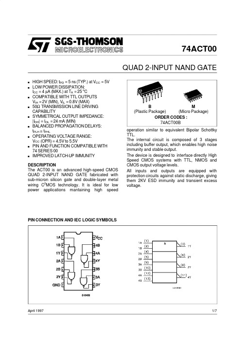
74ACT00QUAD 2-INPUT NAND GATEApril 1997s HIGH SPEED:t PD =5ns (TYP.)at V CC =5V sLOW POWER DISSIPATION:I CC =4µA (MAX.)at T A =25o CsCOMPATIBLE WITH TTL OUTPUTS V IH =2V (MIN),V IL =0.8V (MAX)s50ΩTRANSMISSION LINE DRIVING CAPABILITYsSYMMETRICAL OUTPUT IMPEDANCE:|I OH |=I OL =24mA (MIN)sBALANCED PROPAGATION DELAYS:t PLH ≅t PHLsOPERATING VOLTAGE RANGE:V CC (OPR)=4.5V to 5.5VsPIN AND FUNCTION COMPATIBLE WITH 74SERIES 00sIMPROVED LATCH-UP IMMUNITYDESCRIPTIONThe ACT00is an advanced high-speed CMOS QUAD 2-INPUT NAND GATE fabricated with sub-micron silicon gate and double-layer metal wiring C 2MOS technology.It is ideal for low power applications mantaining high speedoperation similar to equivalent Bipolar Schottky TTL.The internal circuit is composed of 3stages including buffer output,which enables high noise immunity and stable output.The device is designed to interface directly High Speed CMOS systems with TTL,NMOS and CMOS output voltage levels.All inputs and outputs are equipped with protection circuits against static discharge,giving them 2KV ESD immunity and transient excess voltage.PIN CONNECTION AND IEC LOGIC SYMBOLSORDER CODES :74ACT00B M(Micro Package)B (Plastic Package)1/7INPUT AND OUTPUT EQUIVALENT CIRCUITABSOLUTE MAXIMUM RATINGSSymbol ParameterValue Unit V CC Supply Voltage -0.5to +7V V I DC Input Voltage -0.5to V CC +0.5V V O DC Output Voltage -0.5to V CC +0.5V I IK DC Input Diode Current ±20mA I OK DC Output Diode Current ±20mA I O DC Output Current ±50mA I CC or I GND DC V CC or Ground Current±200mAT stg Storage Temperature -65to +150o C T LLead Temperature (10sec)300oCAbsolute Maximum Ratings are those values beyond which damage to the device may occur.Functional operation under these condition is not implied.TRUTH TABLEA B Y L L H L H H H L H HHLPIN DESCRIPTIONPIN No SYMBOL NAME AND FUNCTION 1,4,9,121A to 4A Data Inputs 2,5,10,131B to 4B Data Inputs 3,6,8,111Y to 4Y Data Outputs 7GND Ground (0V)14V CCPositive Supply VoltageRECOMMENDED OPERATING CONDITIONSSymbol ParameterValue Unit V CC Supply Voltage 4.5to 5.5V V I Input Voltage 0to V CC V V O Output Voltage0to V CC VT op Operating Temperature:-40to +85oCdt/dvInput Rise and Fall Time V CC =4.5to 5.5V (note 1)8ns/V1)V IN from 0.8V to 2.0V74ACT002/7CAPACITIVE CHARACTERISTICSSymbolParameterTest ConditionsValueUnitV CC (V)T A =25oC -40to 85oC Min.Typ.Max.Min.Max.C IN Input Capacitance 5.04pF C PDPower Dissipation Capacitance (note 1)5.031pF1)C PD isdefined as the value of the IC’s internal equivalent capacitance which is calculated from the operating current consumption without load.(Refer to Test Circuit).Ave rage operating current can be obtained by the following equation.I CC (opr)=C PD •V CC •f IN +I CC /n (per circuit)AC ELECTRICAL CHARACTERISTICS (C L =50pF,R L =500Ω,Input t r =t f =3ns)SymbolParameterTest ConditionValueUnitV CC (V)T A =25oC -40to 85o CMin.Typ.Max.Min.Max.t PLH t PHLPropagation Delay Time5.0(*)1.5 5.09.0 1.09.5ns(*)Voltage range is 5V ±0.5VDC SPECIFICATIONSSymbolParameterTest ConditionsValueUnitV CC (V)T A =25oC -40to 85oC Min.Typ.Max.Min.Max.V IH High Level Input Voltage 4.5V O =0.1V or V CC -0.1V 2.0 1.5 2.0V 5.5 2.01.52.0V IL Low Level Input Voltage 4.5V O =0.1V or V CC -0.1V 1.50.80.8V 5.5 1.50.80.8V OHHigh Level Output Voltage4.5V I (*)=V IH or V ILI O =-50µA 4.4 4.49 4.4V5.5I O =-50µA 5.4 5.495.44.5I O =-24mA 3.86 3.765.5I O =-24mA 4.864.76V OLLow Level Output Voltage4.5V I (*)=V IH or V ILI O =50µA 0.0010.10.1V5.5I O =50mA 0.0010.10.14.5I O =24mA 0.360.445.5I O =24mA0.360.44I I Input Leakage Current 5.5V I =V CC or GND ±0.1±1µA I CCT Max I CC /Input 5.5V I =V CC -2.1V 0.61.5mA I CC Quiescent Supply Current5.5V I =V CC or GND 440µA I OLD Dynamic Output Current (note 1,2)5.5V OLD =1.65V max 75mA I OHDV OHD =3.85V min-75mA1)Maximum test duration 2ms,one output loaded at time2)Incident wave switch ing is guaranteed on transmission lines with impe dances as low as 50Ω.(*)All outputs loaded.74ACT003/774ACT00TEST CIRCUITC L=50pF or equivalent(includes jig and probe capacitance)R L=R1=500Ωor equiva lentR T=Z OUT of pulse generator(typically50Ω)WAVEFORM:PROPAGATION DELAYS(f=1MHz;50%duty cycle) 4/7DIM.mminch MIN.TYP.MAX.MIN.TYP.MAX.a10.510.020B 1.391.650.0550.065b 0.50.020b10.250.010D 200.787E 8.50.335e 2.540.100e315.240.600F 7.10.280I 5.10.201L 3.30.130Z1.272.540.0500.100P001APlastic DIP14MECHANICAL DATA74ACT005/7DIM.mm inch MIN.TYP.MAX.MIN.TYP.MAX.A 1.750.068a10.10.20.0030.007a2 1.650.064b 0.350.460.0130.018b10.190.250.0070.010C 0.50.019c145(typ.)D 8.558.750.3360.344E 5.86.20.2280.244e 1.270.050e37.620.300F 3.8 4.00.1490.157G 4.6 5.30.1810.208L 0.5 1.270.0190.050M 0.680.026S8(max.)P013GSO14MECHANICAL DATA74ACT006/774ACT00 Information furnished is believed to be accurate and reliable.However,SGS-THOMSON Microelectronics assumes no responsabilit y for the consequences of use of such information nor for any infringemen t of patents or other rights of third parties which may results from its use.No license is granted by implication or otherwise under any patent or patent rights of SGS-THOMSON Microelectr onics.Specifications mention ed in this publication are subject to change without notice.This publication supersede s and replaces all information previously supplied.SGS-THOMSON Microelectr onics products are not auth orized for use as critical compon ents in life support devices or systems without expre ss written approval of SGS-THOMSON Microelectonics.©1997SGS-THOMSON Microelectronics-Printed in Italy-All Rights Reserve dSGS-THOMSON Microelectronics GROUP OF COMPANIESAustralia-Brazil-Canada-China-France-Germany-Hong Kong-Italy-Japan-Korea-Malaysia-Malta-Morocco-The Netherlands-Singapore-Spain-Sweden-Switzerland-Taiwan-Thailand-United Kingdom-U.S.A.7/7。
常用74系列标准数字电路的中文名称资料收藏常用74系列标准数字电路的中文名称资料器件代号器件名称74 74LS 74HC00 四2输入端与非门√√√01 四2输入端与非门(OC) √√02 四2输入端或非门√√√03 四2输入端与非门(OC) √√04 六反相器√√√05 六反相器(OC) √√06 六高压输出反相器(OC,30V) √√07 六高压输出缓冲,驱动器(OC,30V) √√√08 四2输入端与门√√√09 四2输入端与门(OC) √√√10 三3输入端与非门√√√11 三3输入端与门√√12 三3输入端与非门(OC) √√√13 双4输入端与非门√√√14 六反相器√√√15 三3输入端与门(OC) √√16 六高压输出反相器(OC,15V) √17 六高压输出缓冲,驱动器(OC,15V) √20 双4输入端与非门√√√21 双4输入端与门√√√22 双4输入端与非门(OC) √√25 双4输入端或非门(有选通端) √√√26 四2输入端高压输出与非缓冲器√√√27 三3输入端或非门√√√28 四2输入端或非缓冲器√√√器件代号器件名称74 74LS 74HC30 8输入端与非门√√√32 四2输入端或门√√√33 四2输入端或非缓冲器(OC) √√37 四2输入端与非缓冲器√√38 四2输入端与非缓冲器(OC) √√40 双4输入端与非缓冲器√√√42 4线-10线译码器(BCD输入) √√43 4线-10线译码器(余3码输入) √44 4线-10线译码器(余3葛莱码输入) √48 4线-7段译码器√49 4线-7段译码器√50 双2路2-2输入与或非门√√√51 2路3-3输入,2路2-2输入与或非门√√√52 4路2-3-2-2输入与或门√53 4路2-2-2-2输入与或非门√54 4路2-3-3-2输入与或非门√√55 2路4-4输入与或非门√60 双4输入与扩展器√√61 三3输入与扩展器√62 4路2-3-3-2输入与或扩展器√64 4路4-2-3-2输入与或非门√65 4路4-2-3-2输入与或非门(OC) √70 与门输入J-K触发器√71 与或门输入J-K触发器√72 与门输入J-K触发器√器件代号器件名称74 74LS 74HC74 双上升沿D型触发器√√78 双D型触发器√√85 四位数值比较器√86 四2输入端异或门√√√87 4位二进制原码/反码√95 4位移位寄存器√101 与或门输入J-K触发器√102 与门输入J-K触发器√107 双主-从J-K触发器√108 双主-从J-K触发器√74F74是高速的TTL芯片和74HC一样就是速度高109 双主-从J-K触发器√110 与门输入J-K触发器√111 双主-从J-K触发器√√112 双下降沿J-K触发器√113 双下降沿J-K触发器√114 双下降沿J-K触发器√116 双4位锁存器√120 双脉冲同步驱动器√121 单稳态触发器√√√122 可重触发单稳态触发器√√√123 可重触发双稳态触发器√√√125 四总线缓冲器√√√126 四总线缓冲器√√√128 四2输入端或非线驱动器√√√132 四2输入端与非门√√√d触发器芯片有:74HC74 74LS90 双D触发器74LS7474LS364八D触发器(三态)7474、74 H74、74F74、74ALS74、74L74、74LS74A、74S74、74HC73、74C74双D型正沿触发器(带预置和清除端)74174、74LS174、74F174、74ALS174、74S174、74HC174、74C174六D型触发器(带清除端)74175、74LS175、74F175、74ALS175、74S175、74HC175、74C175 四D型触发器(带清除端)74273、74LS273、74S273、74F273、74ALS273、74HC273 八D型触发器(带清除端)74LS364八D触发器(三态)74LS377、74F377、74S3777八D 触发器74LS378、74F378、74S378、74HC378六D 触发器74LS379、74F379、74S379、74HC379八D 触发器。

TECHNICAL DATAKK 74HC02AQuad 2-Input NOR GateThe KK 74HC02A is identical in pinout to the LS/ALS02. The device inputs are compatible with standard CMOS outputs; with pullup resistors, they are compatible with LS/ALSTTL outputs.• Outputs Directly Interface to CMOS, NMOS, and TTL • Operating Voltage Range: 2.0 to 6.0 V• Low Input Current: 1.0 µA • High Noise Immunity Characteristic of CMOS Devices LOGIC DIAGRAMPIN 14 =V CC PIN 7 = GNDPIN ASSIGNMENTFUNCTION TABLEInputs OutputA B Y L L H L H L H L L H H LMAXIMUM RATINGS*Symbol Parameter ValueUnit V CC DC Supply Voltage (Referenced to GND) -0.5 to +7.0 VV IN DC Input Voltage (Referenced to GND) -1.5 to V CC +1.5 VV OUT DC Output Voltage (Referenced to GND) -0.5 to V CC +0.5 VI IN DC Input Current, per Pin ±20 mAI OUT DC Output Current, per Pin ±25 mAI CC DC Supply Current, V CC and GND Pins ±50 mAP D Power Dissipation in Still Air, Plastic DIP* SOIC Package*750500mWTstg Storage Temperature -65 to +150 °CT L Lead Temperature, 1 mm from Case for 10 Seconds(Plastic DIP or SOIC Package)260 °C*Maximum Ratings are those values beyond which damage to the device may occur.Functional operation should be restricted to the Recommended Operating Conditions.**Derating - Plastic DIP: - 10 mW/°C from 65° to 125°CSOIC Package: : - 7 mW/°C from 65° to 125°CRECOMMENDED OPERATING CONDITIONSSymbol Parameter MinMaxUnit V CC DC Supply Voltage (Referenced to GND) 2.0 6.0 VV IN, V OUT DC Input Voltage, Output Voltage (Referenced to GND) 0 V CC VT A Operating Temperature, All Package Types -55 +125 °Ct r, t f Input Rise and Fall Time (Figure 1) V CC =2.0 VV CC =4.5 VV CC =6.0 V 01000500400nsThis device contains protection circuitry to guard against damage due to high static voltages or electric fields. However, precautions must be taken to avoid applications of any voltage higher than maximum rated voltages to this high-impedance circuit. For proper operation, V IN and V OUT should be constrained to the range GND≤(V IN or V OUT)≤V CC.Unused inputs must always be tied to an appropriate logic voltage level (e.g., either GND or V CC). Unused outputs must be left open.DC ELECTRICAL CHARACTERISTICS (Voltages Referenced to GND)Guaranteed Limit Symbol ParameterTest Conditions V CCV25 °Cto -55°C ≤85 °C ≤125 °C UnitV ILMaximum Low -Level Input Voltage V OUT =0.1 V or V CC =0.1 V I OUT ≤ 20 µА 2.0 4.5 6.0 0.5 1.351.8 0.5 1.35 1.8 0.5 1.35 1.8 V V IH Minimum High-Level Input Voltage V OUT =0.1 V or V CC =0.1 V I OUT ≤ 20 µА 2.0 4.5 6.0 1.5 3.154.2 1.5 3.15 4.2 1.5 3.15 4.2 VV IN =V IH or V IL I OUT ≤ 20 µA 2.0 4.5 6.00.1 0.1 0.10.1 0.1 0.10.1 0.1 0.1V IN =V IH or V IL I OUT ≤ 4.0 mA 4.5 0.260.33 0.4 V OL Maximum Low-Level Output VoltageV IN =V IH or V IL I OUT ≤ 5.2 mA6.0 0.260.33 0.4 VV IN =V IH or V IL I OUT ≤ 20 µA 2.0 4.5 6.01.9 4.4 5.91.9 4.4 5.91.9 4.4 5.9V IN =V IH or V IL I OUT ≤ 4.0 mA 4.5 3.98 3.84 3.7 V OHMinimum High-Level Output VoltageV IN =V IH or V IL I OUT ≤ 5.2 mA6.0 5.485.34 5.2VI IL Maximum Low-Level Input Leakage Current V IL =GND 6.0 -0.1 -1.0 -1.0 µA I IH Maximum High-Level Input Leakage Current V IH =V CC 6.0 0.1 1.0 1.0 µA I CCMaximum Quiescent Supply Current (per Package)V IL =V CC V IH =GND I OUT =0 µA6.0 1.0 10 40 µAAC ELECTRICAL CHARACTERISTICSGuaranteed Limit Symbol ParameterTest Conditions V CC V25 °Cto -55°C ≤85°C≤125°CUnitt PLH , t PHLMaximum Propagation Delay, Input A or B to Output Y (Figures 1 and 2)V IL =0 V V IH =V CCt LH =t HL =6 ns C L = 50 pF 2.04.56.080 16 14 100 20 17 120 24 20 nst TLH , t THL Maximum Output Transition Time, Any Output (Figures 1 and 2)V IL =0 V V IH =V CCt LH =t HL =6 ns C L = 50 pF 2.04.56.075 15 13 95 19 16 110 22 19 nsC IN Maximum Input Capacitance6.0101010pF ТА = 25°C,V CC =5.0 VC PDPower Dissipation Capacitance (Per Gate) Used to determine the no-load dynamic power consumption:P D =C PD V CC 2f+I CC V CC5.022pFFigure 1. Switching Waveforms Figure 2. Test CircuitEXPANDED LOGIC DIAGRAM(1/4 of the Device)。

常用74系列芯片功能速查技术天地 2008-08-10 09:10 阅读1148 评论0字号:大中小7400 TTL 2输入端四与非门7401 TTL 集电极开路2输入端四与非门7402 TTL 2输入端四或非门7403 TTL 集电极开路2输入端四与非门7404 TTL 六反相器7405 TTL 集电极开路六反相器7406 TTL 集电极开路六反相高压驱动器7407 TTL 集电极开路六正相高压驱动器7408 TTL 2输入端四与门7409 TTL 集电极开路2输入端四与门7410 TTL 3输入端3与非门74107 TTL 带清除主从双J-K触发器74109 TTL 带预置清除正触发双J-K触发器7411 TTL 3输入端3与门74112 TTL 带预置清除负触发双J-K触发器7412 TTL 开路输出3输入端三与非门74121 TTL 单稳态多谐振荡器74122 TTL 可再触发单稳态多谐振荡器74123 TTL 双可再触发单稳态多谐振荡器74125 TTL 三态输出高有效四总线缓冲门74126 TTL 三态输出低有效四总线缓冲门7413 TTL 4输入端双与非施密特触发器74132 TTL 2输入端四与非施密特触发器74133 TTL 13输入端与非门74136 TTL 四异或门74138 TTL 3-8线译码器/复工器74139 TTL 双2-4线译码器/复工器7414 TTL 六反相施密特触发器74145 TTL BCD—十进制译码/驱动器7415 TTL 开路输出3输入端三与门74150 TTL 16选1数据选择/多路开关74151 TTL 8选1数据选择器74153 TTL 双4选1数据选择器74154 TTL 4线—16线译码器74155 TTL 图腾柱输出译码器/分配器74156 TTL 开路输出译码器/分配器74157 TTL 同相输出四2选1数据选择器74158 TTL 反相输出四2选1数据选择器7416 TTL 开路输出六反相缓冲/驱动器74160 TTL 可预置BCD异步清除计数器74161 TTL 可予制四位二进制异步清除计数器74162 TTL 可预置BCD同步清除计数器74163 TTL 可予制四位二进制同步清除计数器74164 TTL 八位串行入/并行输出移位寄存器74165 TTL 八位并行入/串行输出移位寄存器74166 TTL 八位并入/串出移位寄存器74169 TTL 二进制四位加/减同步计数器7417 TTL 开路输出六同相缓冲/驱动器74170 TTL 开路输出4×4寄存器堆74173 TTL 三态输出四位D型寄存器74174 TTL 带公共时钟和复位六D触发器74175 TTL 带公共时钟和复位四D触发器74180 TTL 9位奇数/偶数发生器/校验器74181 TTL 算术逻辑单元/函数发生器74185 TTL 二进制—BCD代码转换器74190 TTL BCD同步加/减计数器74191 TTL 二进制同步可逆计数器74192 TTL 可预置BCD双时钟可逆计数器74193 TTL 可预置四位二进制双时钟可逆计数器74194 TTL 四位双向通用移位寄存器74195 TTL 四位并行通道移位寄存器74196 TTL 十进制/二-十进制可预置计数锁存器74197 TTL 二进制可预置锁存器/计数器7420 TTL 4输入端双与非门7421 TTL 4输入端双与门7422 TTL 开路输出4输入端双与非门74221 TTL 双/单稳态多谐振荡器74240 TTL 八反相三态缓冲器/线驱动器74241 TTL 八同相三态缓冲器/线驱动器74243 TTL 四同相三态总线收发器74244 TTL 八同相三态缓冲器/线驱动器74245 TTL 八同相三态总线收发器74247 TTL BCD—7段15V输出译码/驱动器74248 TTL BCD—7段译码/升压输出驱动器74249 TTL BCD—7段译码/开路输出驱动器74251 TTL 三态输出8选1数据选择器/复工器74253 TTL 三态输出双4选1数据选择器/复工器74256 TTL 双四位可寻址锁存器74257 TTL 三态原码四2选1数据选择器/复工器74258 TTL 三态反码四2选1数据选择器/复工器74259 TTL 八位可寻址锁存器/3-8线译码器7426 TTL 2输入端高压接口四与非门74260 TTL 5输入端双或非门74266 TTL 2输入端四异或非门7427 TTL 3输入端三或非门74273 TTL 带公共时钟复位八D触发器74279 TTL 四图腾柱输出S-R锁存器7428 TTL 2输入端四或非门缓冲器74283 TTL 4位二进制全加器74290 TTL 二/五分频十进制计数器74293 TTL 二/八分频四位二进制计数器74295 TTL 四位双向通用移位寄存器74298 TTL 四2输入多路带存贮开关74299 TTL 三态输出八位通用移位寄存器7430 TTL 8输入端与非门7432 TTL 2输入端四或门74322 TTL 带符号扩展端八位移位寄存器74323 TTL 三态输出八位双向移位/存贮寄存器7433 TTL 开路输出2输入端四或非缓冲器74347 TTL BCD—7段译码器/驱动器74352 TTL 双4选1数据选择器/复工器74353 TTL 三态输出双4选1数据选择器/复工器74365 TTL 门使能输入三态输出六同相线驱动器74365 TTL 门使能输入三态输出六同相线驱动器74366 TTL 门使能输入三态输出六反相线驱动器74367 TTL 4/2线使能输入三态六同相线驱动器74368 TTL 4/2线使能输入三态六反相线驱动器7437 TTL 开路输出2输入端四与非缓冲器74373 TTL 三态同相八D锁存器74374 TTL 三态反相八D锁存器74375 TTL 4位双稳态锁存器74377 TTL 单边输出公共使能八D锁存器74378 TTL 单边输出公共使能六D锁存器74379 TTL 双边输出公共使能四D锁存器7438 TTL 开路输出2输入端四与非缓冲器74380 TTL 多功能八进制寄存器7439 TTL 开路输出2输入端四与非缓冲器74390 TTL 双十进制计数器74393 TTL 双四位二进制计数器7440 TTL 4输入端双与非缓冲器7442 TTL BCD—十进制代码转换器74352 TTL 双4选1数据选择器/复工器74353 TTL 三态输出双4选1数据选择器/复工器74365 TTL 门使能输入三态输出六同相线驱动器74366 TTL 门使能输入三态输出六反相线驱动器74367 TTL 4/2线使能输入三态六同相线驱动器74368 TTL 4/2线使能输入三态六反相线驱动器7437 TTL 开路输出2输入端四与非缓冲器74373 TTL 三态同相八D锁存器74374 TTL 三态反相八D锁存器74375 TTL 4位双稳态锁存器74377 TTL 单边输出公共使能八D锁存器74378 TTL 单边输出公共使能六D锁存器74379 TTL 双边输出公共使能四D锁存器7438 TTL 开路输出2输入端四与非缓冲器74380 TTL 多功能八进制寄存器7439 TTL 开路输出2输入端四与非缓冲器74390 TTL 双十进制计数器74393 TTL 双四位二进制计数器7440 TTL 4输入端双与非缓冲器7442 TTL BCD—十进制代码转换器74447 TTL BCD—7段译码器/驱动器7445 TTL BCD—十进制代码转换/驱动器74450 TTL 16:1多路转接复用器多工器74451 TTL 双8:1多路转接复用器多工器74453 TTL 四4:1多路转接复用器多工器7446 TTL BCD—7段低有效译码/驱动器74460 TTL 十位比较器74461 TTL 八进制计数器74465 TTL 三态同相2与使能端八总线缓冲器74466 TTL 三态反相2与使能八总线缓冲器74467 TTL 三态同相2使能端八总线缓冲器74468 TTL 三态反相2使能端八总线缓冲器74469 TTL 八位双向计数器7447 TTL BCD—7段高有效译码/驱动器7448 TTL BCD—7段译码器/内部上拉输出驱动74490 TTL 双十进制计数器74491 TTL 十位计数器74498 TTL 八进制移位寄存器7450 TTL 2-3/2-2输入端双与或非门74502 TTL 八位逐次逼近寄存器74503 TTL 八位逐次逼近寄存器7451 TTL 2-3/2-2输入端双与或非门74533 TTL 三态反相八D锁存器74534 TTL 三态反相八D锁存器7454 TTL 四路输入与或非门74540 TTL 八位三态反相输出总线缓冲器7455 TTL 4输入端二路输入与或非门74563 TTL 八位三态反相输出触发器74564 TTL 八位三态反相输出D触发器74573 TTL 八位三态输出触发器74574 TTL 八位三态输出D触发器74645 TTL 三态输出八同相总线传送接收器74670 TTL 三态输出4×4寄存器堆7473 TTL 带清除负触发双J-K触发器7474 TTL 带置位复位正触发双D触发器7476 TTL 带预置清除双J-K触发器7483 TTL 四位二进制快速进位全加器7485 TTL 四位数字比较器7486 TTL 2输入端四异或门7490 TTL 可二/五分频十进制计数器7493 TTL 可二/八分频二进制计数器7495 TTL 四位并行输入\输出移位寄存器7497 TTL 6位同步二进制乘法器常用74系列标准数字电路的中文名称资料器件代号器件名称74 74LS 74HC00 四2输入端与非门√ √ √01 四2输入端与非门(OC) √ √02 四2输入端或非门√ √ √03 四2输入端与非门(OC) √ √04 六反相器√ √ √05 六反相器(OC) √ √06 六高压输出反相器(OC,30V) √ √07 六高压输出缓冲,驱动器(OC,30V) √ √ √08 四2输入端与门√ √ √09 四2输入端与门(OC) √√ √10 三3输入端与非门√ √ √11 三3输入端与门√ √12 三3输入端与非门(OC) √ √ √13 双4输入端与非门√ √ √14 六反相器√ √ √15 三3输入端与门(OC) √ √16 六高压输出反相器(OC,15V) √17 六高压输出缓冲,驱动器(OC,15V) √20 双4输入端与非门√ √ √21 双4输入端与门√ √ √22 双4输入端与非门(OC) √ √25 双4输入端或非门(有选通端) √ √ √26 四2输入端高压输出与非缓冲器√ √ √27 三3输入端或非门√ √ √28 四2输入端或非缓冲器√ √ √30 8输入端与非门√ √ √32 四2输入端或门√ √ √33 四2输入端或非缓冲器(OC) √ √37 四2输入端与非缓冲器√ √38 四2输入端与非缓冲器(OC) √ √40 双4输入端与非缓冲器√ √ √42 4线-10线译码器(BCD输入) √ √43 4线-10线译码器(余3码输入) √44 4线-10线译码器(余3葛莱码输入) √48 4线-7段译码器√49 4线-7段译码器√50 双2路2-2输入与或非门√ √ √51 2路3-3输入,2路2-2输入与或非门√ √ √52 4路2-3-2-2输入与或门√53 4路2-2-2-2输入与或非门√54 4路2-3-3-2输入与或非门√ √55 2路4-4输入与或非门√60 双4输入与扩展器√ √61 三3输入与扩展器√62 4路2-3-3-2输入与或扩展器√64 4路4-2-3-2输入与或非门√65 4路4-2-3-2输入与或非门(OC) √70 与门输入J-K触发器√71 与或门输入J-K触发器√72 与门输入J-K触发器√74 双上升沿D型触发器√ √78 双D型触发器√ √85 四位数值比较器√86 四2输入端异或门√ √ √87 4位二进制原码/反码√95 4位移位寄存器√101 与或门输入J-K触发器√102 与门输入J-K触发器√107 双主-从J-K触发器√108 双主-从J-K触发器√109 双主-从J-K触发器√110 与门输入J-K触发器√111 双主-从J-K触发器√ √112 双下降沿J-K触发器√113 双下降沿J-K触发器√114 双下降沿J-K触发器√116 双4位锁存器√120 双脉冲同步驱动器√121 单稳态触发器√ √ √122 可重触发单稳态触发器√ √ √123 可重触发双稳态触发器√ √ √125 四总线缓冲器√ √ √126 四总线缓冲器√ √ √128 四2输入端或非线驱动器√ √ √132 四2输入端与非门√ √ √。

PACKAGING INFORMATIONOrderable Device Status (1)Package Type Package Drawing Pins Package Qty Eco Plan (2)Lead/Ball FinishMSL Peak Temp (3)5962-8752501M2A ACTIVE LCCC FK 201TBD POST-PLATE N /A for Pkg Type 5962-8752501MCA ACTIVE CDIP J 141TBD A42SNPB N /A for Pkg Type 5962-8752501MDA ACTIVE CFP W 141TBD A42N /A for Pkg Type SN74ACT74D ACTIVE SOIC D 1450Green (RoHS &no Sb/Br)CU NIPDAU Level-1-260C-UNLIM SN74ACT74DBLE OBSOLETE SSOP DB 14TBDCall TI Call TISN74ACT74DBR ACTIVE SSOP DB 142000Green (RoHS &no Sb/Br)CU NIPDAU Level-1-260C-UNLIM SN74ACT74DBRE4ACTIVE SSOP DB142000Green (RoHS &no Sb/Br)CU NIPDAU Level-1-260C-UNLIM SN74ACT74DE4ACTIVE SOIC D 1450Green (RoHS &no Sb/Br)CU NIPDAU Level-1-260C-UNLIM SN74ACT74DR ACTIVE SOIC D 142500Green (RoHS &no Sb/Br)CU NIPDAU Level-1-260C-UNLIM SN74ACT74DRE4ACTIVE SOIC D 142500Green (RoHS &no Sb/Br)CU NIPDAU Level-1-260C-UNLIM SN74ACT74N ACTIVE PDIP N 1425Pb-Free (RoHS)CU NIPDAU N /A for Pkg Type SN74ACT74NE4ACTIVE PDIP N 1425Pb-Free (RoHS)CU NIPDAU N /A for Pkg Type SN74ACT74NSR ACTIVE SO NS 142000Green (RoHS &no Sb/Br)CU NIPDAU Level-1-260C-UNLIM SN74ACT74NSRE4ACTIVE SO NS 142000Green (RoHS &no Sb/Br)CU NIPDAU Level-1-260C-UNLIM SN74ACT74PW ACTIVE TSSOP PW 1490Green (RoHS &no Sb/Br)CU NIPDAU Level-1-260C-UNLIM SN74ACT74PWE4ACTIVE TSSOP PW 1490Green (RoHS &no Sb/Br)CU NIPDAU Level-1-260C-UNLIM SN74ACT74PWLE OBSOLETE TSSOP PW 14TBDCall TI Call TISN74ACT74PWR ACTIVE TSSOP PW 142000Green (RoHS &no Sb/Br)CU NIPDAU Level-1-260C-UNLIM SN74ACT74PWRE4ACTIVE TSSOP PW 142000Green (RoHS &no Sb/Br)CU NIPDAULevel-1-260C-UNLIMSNJ54ACT74FK ACTIVE LCCC FK 201TBD POST-PLATE N /A for Pkg Type SNJ54ACT74J ACTIVE CDIP J 141TBD A42SNPB N /A for Pkg Type SNJ54ACT74WACTIVECFPW141TBDA42N /A for Pkg Type(1)The marketing status values are defined as follows:ACTIVE:Product device recommended for new designs.LIFEBUY:TI has announced that the device will be discontinued,and a lifetime-buy period is in effect.NRND:Not recommended for new designs.Device is in production to support existing customers,but TI does not recommend using this part in a new design.PREVIEW:Device has been announced but is not in production.Samples may or may not be available.OBSOLETE:TI has discontinued the production of the device.(2)Eco Plan -The planned eco-friendly classification:Pb-Free (RoHS),Pb-Free (RoHS Exempt),or Green (RoHS &no Sb/Br)-please check /productcontent for the latest availability information and additional product content details.TBD:The Pb-Free/Green conversion plan has not been defined.Pb-Free (RoHS):TI's terms "Lead-Free"or "Pb-Free"mean semiconductor products that are compatible with the current RoHS requirements for all 6substances,including the requirement that lead not exceed 0.1%by weight in homogeneous materials.Where designed to be soldered18-Jul-2006at high temperatures,TI Pb-Free products are suitable for use in specified lead-free processes.Pb-Free (RoHS Exempt):This component has a RoHS exemption for either 1)lead-based flip-chip solder bumps used between the die and package,or 2)lead-based die adhesive used between the die and leadframe.The component is otherwise considered Pb-Free (RoHS compatible)as defined above.Green (RoHS &no Sb/Br):TI defines "Green"to mean Pb-Free (RoHS compatible),and free of Bromine (Br)and Antimony (Sb)based flame retardants (Br or Sb do not exceed 0.1%by weight in homogeneous material)(3)MSL,Peak Temp.--The Moisture Sensitivity Level rating according to the JEDEC industry standard classifications,and peak solder temperature.Important Information and Disclaimer:The information provided on this page represents TI's knowledge and belief as of the date that it is provided.TI bases its knowledge and belief on information provided by third parties,and makes no representation or warranty as to the accuracy of such information.Efforts are underway to better integrate information from third parties.TI has taken and continues to take reasonable steps to provide representative and accurate information but may not have conducted destructive testing or chemical analysis on incoming materials and chemicals.TI and TI suppliers consider certain information to be proprietary,and thus CAS numbers and other limited information may not be available for release.In no event shall TI's liability arising out of such information exceed the total purchase price of the TI part(s)at issue in this document sold by TI to Customer on an annualbasis.18-Jul-2006IMPORTANT NOTICETexas Instruments Incorporated and its subsidiaries (TI) reserve the right to make corrections, modifications, enhancements, improvements, and other changes to its products and services at any time and to discontinue any product or service without notice. Customers should obtain the latest relevant information before placing orders and should verify that such information is current and complete. All products are sold subject to TI’s terms and conditions of sale supplied at the time of order acknowledgment.TI warrants performance of its hardware products to the specifications applicable at the time of sale in accordance with TI’s standard warranty. T esting and other quality control techniques are used to the extent TI deems necessary to support this warranty. Except where mandated by government requirements, testing of all parameters of each product is not necessarily performed.TI assumes no liability for applications assistance or customer product design. Customers are responsible for their products and applications using TI components. T o minimize the risks associated with customer products and applications, customers should provide adequate design and operating safeguards.TI does not warrant or represent that any license, either express or implied, is granted under any TI patent right, copyright, mask work right, or other TI intellectual property right relating to any combination, machine, or process in which TI products or services are used. Information published by TI regarding third-party products or services does not constitute a license from TI to use such products or services or a warranty or endorsement thereof. Use of such information may require a license from a third party under the patents or other intellectual property of the third party, or a license from TI under the patents or other intellectual property of TI.Reproduction of information in TI data books or data sheets is permissible only if reproduction is without alteration and is accompanied by all associated warranties, conditions, limitations, and notices. Reproduction of this information with alteration is an unfair and deceptive business practice. TI is not responsible or liable for such altered documentation.Resale of TI products or services with statements different from or beyond the parameters stated by TI for that product or service voids all express and any implied warranties for the associated TI product or service and is an unfair and deceptive business practice. TI is not responsible or liable for any such statements. Following are URLs where you can obtain information on other Texas Instruments products and application solutions:Products ApplicationsAmplifiers Audio /audioData Converters Automotive /automotiveDSP Broadband /broadbandInterface Digital Control /digitalcontrolLogic Military /militaryPower Mgmt Optical Networking /opticalnetwork Microcontrollers Security /securityLow Power Wireless /lpw Telephony /telephonyVideo & Imaging /videoWireless /wirelessMailing Address:Texas InstrumentsPost Office Box 655303 Dallas, Texas 75265Copyright 2006, Texas Instruments Incorporated。


TL F 989454ACT 74ACT8239-Bit D Flip-FlopMarch 199354ACT 74ACT8239-Bit D Flip-FlopGeneral DescriptionThe ’ACT823is a 9-bit buffered register It features Clock Enable and Clear which are ideal for parity bus interfacing in high performance microprogramming systems The ’ACT823offers noninverting outputs and is fully compatible with AMD’s Am29823FeaturesY Outputs source sink 24mAY TRI-STATE outputs for bus interfacing Y Inputs and outputs are on opposite sides Y’ACT823has TTL-compatible inputsLogic SymbolsConnection DiagramsTL F 9894–1IEEE IECTL F 9894–2Pin Assignmentfor DIP Flatpak and SOICTL F 9894–3Pin Assignmentfor LCCTL F 9894–4Pin Names Description D 0–D 8Data Inputs O 0–O 8Data Outputs OE Output Enable CLR ClearCP Clock Input ENClock EnableFACT TM is a trademark of National Semiconductor CorporationTRI-STATE is a registered trademark of National Semiconductor Corporation C 1995National Semiconductor CorporationRRD-B30M75 Printed in U S AFunctional DescriptionThe’ACT823consists of nine D-type edge-triggered flip-flops These have TRI-STATE outputs for bus systems or-ganized with inputs and outputs on opposite sides The buff-ered clock(CP)and buffered Output Enable(OE)are com-mon to all flip-flops The flip-flops will store the state of their individual D inputs that meet the setup and hold time re-quirements on the LOW-to-HIGH CP transition With OE LOW the contents of the flip-flops are available at the out-puts When OE is HIGH the outputs go to the high imped-ance state Operation of the OE input does not affect the state of the flip-flops In addition to the Clock and Output Enable pins there are Clear(CLR)and Clock Enable(EN) pins These devices are ideal for parity bus interfacing in high performance systemsWhen CLR is LOW and OE is LOW the outputs are LOW When CLR is HIGH data can be entered into the flip-flops When EN is LOW data on the inputs is transferred to the outputs on the LOW-to-HIGH clock transition When the EN is HIGH the outputs do not change state regardless of the data or clock input transitionsFunction TableInputs Internal OutputFunction OE CLR EN CP D Q OH X L L L L Z High ZH X L L H H Z High ZH L X X X L Z ClearL L X X X L L ClearH H H X X NC Z HoldL H H X X NC NC HoldH H L L L L Z LoadH H L L H H Z LoadL H L L L L L LoadL H L L H H H LoadH e HIGH Voltage LevelL e LOW Voltage LevelX e ImmaterialZ e High ImpedanceL e LOW-to-HIGH TransitionNC e No ChangeLogic DiagramTL F 9894–5 Please note that this diagram is provided only for the understanding of logic operations and should not be used to estimate propagation delays2Absolute Maximum Ratings(Note1)If Military Aerospace specified devices are required please contact the National Semiconductor Sales Office Distributors for availability and specifications Supply Voltage(V CC)b0 5V to7 0V DC Input Diode Current(I IK)V I e b0 5V b20mA V I e V CC a0 5V a20mA DC Input Voltage(V I)b0 5V to V CC a0 5V DC Output Diode Current(I OK)V O e b0 5V b20mA V O e V CC a0 5V a20mA DC Output Voltage(V O)b0 5V to V CC a0 5V DC Output Source or Sink Current(I O)g50mA DC V CC or Ground Currentper Output Pin(I CC or I GND)g50mA Storage Temperature(T STG)b65 C to a150 C Junction Temperature(T J)CDIP175 C PDIP140 C Note1 Absolute maximum ratings are those values beyond which damage to the device may occur The databook specifications should be met without exception to ensure that the system design is reliable over its power supply temperature and output input loading variables National does not recom-mend operation of FACT TM circuits outside databook specifications Recommended Operating ConditionsSupply Voltage(V CC)’ACT4 5V to5 5V Input Voltage(V I)0V to V CC Output Voltage(V O)0V to V CC Operating Temperature(T A)74ACT b40 C to a85 C 54ACT b55 C to a125 C Minimum Input Edge Rate(D V D t)’ACT DevicesV IN from0 8V to2 0VV CC 4 5V 5 5V125mV nsDC Electrical Characteristics74ACT54ACT74ACTSymbol Parameter V CCT A e25 C T Ae T A eUnits Conditions (V)b55 C to a125 C b40 C to a85 CTyp Guaranteed LimitsV IH Minimum High Level4 51 52 02 02 0V V OUT e0 1VInput Voltage5 51 52 02 02 0or V CC b0 1VV IL Maximum Low Level4 51 50 80 80 8V V OUT e0 1VInput Voltage4 51 50 80 80 8or V CC b0 1VV OH Minimum High Level4 54 494 44 44 4V I OUT e b50m A5 495 45 45 4V IN e V IL or V IH4 53 863 703 76V I OH b24mA4 864 704 76b24mAV OL Maximum Low Level4 50 0010 10 10 1V I OUT e50m AOutput Voltage5 50 0010 10 10 1V IN e V IL or V IH4 50 360 500 44V I OL24mA5 50 360 500 4424mAI IN Maximum Input5 5g0 1g1 0g1 0m A V I e V CC GNDLeakage CurrentI OZ Maximum TRI-STATE Current5 5g0 5g10 0g5 0m A V I e V IL V IHV O e V CC GNDI CCT Maximum I CC Input5 50 61 61 5mA V I e V CC b2 1VI OLD Minimum Dynamic5 55075mA V OLD e1 65V Max I OHD Output Current5 5b50b75mA V OHD e3 85V MinI CC Maximum Quiescent5 58 016080m A V IN e V CCSupply Current or GNDAll outputs loaded thresholds on input associated with output under testMaximum test duration2 0ms one output loaded at a timeNote I CC limit for54ACT 25 C is identical to74ACT 25 C3AC Electrical Characteristics74ACT54ACT74ACTT A e a25 C T A e b55 C T A e b40 CSymbol Parameter V CCC L e50pF to a125 C to a85 C Units(V)C L e50pF C L e50pFMin Typ Max Min Max Min Maxf max Maximum Clock5 012015895109MHzFrequencyt PLH Propagation Delay5 01 55 59 51 512 01 510 5nsCP to O nt PHL Propagation Delay5 02 05 59 51 512 01 510 5nsCP to O nt PHL Propagation Delay5 02 58 013 51 518 02 015 5nsCLR to O nt PZH Output Enable Time5 01 56 010 51 511 51 511 5nsOE to O nt PZL Output Enable Time5 02 06 511 01 512 01 512 0nsOE to O nt PHZ Output Disable Time5 01 56 511 01 513 51 512 0nsOE to O nt PLZ Output Disable Time5 01 56 010 51 512 01 511 5nsOE to O nVoltage Range5 0is5 0V g0 5VAC Operating Requirements74ACT54ACT74ACTT A e a25 C T A e b55 C T A e b40 CSymbol Parameter V CCC L e50pFto a125 C to a85 C Units (V)C L e50pF C L e50pFTyp Guaranteed Minimumt s Setup Time HIGH or LOW5 00 52 54 02 5nsD to CPt h Hold Time HIGH or LOW5 002 53 02 5nsD n to CPt s Setup Time HIGH or LOW5 002 04 02 5nsEN to CPt h Hold Time HIGH or LOW5 001 03 01 0nsEN to CPt w CP Pulse Width5 02 54 56 05 5nsHIGH or LOWt w CLR Pulse Width LOW5 03 05 57 05 5nst rec CLR to CP5 01 53 54 54 0nsRecovery TimeVoltage Range5 0is5 0V g0 5VCapacitanceSymbol Parameter Typ Units ConditionsC IN Input Capacitance4 5pF V CC e OPENC PD Power Dissipation44pF V CC e5 0VCapacitance4Ordering InformationThe device number is used to form part of a simplified purchasing code where the package type and temperature range are defined as follows74ACT823P C QRTemperature Range Family Special Variations74ACT e Commercial TTL-Compatible X e Devices shipped in13 reels54ACT e Military TTL-Compatible QR e Commercial grade device withburn-inDevice Type QB e Military grade device withenvironmental and burn-in Package Codeprocessing shipped in tubes SP e Slim Plastic DIPSD e Slim Ceramic DIP Temperature RangeF e Flatpak C e Commercial(b40 C to a85 C)L e Leadless Ceramic Chip Carrier(LCC)M e Military(b55 C to a125 C)S e Small Outline(SOIC)Physical Dimensions inches(millimeters)28Terminal Ceramic Leadless Chip Carrier(L)NS Package Number E28A5Physical Dimensions inches(millimeters)(Continued)24Lead Slim(0 300 Wide)Ceramic Dual-In-Line(SD)NS Package Number J24F24Lead Small Outline Integrated Circuit(S)NS Package Number M24B6Physical Dimensions inches(millimeters)(Continued)24Lead Slim(0 300 Wide)Plastic Dual-In-Line(SP)NS Package Number N24C754A C T 74A C T 8239-B i t D F l i p -F l o pPhysical Dimensions inches (millimeters)(Continued)Lit 11463524Lead Ceramic Flatpak (F)NS Package Number W24CLIFE SUPPORT POLICYNATIONAL’S PRODUCTS ARE NOT AUTHORIZED FOR USE AS CRITICAL COMPONENTS IN LIFE SUPPORT DEVICES OR SYSTEMS WITHOUT THE EXPRESS WRITTEN APPROVAL OF THE PRESIDENT OF NATIONAL SEMICONDUCTOR CORPORATION As used herein 1 Life support devices or systems are devices or 2 A critical component is any component of a life systems which (a)are intended for surgical implant support device or system whose failure to perform can into the body or (b)support or sustain life and whose be reasonably expected to cause the failure of the life failure to perform when properly used in accordance support device or system or to affect its safety or with instructions for use provided in the labeling can effectivenessbe reasonably expected to result in a significant injury to the userNational Semiconductor National Semiconductor National Semiconductor National Semiconductor National Semiconductores National Semiconductor CorporationGmbHJapan LtdHong Kong LtdDo Brazil Ltda(Australia)Pty Ltd 2900Semiconductor DriveLivry-Gargan-Str 10Sumitomo Chemical13th Floor Straight Block Rue Deputado Lacorda Franco Building 16。
TECHNICAL DATAKK 74ACT20Dual 4-Input NAND GateHigh-Speed Silicon-Gate CMOSThe KK 74ACT20 is identical in pinout to the LS/ALS20, HC/HCT20. The KK 74ACT20 may be used as a level converter for interfacing TTL or NMOS outputs to High Speed CMOS inputs. • TTL/NMOS Compatible Input Levels• Outputs Directly Interface to CMOS, NMOS, and TTL • Operating Voltage Range: 4.5 to 5.5 V• Low Input Current: 1.0 µA; 0.1 µA @ 25°C • Outputs Source/Sink 24 mALOGIC DIAGRAMPIN 14 =V CC PIN 7 = GNDPINS 3,11 = NO CONNECTIONPIN ASSIGNMENTNC = NO CONNECTIONFUNCTION TABLEInputs OutputA B C D Y L X X X H X L X X H X X L X H X X X L H H H H H LX = don’t careMAXIMUM RATINGS*Symbol Parameter ValueUnit V CC DC Supply Voltage (Referenced to GND) -0.5 to +7.0 VV IN DC Input Voltage (Referenced to GND) -0.5 to V CC +0.5 VV OUT DC Output Voltage (Referenced to GND) -0.5 to V CC +0.5 VI IN DC Input Current, per Pin ±20 mAI OUT DC Output Sink/Source Current, per Pin ±50 mAI CC DC Supply Current, V CC and GND Pins ±50 mAP D Power Dissipation in Still Air, Plastic DIP+ SOIC Package+ 750500mWTstg Storage Temperature -65 to +150 °CT L Lead Temperature, 1 mm from Case for 10 Seconds(Plastic DIP or SOIC Package)260 °C*Maximum Ratings are those values beyond which damage to the device may occur.Functional operation should be restricted to the Recommended Operating Conditions.+Derating - Plastic DIP: - 10 mW/°C from 65° to 125°CSOIC Package: : - 7 mW/°C from 65° to 125°CRECOMMENDED OPERATING CONDITIONSSymbol Parameter MinMaxUnit V CC DC Supply Voltage (Referenced to GND) 4.5 5.5 VV IN, V OUT DC Input Voltage, Output Voltage (Referenced to GND) 0 V CC VT J Junction Temperature (PDIP) 140 °CT A Operating Temperature, All Package Types -40 +85 °CI OH Output Current - High -24 mAI OL Output Current - Low 24 mAt r, t f Input Rise and Fall Time *(except Schmitt Inputs) V CC =4.5 VV CC =5.5 V108.0ns/V* VINfrom 0.8 V to 2.0 VThis device contains protection circuitry to guard against damage due to high static voltages or electric fields. However, precautions must be taken to avoid applications of any voltage higher than maximum rated voltages to this high-impedance circuit. For proper operation, V IN and V OUT should be constrained to the range GND≤(V IN or V OUT)≤V CC.Unused inputs must always be tied to an appropriate logic voltage level (e.g., either GND or V CC). Unused outputs must be left open.DC ELECTRICAL CHARACTERISTICS (Voltages Referenced to GND)V CC Guaranteed Limits Symbol Parameter TestConditions V25 °C -40°C to85°CUnitV IH Minimum High-Level Input Voltage V OUT=0.1 V or V CC-0.1 V 4.55.52.02.02.02.0VV IL Maximum Low -Level Input Voltage V OUT=0.1 V or V CC-0.1 V 4.55.50.80.80.80.8VV OH Minimum High-Level Output Voltage I OUT≤ -50 µA 4.55.54.45.44.45.4V*VIN=V IH or V ILI OH=-24 mAI OH=-24 mA4.55.53.864.863.764.76V OL Maximum Low-Level Output Voltage I OUT≤ 50 µA 4.55.50.10.10.10.1V*VIN=V IHI OL=24 mAI OL=24 mA4.55.50.360.360.440.44I IN Maximum InputLeakage CurrentV IN=V CC or GND 5.5±0.1 ±1.0 µA∆I CCT Additional MaxI CC/InputV IN=V CC - 2.1 V 5.5 1.5 mAI OLD+Minimum DynamicOutput CurrentV OLD=1.65 V Max 5.575 mAI OHD+Minimum DynamicOutput CurrentV OHD=3.85 V Min 5.5-75 mAI CC Maximum QuiescentSupply Current(per Package)V IN=V CC or GND 5.5 4.0 40 µA* All outputs loaded; thresholds on input associated with output under test.+Maximum test duration 2.0 ms, one output loaded at a time.AC ELECTRICAL CHARACTERISTICS (V CC=5.0 V ± 10%, C L=50pF,Input t r=t f=3.0 ns)LimitsGuaranteed Symbol Parameter 25 °C -40°C toUnit85°CMin Max MinMax2.0 9.0 1.5 10.5 nst PLH Propagation Delay, Input A , B, C or D to Output Y(Figure 1)2.0 9.0 1.5 10.5 nst PHL Propagation Delay, Input A , B, C or D to Output Y(Figure 1)C IN Maximum Input Capacitance 4.5 4.5 pFTypical @25°C,V CC=5.0 VC PD Power Dissipation Capacitance 40 pFFigure 1. Switching Waveforms。