MEMORY存储芯片ADM485ANZ中文规格书
- 格式:pdf
- 大小:215.00 KB
- 文档页数:5

Table 31: MPR Readout Serial Format (Continued)MPR Readout Parallel FormatParallel format implies that the MPR data is returned in the first data UI and then repea-ted in the remaining UIs of the burst, as shown in the table below. Data pattern location0 is the only location used for the parallel format. RD/RDA from data pattern locations1, 2, and 3 are not allowed with parallel data return mode. In this example, the patternprogrammed in the data pattern location 0 is 0111 1111. The x4 configuration only out-puts the first four bits (0111 in this example). For the x16 configuration, the same pat-tern is repeated on both the upper and lower bytes.Table 32: MPR Readout – Parallel Format4Gb: x4, x8, x16 DDR4 SDRAM Multipurpose RegisterTable 84: Command and Address Input Levels: DDR4-1600 Through DDR4-2400 (Continued)Notes: 1.For input except RESET_n. V REF = V REFCA(DC).2.V REF = V REFCA(DC).3.Input signal must meet V IL /V IH(AC) to meet t IS timings and V IL /V IH(DC) to meet t IH timings.4.The AC peak noise on V REF may not allow V REF to deviate from V REFCA(DC) by more than±1% V DD (for reference: approximately ±12mV).5.Refer to “Overshoot and Undershoot Specifications.”Table 85: Command and Address Input Levels: DDR4-2666Notes: 1.For input except RESET_n. V REF = V REFCA(DC).2.V REF = V REFCA(DC).3.Input signal must meet V IL /V IH(AC) to meet t IS timings and V IL /V IH(DC) to meet t IH timings.4.The AC peak noise on V REF may not allow V REF to deviate from V REFCA(DC) by more than±1% V DD (for reference: approximately ±12mV).5.Refer to “Overshoot and Undershoot Specifications.”Table 86: Command and Address Input Levels: DDR4-2933 and DDR4-3200Notes: 1.For input except RESET_n. V REF = V REFCA(DC).2.V REF = V REFCA(DC).3.Input signal must meet V IL /V IH(AC) to meet t IS timings and V IL /V IH(DC) to meet t IH timings.4.The AC peak noise on V REF may not allow V REF to deviate from V REFCA(DC) by more than±1% V DD (for reference: approximately ±12mV).5.Refer to “Overshoot and Undershoot Specifications.”4Gb: x4, x8, x16 DDR4 SDRAM Electrical Characteristics – AC and DC Single-Ended Input Measurement Levels。
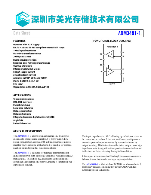
Data SheetADM3491-1FEATURESOperates with 3.3 V supplyEIA RS-422 and RS-485 compliant over full CM range 19 kΩ input impedanceUp to 50 transceivers on bus 20 Mbps data rateShort-circuit protectionSpecified over full temperature range Thermal shutdownInteroperable with 5 V logic 840 μA supply current 2 nA shutdown currentAvailable in PDIP , SOIC, and TSSOP Meets IEC1000-4-4 (>1 kV) 8 ns skewUpgrade for MAX3491, SN75ALS180APPLICATIONSTelecommunications DTE–DCE interface Packet switching Local area networks Data concentration Data multiplexersIntegrated services digital network (ISDN) AppleTalkIndustrial controlsGENERAL DESCRIPTIONThe ADM3491-1 is a low power, differential line transceiver designed to operate using a single 3.3 V power supply. Low power consumption, coupled with a shutdown mode, makes it ideal for power-sensitive applications. It is suitable for commu-nication on multipoint bus transmission lines.The ADM3491-1 is intended for balanced data transmission and complies with both Electronic Industries Association (EIA) Standards RS-485 and RS-422. It contains a differential line driver and a differential line receiver, making it suitable for full-duplex data transfer.FUNCTIONAL BLOCK DIAGRAMABZY05234-001The input impedance is 19 kΩ, allowing up to 50 transceivers to be connected on the bus. A thermal shutdown circuit prevents excessive power dissipation caused by bus contention or byoutput shorting. This feature forces the driver output into a high impedance state if a significant temperature increase is detected in the internal driver circuitry during fault conditions. If the inputs are unconnected (floating), the receiver contains a fail-safe feature that results in a logic high output state. The ADM3491-1 is fabricated on BiCMOS, an advanced mixed technology process combining low power CMOS with fast switching bipolar technology.TIMING SPECIFICATIONSV CC = 3.3 V, T A = 25°C, unless otherwise noted.Table 2.Parameter Min Typ Max Unit Test Conditions/ CommentsDRIVERDifferential Output Delay, T DD 1 35 ns R L = 60 Ω, C L1 = C L2 = 15 pF, see Figure 18 Differential Output Transition Time 1 8 15 ns R L = 60 Ω, C L1 = C L2 = 15 pF, see Figure 18 Propagation Delay Input to Output, T PLH, T PHL7 22 35 ns R L = 27 Ω, C L1 = C L2 = 15 pF, see Figure 19Driver Output to Output, T SKEW8 ns R L = 54 Ω, C L1 = C L2 = 15 pF, see Figure 19ENABLE/DISABLEDriver Enable to Output Valid 45 90 ns R L = 110 Ω, C L = 50 pF, see Figure 16Driver Disable Timing 40 80 ns R L = 110 Ω, C L = 50 pF, see Figure 16Driver Enable from Shutdown 65 110 ns R L = 110 Ω, C L = 15 pF, see Figure 16RECEIVERTime to Shutdown 80 190 300 nsPropagation Delay Input to Output, T PLH, T PHL25 65 90 ns C L = 15 pF, see Figure 21Skew, T PLH – T PHL10 ns C L = 15 pF, see Figure 21ns C L = 15 pF, see Figure 17Receiver Enable, T EN25 50Receiver Disable, T DEN25 45 ns C L = 15 pF, see Figure 17Receiver Enable from Shutdown 500 ns C L = 15 pF, see Figure 17V CC = 3.3 V ± 0.3 V, T A = T MIN to T MAX, unless otherwise noted.Table 3.Parameter MinConditions/CommentsUnitTestTypMaxDRIVERDifferential Output Delay, T DD 1 70 ns R L = 60 Ω, C L1 = C L2 = 15 pF, see Figure 18 Differential Output Transition Time 2 8 15 ns R L = 60 Ω, C L1 = C L2 = 15 pF, see Figure 18 Propagation Delay Input to Output, T PLH, T PHL7 22 70 ns R L = 27 Ω, C L1 = C L2 = 15 pF, see Figure 19Driver Output to Output, T SKEW10 ns R L = 54 Ω, C L1 = C L2 = 15 pF, see Figure 19ENABLE/DISABLEDriver Enable to Output Valid 45 110 ns R L = 110 Ω, C L = 50 pF, see Figure 16Driver Disable Timing 40 110 ns R L = 110 Ω, C L = 50 pF, see Figure 16Driver Enable from Shutdown 65 110 ns R L = 110 Ω, C L = 15 pF, see Figure 16RECEIVERTime to Shutdown 50 190 500 nsPropagation Delay Input to Output, T PLH, T PHL25 65 115 ns C L = 15 pF, see Figure 21Skew, T PLH – T PHL20 ns C L = 15 pF, see Figure 21Receiver Enable, T EN25 50 ns C L = 15 pF, see Figure 17Receiver Disable, T DEN25 50 ns C L = 15 pF, see Figure 17Receiver Enable from Shutdown 600 ns C L = 15 pF, see Figure 17PIN CONFIGURATIONS AND FUNCTION DESCRIPTIONSV CC V CC AB Z YNCNC = NO CONNECT05234-002Figure 2. 14-Lead PDIP and 14-Lead SOIC Pin ConfigurationNC = NO CONNECTNCRO RE NC DI DE V CC A B NC NCGNDNCY Z NC 05234-003Figure 3. 16-Lead TSSOP Pin ConfigurationTEST CIRCUITS05234-004Figure 14. Driver Voltage Measurement Test Circuit05234-006Figure 18. Driver Differential Output Delay Test CircuitTHEORY OF OPERATIONDIFFERENTIAL DATA TRANSMISSIONDifferential data transmission is used to reliably transmit data at high rates over long distances and through noisy environments. Differential transmission nullifies the effects of ground shifts and noise signals that appear as common-mode voltages on the line. The two main standards approved by the EIA specify the electrical characteristics of transceivers used in differential data transmission:∙RS-422 standard specifies data rates up to 10 MBaud and line lengths up to 4000 ft. A single driver can drive atransmission line with up to 10 receivers.∙RS-485 standard was defined to cater to true multipoint communications. This standard meets or exceeds all therequirements of RS-422, but also allows multiple driversand receivers to be connected to a single bus. An extended common-mode range of −7 V to +12 V is defined.The most significant differentiator of the RS-485 standard is that the drivers can be disabled, thereby allowing more than one to be connected to a single line. Only one driver should be enabled at a time, but the RS-485 standard contains additional specifications to guarantee device safety in the event of line contention.Table 6. Comparison of RS-422 and RS-485 Interface Standards Specification RS-422 RS-485 Transmission Type Differential Differential Maximum Cable Length 4000 ft. 4000 ft. Minimum Driver Output Voltage ±2 V ±1.5 V Driver Load Impedance 100 Ω 54 Ω Receiver Input Resistance 4 kΩ min 12 kΩ min Receiver Input Sensitivity ±200 mV ±200 mV Receiver Input Voltage Range −7 V to +7 V −7 V to +12 VCABLE AND DATA RATEThe transmission line of choice for RS-485 communications is a twisted pair. Twisted pair cable tends to cancel common-mode noise and also causes cancellation of the magnetic fields gener-ated by the current flowing through each wire, thereby reducing the effective inductance of the pair.The ADM3491-1 is designed for bidirectional data communica-tions on multipoint transmission lines. A typical application showing a multipoint transmission network is illustrated in Figure 26. Only one driver can transmit at a particular time, but multiple receivers can be enabled simultaneously. As with any transmission line, it is important that reflections be minimized. This can be achieved by terminating the extreme ends of the line using resistors equal to the characteristic impedance of the line. Stub lengths of the main line should also be kept as short as possible. A properly terminated transmission line appears purely resistive to the driver. RECEIVER OPEN-CIRCUIT FAIL-SAFE FEATUREThe receiver input includes a fail-safe feature that guarantees a logic high on the receiver when the inputs are open circuit or floating.5234-26 Figure 26. ADM3491-1 Full-Duplex Data Link。

SRT versus ASRIf the normal T C limit of 85°C is not exceeded, then neither SRT nor ASR is required, andboth can be disabled throughout operation. However, if the extended temperature op-tion of 95°C is needed, the user is required to provide a 2x refresh rate during manualrefresh and to enable either the SRT or the ASR to ensure self refresh is performed at the2x rate.SRT forces the DRAM to switch the internal self refresh rate from 1x to 2x. Self refresh isperformed at the 2x refresh rate regardless of the case temperature.ASR automatically switches the DRAM’s internal self refresh rate from 1x to 2x. Howev-er, while in self refresh mode, ASR enables the refresh rate to automatically adjust be-tween 1x and 2x over the supported temperature range. One other disadvantage of ASRis the DRAM cannot always switch from a 1x to 2x refresh rate at an exact T C of 85°C.Although the DRAM will support data integrity when it switches from a 1x to 2x refreshrate, it may switch at a temperature lower than 85°C.Since only one mode is necessary, SRT and ASR cannot be enabled at the same time. Dynamic On-Die Termination (ODT)The dynamic ODT (R TT(WR)) feature is defined by MR2[10, 9]. Dynamic ODT is enabledwhen a value is selected for the dynamic ODT resistance R TT(WR). This new DDR3SDRAM feature enables the ODT termination resistance value to change without issu-ing an MRS command, essentially changing the ODT termination on-the-fly.With dynamic ODT (R TT(WR)) enabled, the DRAM switches from nominal ODT (R TT,nom)to dynamic ODT (R TT(WR)) when beginning a WRITE burst, and subsequently switchesback to normal ODT (R TT,nom) at the completion of the WRITE burst. If R TT,nom is disa-bled, the R TT,nom value will be High-Z. Special timing parameters must be adhered towhen dynamic ODT (R TT(WR)) is enabled: ODTLcnw, ODTLcwn4, ODTLcwn8, ODTH4,ODTH8, and t ADC.Dynamic ODT is only applicable during WRITE cycles. If normal ODT (R TT,nom) is disa-bled, dynamic ODT (R TT(WR)) is still permitted. R TT,nom and R TT(WR) can be used inde-pendent of one another. Dynamic ODT is not available during write leveling mode, re-gardless of the state of ODT (R TT,nom). For details on dynamic ODT operation, refer tothe Dynamic ODT section of the data sheet.Commands – Truth TablesTable 87: Truth Table – CommandNotes: mands are defined by the states of CS#, RAS#, CAS#, WE#, and CKE at the risingedge of the clock. The MSB of BA, RA, and CA are device-, density-, and configuration-dependent.。

Low-Power, Slew-Rate-Limited RS-485/RS-422 Transceivers12MAX481/MAX483/MAX485/MAX487–MAX491/MAX1487500mV/div 20ns/div ABRO 2V/divV CC = 5V T A = +25°C 500mV/div 20ns/divAB RO2V/divV CC = 5V T A = +25°C500mV/div 400ns/div ABRO2V/div V CC = 5V T A = +25°C 500mV/div 400ns/divA B RO2V/div V CC = 5VT A = +25°CFigure 14. Receiver Propagation Delay Test CircuitFigure 15. MAX481/MAX485/MAX490/MAX491/MAX1487Receiver t PHL Figure 16. MAX481/MAX485/MAX490/MAX491/MAX1487Receiver t PLHPHL Figure 18. MAX483, MAX487–MAX489 Receiver t PLHLow-Power, Slew-Rate-Limited RS-485/RS-422 Transceivers 8MAX481/MAX483/MAX485/MAX487–MAX491/MAX1487__________Applications Information The MAX481/MAX483/MAX485/MAX487–MAX491 and MAX1487 are low-power transceivers for RS-485 and RS-422 communications. The MAX481, MAX485, MAX490,MAX491, and MAX1487 can transmit and receive at data rates up to 2.5Mbps, while the MAX483, MAX487,MAX488, and MAX489 are specified for data rates up to 250kbps. The MAX488–MAX491 are full-duplex trans-ceivers while the MAX481, MAX483, MAX485, MAX487,and MAX1487 are half-duplex. In addition, Driver Enable (DE) and Receiver Enable (RE ) pins are included on the MAX481, MAX483, MAX485, MAX487, MAX489,MAX491, and MAX1487. When disabled, the driver and receiver outputs are high impedance.MAX487/MAX1487:128 Transceivers on the Bus The 48k Ω, 1/4-unit-load receiver input impedance of the MAX487 and MAX1487 allows up to 128 transceivers on a bus, compared to the 1-unit load (12k Ωinput impedance) of standard RS-485 drivers (32 trans-ceivers maximum). Any combination of MAX487/MAX1487 and other RS-485 transceivers with a total of 32 unit loads or less can be put on the bus. The MAX481/MAX483/MAX485 and MAX488–MAX491 have standard 12k ΩReceiver Input impedance.Figure 2. MAX488/MAX490 Pin Configuration and Typical Operating Circuit Figure 3. MAX489/MAX491 Pin Configuration and Typical Operating Circuit。

Dynamic ODTIn certain application cases and to further enhance signal integrity on the data bus, it isdesirable that the termination strength of the device can be changed without issuing anMRS command. This requirement is supported by the dynamic ODT feature.Functional DescriptionDynamic ODT mode is enabled if bit A9 or A10 of MR2 is set to 1.•Three R TT values are available: R TT(NOM), R TT(WR), and R TT(Park).–The value for R TT(NOM) is preselected via bits MR1[10:8].–The value for R TT(WR) is preselected via bits MR2[11:9].–The value for R TT(Park) is preselected via bits MR5[8:6].•During operation without WRITE commands, the termination is controlled as fol-lows:–Nominal termination strength R TT(NOM) or R TT(Park) is selected.–R TT(NOM) on/off timing is controlled via ODT pin and latencies DODTLon andDODTLoff, and R TT(Park) is on when ODT is LOW.•When a WRITE command (WR, WRA, WRS4, WRS8, WRAS4, and WRAS8) is regis-tered, and if dynamic ODT is enabled, the termination is controlled as follows:–Latency ODTLcnw after the WRITE command, termination strength R TT(WR) is se-lected.–Latency ODTLcwn8 (for BL8, fixed by MRS or selected OTF) or ODTLcwn4 (forBC4, fixed by MRS or selected OTF) after the WRITE command, terminationstrength R TT(WR) is de-selected.One or two clocks will be added into or subtracted from ODTLcwn8 and ODTLcwn4,depending on write CRC mode and/or 2t CK preamble enablement.The following table shows latencies and timing parameters relevant to the on-die termi-nation control in dynamic ODT mode. The dynamic ODT feature is not supported inDLL-off mode. An MRS command must be used to set R TT(WR) to disable dynamic ODTexternally (MR2[11:9] = 000).Table 74: Dynamic ODT Latencies and Timing (1t CK Preamble Mode and CRC Disabled)4Gb: x4, x8, x16 DDR4 SDRAM Dynamic ODTFigure 161: READ (BC4: Fixed) to WRITE (BC4: Fixed) with 1t CK Preamble and Write CRC in Same or Different Bank GroupCommand DQ x4,BC = 4 (Fixed)CK_t CK_cDQS_t,DQS_cBank GroupAddress AddressDQ x8/X16,BC = 4 (Fixed)Notes: 1.BC = 4 (Fixed), RL = 11 (CL = 11, AL = 0), READ preamble = 1t CK, WL = 9 (CWL = 9, AL =0), WRITE preamble = 1t CK.2.DO n = data-out from column n , DI b = data-in from column b .3.DES commands are shown for ease of illustration; other commands may be valid atthese times.4.BC4 setting activated by MR0[1:0] = 10.5.CA parity = Disable, CS to CA latency = Disable, Read DBI = Disable, Write DBI = Disable,Write CRC = Enable.READ Operation with Command/Address Latency (CAL) EnabledFigure 162: Consecutive READ (BL8) with CAL (3t CK) and 1t CK Preamble in Different Bank GroupCommandw/o CS_nDQCK_tCK_cDQS_t,DQS_cBank GroupAddress Address CS_n Notes: 1.BL = 8, RL = 11 (CL = 11, AL = 0), READ preamble = 1t CK.4Gb: x4, x8, x16 DDR4 SDRAM READ Operation。

ADM485FUNCTIONAL BLOCK DIAGRAMCC 00078-001FEATURESMeets EIA RS-485 standard 5 Mbps data rateSingle 5 V supply–7 V to +12 V bus common-mode range High speed, low power BiCMOS Thermal shutdown protection Short-circuit protectionDriver propagation delay: 10 ns typical Receiver propagation delay: 15 ns typical High-Z outputs with power off Superior upgrade for LTC485APPLICATIONSLow power RS-485 systems DTE/DCE interface Packet switchingLocal area networks (LNAs) Data concentration Data multiplexersIntegrated services digital network (ISDN)GENERAL DESCRIPTIONThe ADM485 is a differential line transceiver suitable for high speed bidirectional data communication on multipoint bus transmission lines. It is designed for balanced data transmission and complies with EIA standards RS-485 and RS-422. The part contains a differential line driver and a differential line receiver. Both the driver and the receiver can be enabled independently. When disabled, the outputs are three-stated.The ADM485 operates from a single 5 V power supply. Excessive power dissipation caused by bus contention or by output shorting is prevented by a thermal shutdown circuit. If during fault conditions, a significant temperature increase is detected in the internal driver circuitry, this feature forces the driver output into a high impedance state.Up to 32 transceivers can be connected simultaneously on a bus, but only one driver should be enabled at any time. It is important, therefore, that the remaining disabled drivers do not load the bus. To ensure this, the ADM485 driver features high output impedance when disabled and when powered down, which minimizes the loading effect when the transceiver is not being used. The high impedance driver output is maintained over the common-mode voltage range of −7 V to +12 V .Figure 1.The receiver contains a fail-safe feature that results in a logic high output state if the inputs are unconnected (floating). The ADM485 is fabricated on BiCMOS, an advanced mixed technology process combining low power CMOS with fast switching bipolar technology. All inputs and outputs contain protection against ESD; all driver outputs feature high source and sink current capability. An epitaxial layer is used to guard against latch-up.The ADM485 features extremely fast switching speeds. Minimal driver propagation delays permit transmission at data rates up to 5 Mbps while low skew minimizes EMI interference. The part is fully specified over the commercial and industrial temperature range and is available in 8-lead PDIP , 8-lead SOIC, and small footprint, 8-lead MSOP packages.ADM485Rev. F | Page 2 of 16ADM485SPECIFICATIONSV CC = 5 V ± 5%, all specifications T MIN to T MAX, unless otherwise noted.Rev. F | Page 3 of 16ADM485TIMING SPECIFICATIONSV CC = 5 V ± 5%, all specifications T MIN to T MAX, unless otherwise noted.1 Guaranteed by characterization.Rev. F | Page 4 of 16ADM485Rev. F | Page 5 of 16ABSOLUTE MAXIMUM RATINGST A = 25°C, unless otherwise noted.Stresses above those listed under Absolute Maximum Ratings may cause permanent damage to the device. This is a stress rating only; functional operation of the device at these or any other conditions above those indicated in the operationalsection of this specification is not implied. Exposure to absolute maximum rating conditions for extended periods may affect device reliability.Table 4. TransmittingInputsOutputsDE DIB A 1 1 0 1 1 0 1 0 0X 1Z 2Z 21 X = don’t care.2Z = high impedance.1 X = don’t care.2Z = high impedance.ESD CAUTION。
General Description The MAX481E, MAX483E, MAX485E, MAX487E–MAX491E, and MAX1487E are low-power transceivers for RS-485 and RS-422 communications in harsh environ-ments. Each driver output and receiver input is protected against ±15kV electro-static discharge (ESD) shocks, without latchup. These parts contain one driver and one receiver. The MAX483E, MAX487E, MAX488E, and MAX489E feature reduced slew-rate drivers that minimize EMI and reduce reflections caused by improperly termi-nated cables, thus allowing error-free data transmission up to 250kbps. The driver slew rates of the MAX481E, MAX485E, MAX490E, MAX491E, and MAX1487E are not limited, allowing them to transmit up to 2.5Mbps.These transceivers draw as little as 120µA supply cur-rent when unloaded or when fully loaded with disabled drivers (see Selector Guide). Additionally, the MAX481E, MAX483E, and MAX487E have a low-current shutdown mode in which they consume only 0.5µA. All parts oper-ate from a single +5V supply.Drivers are short-circuit current limited, and are protected against excessive power dissipation by thermal shutdown circuitry that places their outputs into a high-impedance state. The receiver input has a fail-safe feature that guar-antees a logic-high output if the input is open circuit.The MAX487E and MAX1487E feature quarter-unit-load receiver input impedance, allowing up to 128 trans-ceivers on the bus. The MAX488E–MAX491E are designed for full-duplex communications, while the MAX481E, MAX483E, MAX485E, MAX487E, and MAX1487E are designed for half-duplex applications. For applications that are not ESD sensitive see the pin-and function-compatible MAX481, MAX483, MAX485, MAX487–MAX491, and MAX1487.Applications Low-Power RS-485 TransceiversLow-Power RS-422 TransceiversLevel TranslatorsTransceivers for EMI-Sensitive ApplicationsIndustrial-Control Local Area NetworksNext-Generation Device Features ♦For Fault-Tolerant Applications:MAX3430: ±80V Fault-Protected, Fail-Safe, 1/4-Unit Load, +3.3V, RS-485 TransceiverMAX3080–MAX3089: Fail-Safe, High-Speed(10Mbps), Slew-Rate-Limited, RS-485/RS-422Transceivers♦For Space-Constrained Applications:MAX3460–MAX3464: +5V, Fail-Safe, 20Mbps,Profibus, RS-485/RS-422 TransceiversMAX3362: +3.3V, High-Speed, RS-485/RS-422Transceiver in a SOT23 PackageMAX3280E–MAX3284E: ±15kV ESD-Protected,52Mbps, +3V to +5.5V, SOT23, RS-485/RS-422True Fail-Safe ReceiversMAX3030E–MAX3033E: ±15kV ESD-Protected,+3.3V, Quad RS-422 Transmitters♦For Multiple Transceiver Applications:MAX3293/MAX3294/MAX3295: 20Mbps, +3.3V,SOT23, RS-485/RS-422 Transmitters♦For Fail-Safe Applications:MAX3440E–MAX3444E: ±15kV ESD-Protected,±60V Fault-Protected, 10Mbps, Fail-SafeRS-485/J1708 Transceivers♦For Low-Voltage Applications:MAX3483E/MAX3485E/MAX3486E/MAX3488E/MAX3490E/MAX3491E: +3.3V Powered, ±15kVESD-Protected, 12Mbps, Slew-Rate-Limited,True RS-485/RS-422 Transceivers±15kV ESD-Protected, Slew-Rate-Limited, Low-Power, RS-485/RS-422 TransceiversOrdering InformationOrdering Information continued at end of data sheet.Selector Guide appears at end of data sheet.±15kV ESD-Protected, Slew-Rate-Limited,Low-Power, RS-485/RS-422 Transceivers__________Function Tables (MAX481E/MAX483E/MAX485E/MAX487E/MAX1487E)Table 1. TransmittingTable 2. Receivingneers developed state-of-the-art structures to protect these pins against ESD of ±15kV without damage. The ESD structures withstand high ESD in all states: normal operation, shutdown, and powered down. After an ESD event, Maxim’s MAX481E, MAX483E, MAX485E, MAX487E–MAX491E, and MAX1487E keep working without latchup.ESD protection can be tested in various ways; the transmitter outputs and receiver inputs of this product family are characterized for protection to ±15kV using the Human Body Model.Other ESD test methodologies include IEC10004-2 con-tact discharge and IEC1000-4-2 air-gap discharge (for-merly IEC801-2).ESD Test ConditionsESD performance depends on a variety of conditions.Contact Maxim for a reliability report that documents test set-up, test methodology, and test results.Human Body ModelF igure 4 shows the Human Body Model, and F igure 5shows the current waveform it generates when dis-charged into a low impedance. This model consists of a 100pF capacitor charged to the ESD voltage of inter-est, which is then discharged into the test device through a 1.5k Ωresistor.IEC1000-4-2The IEC1000-4-2 standard covers ESD testing and per-formance of finished equipment; it does not specifically refer to integrated circuits (Figure 6).MAX481E/MAX483E/MAX485E/ MAX487E–MAX491E/MAX1487E__________Applications InformationThe MAX481E/MAX483E/MAX485E/MAX487E–MAX491E and MAX1487E are low-power transceivers for RS-485 and RS-422 communications. These “E” versions of the MAX481, MAX483, MAX485, MAX487–MAX491, and MAX1487 provide extra protection against ESD. The rugged MAX481E, MAX483E, MAX485E, MAX497E–MAX491E, and MAX1487E are intended for harsh envi-ronments where high-speed communication is important. These devices eliminate the need for transient suppres-sor diodes and the associated high capacitance loading.The standard (non-“E”) MAX481, MAX483, MAX485, MAX487–MAX491, and MAX1487 are recommended for applications where cost is critical.The MAX481E, MAX485E, MAX490E, MAX491E, and MAX1487E can transmit and receive at data rates up to 2.5Mbps, while the MAX483E, MAX487E, MAX488E, and MAX489E are specified for data rates up to 250kbps. The MAX488E–MAX491E are full-duplex transceivers, while the MAX481E, MAX483E, MAX487E, and MAX1487E are half-duplex. In addition, driver-enable (DE) and receiver-enable (RE) pins are included on the MAX481E, MAX483E, MAX485E, MAX487E, MAX489E, MAX491E, and MAX1487E. When disabled, the driver and receiver outputs are high impedance.±15kV ESD ProtectionAs with all Maxim devices, ESD-protection structures are incorporated on all pins to protect against electro-static discharges encountered during handling and assembly. The driver outputs and receiver inputs have extra protection against static electricity. Maxim’s engi-±15kV ESD-Protected, Slew-Rate-Limited,Low-Power, RS-485/RS-422 TransceiversFigure 6. IEC1000-4-2 ESD Test ModelFigure 8. Driver DC Test LoadFigure 7. IEC1000-4-2 ESD Generator Current WaveformFigure 9. Receiver Timing Test LoadFigure 4. Human Body ESD Test ModelFigure 5. Human Body Model Current WaveformMAX481E/MAX483E/MAX485E/ MAX487E–MAX491E/MAX1487E±15kV ESD-Protected, Slew-Rate-Limited,Low-Power, RS-485/RS-422 Transceiversdelay times. Typical propagation delays are shown in Figures 19–22 using Figure 18’s test circuit.The difference in receiver delay times, t PLH - t PHL , is typically under 13ns for the MAX481E, MAX485E,MAX490E, MAX491E, and MAX1487E, and is typically less than 100ns for the MAX483E and MAX487E–MAX489E.The driver skew times are typically 5ns (10ns max) for the MAX481E, MAX485E, MAX490E, MAX491E, and MAX1487E, and are typically 100ns (800ns max) for the MAX483E and MAX487E–MAX489E.Typical ApplicationsThe MAX481E, MAX483E, MAX485E, MAX487E–MAX491E, and MAX1487E transceivers are designed for bidirectional data communications on multipoint bus transmission lines. F igures 25 and 26 show typical net-work application circuits. These parts can also be used as line repeaters, with cable lengths longer than 4000 feet.To minimize reflections, the line should be terminated at both ends in its characteristic impedance, and stub lengths off the main line should be kept as short as possi-ble. The slew-rate-limited MAX483E and MAX487E–MAX489E are more tolerant of imperfect termination.Bypass the V CC pin with 0.1µF.Isolated RS-485For isolated RS-485 applications, see the MAX253 and MAX1480 data sheets.Line Length vs. Data RateThe RS-485/RS-422 standard covers line lengths up to 4000 feet. Figures 23 and 24 show the system differen-tial voltage for the parts driving 4000 feet of 26AWG twisted-pair wire at 110kHz into 100Ωloads.Figure 18. Receiver Propagation Delay Test CircuitIt takes the drivers and receivers longer to become enabled from the low-power shutdown state (t ZH(SHDN ), t ZL(SHDN)) than from the operating mode (t ZH , t ZL ). (The parts are in operating mode if the RE, DE inputs equal a logical 0,1 or 1,1 or 0, 0.)Driver Output ProtectionExcessive output current and power dissipation caused by faults or by bus contention are prevented by two mechanisms. A foldback current limit on the output stage provides immediate protection against short circuits over the whole common-mode voltage range (see Typical Operating Characteristics ). In addition, a thermal shut-down circuit forces the driver outputs into a high-imped-ance state if the die temperature rises excessively.Propagation DelayMany digital encoding schemes depend on the differ-。
Figure 59: Consecutive WRITE-to-WRITECKCK#CommandAddressDQDQS, DQS#DMDon’t Care Transitioning Data t DQSS (NOM)Notes: 1.Subsequent rising DQS signals must align to the clock within t DQSS.2.DI b , etc. = data-in for column b , etc.3.Three subsequent elements of data-in are applied in the programmed order following DI b .4.Three subsequent elements of data-in are applied in the programmed order following DI n .5.Shown with BL = 4, AL = 0, CL = 3; thus, WL = 2.6.Each WRITE command may be to any bank.Figure 60: Nonconsecutive WRITE-to-WRITECKCK#CommandAddressT0T1T2T3T2n T4T5T4n T3n T5n T6T6nDQDQS, DQS#DM t Don’t CareTransitioning Data Notes: 1.Subsequent rising DQS signals must align to the clock within t DQSS.2.DI b (or n ), etc. = data-in for column b (or column n ).3.Three subsequent elements of data-in are applied in the programmed order following DI b .4.Three subsequent elements of data-in are applied in the programmed order following DI n .5.Shown with BL = 4, AL = 0, CL = 3; thus, WL = 2.6.Each WRITE command may be to any bank.2Gb: x4, x8, x16 DDR2 SDRAM WRITETable 28: AC Input Test Conditions (Continued)Notes: 1.All voltages referenced to V SS .2.Input waveform setup timing (t IS b ) is referenced from the input signal crossing at the V IH(AC) level for a rising signal and V IL(AC) for a falling signal applied to the device under test, as shown in Figure 32 (page 70).3.See Input Slew Rate Derating (page 59).4.The slew rate for single-ended inputs is measured from DC level to AC level, V IL(DC) to V IH(AC) on the rising edge and V IL(AC) to V IH(DC) on the falling edge. For signals referenced to V REF , the valid intersection is where the “tangent” line intersects V REF , as shown in Figure 25 (page 62), Figure 27 (page 63), Figure 29 (page 68), and Figure 31(page 69).5.Input waveform hold (t IH b ) timing is referenced from the input signal crossing at the V IL(DC) level for a rising signal and V IH(DC) for a falling signal applied to the device under test, as shown in Figure 32 (page 70).6.Input waveform setup timing (t DS) and hold timing (t DH) for single-ended data strobe is referenced from the crossing of DQS, UDQS, or LDQS through the Vref level applied to the device under test, as shown in Figure 34 (page 71).7.Input waveform setup timing (t DS) and hold timing (t DH) when differential data strobe is enabled is referenced from the cross-point of DQS/DQS#, UDQS/UDQS#, or LDQS/LDQS#, as shown in Figure 33 (page 70).8.Input waveform timing is referenced to the crossing point level (V IX ) of two input signals (V TR and V CP ) applied to the device under test, where V TR is the true input signal and V CP is the complementary input signal, as shown in Figure 35 (page 71).9.The slew rate for differentially ended inputs is measured from twice the DC level to twice the AC level: 2 × V IL(DC) to 2 × V IH(AC) on the rising edge and 2 × V IL(AC) to 2 ×V IH(DC) on the falling edge. For example, the CK/CK# would be –250mV to 500mV for CK rising edge and would be 250mV to –500mV for CK falling edge.2Gb: x4, x8, x16 DDR2 SDRAM AC Overshoot/Undershoot SpecificationFigure 5: Functional Block Diagram – 128 Meg x 162Gb: x4, x8, x16 DDR2 SDRAM Functional Block Diagrams。
PRECHARGEThe PRECHARGE command is used to deactivate the open row in a particular bank orthe open row in all banks. The bank(s) will be available for a subsequent row activationa specified time (t RP) after the PRECHARGE command is issued, except in the case ofconcurrent auto precharge, where a READ or WRITE command to a different bank is al-lowed as long as it does not interrupt the data transfer in the current bank and does notviolate any other timing parameters. After a bank has been precharged, it is in the idlestate and must be activated prior to any READ or WRITE commands being issued tothat bank. A PRECHARGE command is allowed if there is no open row in that bank (idlestate) or if the previously open row is already in the process of precharging. However,the precharge period will be determined by the last PRECHARGE command issued tothe bank.REFRESHREFRESH is used during normal operation of the DDR2 SDRAM and is analogous toCAS#-before-RAS# (CBR) REFRESH. All banks must be in the idle mode prior to issuinga REFRESH command. This command is nonpersistent, so it must be issued each timea refresh is required. The addressing is generated by the internal refresh controller. Thismakes the address bits a “Don’t Care” during a REFRESH command.SELF REFRESHThe SELF REFRESH command can be used to retain data in the DDR2 SDRAM, even ifthe rest of the system is powered down. When in the self refresh mode, the DDR2SDRAM retains data without external clocking. All power supply inputs (including Vref)must be maintained at valid levels upon entry/exit and during SELF REFRESH opera-tion.The SELF REFRESH command is initiated like a REFRESH command except CKE isLOW. The DLL is automatically disabled upon entering self refresh and is automaticallyenabled upon exiting self refresh.Mode Register (MR)The mode register is used to define the specific mode of operation of the DDR2 SDRAM.This definition includes the selection of a burst length, burst type, CAS latency, operat-ing mode, DLL RESET, write recovery, and power-down mode, as shown in Figure 36(page 79). Contents of the mode register can be altered by re-executing the LOADMODE (LM) command. If the user chooses to modify only a subset of the MR variables,all variables must be programmed when the command is issued.The MR is programmed via the LM command and will retain the stored information un-til it is programmed again or until the device loses power (except for bit M8, which isself-clearing). Reprogramming the mode register will not alter the contents of the mem-ory array, provided it is performed correctly.The LM command can only be issued (or reissued) when all banks are in the prechargedstate (idle state) and no bursts are in progress. The controller must wait the specifiedtime t MRD before initiating any subsequent operations such as an ACTIVATE com-mand. Violating either of these requirements will result in an unspecified operation.READ with auto precharge enabled/ WRITE with auto precharge enabled:The READ with auto precharge enabled or WRITE with auto pre-charge enabled states can each be broken into two parts: the ac-cess period and the precharge period. For READ with auto pre-charge, the precharge period is defined as if the same burst was executed with auto precharge disabled and then followed with the earliest possible PRECHARGE command that still accesses all of the data in the burst. For WRITE with auto precharge, the pre-charge period begins when t WR ends, with t WR measured as if auto precharge was disabled. The access period starts with regis-tration of the command and ends where the precharge period (or t RP) begins. This device supports concurrent auto precharge such that when a READ with auto precharge is enabled or a WRITE with auto precharge is enabled, any command to other banks is allowed, as long as that command does not interrupt the read or write data transfer already in process. In either case, all other related limitations apply (contention between read da-ta and write data must be avoided).The minimum delay from a READ or WRITE command with auto precharge enabled toa command to a different bank is summarized in Table 40 (page 76).4.REFRESH and LOAD MODE commands may only be issued when all banks are idle.5.Not used.6.All states and sequences not shown are illegal or reserved.7.READs or WRITEs listed in the Command/Action column include READs or WRITEs withauto precharge enabled and READs or WRITEs with auto precharge disabled.8. A WRITE command may be applied after the completion of the READ burst.9.Requires appropriate DM.10.The number of clock cycles required to meet t WTR is either two or t WTR/t CK, whicheveris greater.Table 40: Minimum Delay with Auto Precharge EnabledDESELECTThe DESELECT function (CS# HIGH) prevents new commands from being executed bythe DDR2 SDRAM. The DDR2 SDRAM is effectively deselected. Operations already inprogress are not affected. DESELECT is also referred to as COMMAND INHIBIT.。
Asynchronous ODT ModeAsynchronous ODT mode is selected when the DRAM runs in DLL-off mode. In asyn-chronous ODT timing mode, the internal ODT command is not delayed by either addi-tive latency (AL) or the parity latency (PL) relative to the external ODT signal (R TT(NOM)).In asynchronous ODT mode, two timing parameters apply: t AONAS (MIN/MAX), and t AOFAS (MIN/MAX).R TT(NOM) Turn-on Time•Minimum R TT(NOM) turn-on time (t AONAS [MIN]) is when the device termination cir-cuit leaves R TT(Park) and ODT resistance begins to turn on.•Maximum R TT(NOM) turn-on time (t AONAS [MAX]) is when the ODT resistance has reached R TT(NOM).•t AONAS (MIN) and t AONAS (MAX) are measured from ODT being sampled HIGH.R TT(NOM) Turn-off Time•Minimum R TT(NOM) turn-off time (t AOFAS [MIN]) is when the device's termination circuit starts to leave R TT(NOM).•Maximum R TT(NOM) turn-off time (t AOFAS [MAX]) is when the on-die termination has reached R TT(Park).•t AOFAS (MIN) and t AOFAS (MAX) are measured from ODT being sampled LOW.Figure 208: Asynchronous ODT Timings with DLL Offdiff_CKCKEODTR TT T1T0T2T3T4T5T6Ti Ti + 1Ti + 2Ti + 3Ti + 4Ti + 5Ti + 6Ta TbTransitioningWRITE OperationWrite Timing DefinitionsThe write timings shown in the following figures are applicable in normal operation mode, that is, when the DLL is enabled and locked.Write Timing – Clock-to-Data Strobe RelationshipThe clock-to-data strobe relationship is shown below and is applicable in normal oper-ation mode, that is, when the DLL is enabled and locked.Rising data strobe edge parameters:•t DQSS (MIN) to t DQSS (MAX) describes the allowed range for a rising data strobe edge relative to CK.•t DQSS is the actual position of a rising strobe edge relative to CK.•t DQSH describes the data strobe high pulse width.•t WPST strobe going to HIGH, nondrive level (shown in the postamble section of the graphic below).Falling data strobe edge parameters:•t DQSL describes the data strobe low pulse width.•t WPRE strobe going to LOW, initial drive level (shown in the preamble section of the graphic below).4Gb: x4, x8, x16 DDR4 SDRAM WRITE Operation。